2. 1N4001, 1N4002, 1N4003, 1N4004, 1N4005, 1N4006, 1N4007
http://onsemi.com
2
MAXIMUM RATINGS
Rating Symbol 1N4001 1N4002 1N4003 1N4004 1N4005 1N4006 1N4007 Unit
†Peak Repetitive Reverse Voltage
Working Peak Reverse Voltage
DC Blocking Voltage
VRRM
VRWM
VR
50 100 200 400 600 800 1000 V
†Non−Repetitive Peak Reverse Voltage
(halfwave, single phase, 60 Hz)
VRSM 60 120 240 480 720 1000 1200 V
†RMS Reverse Voltage VR(RMS) 35 70 140 280 420 560 700 V
†Average Rectified Forward Current
(single phase, resistive load,
60 Hz, TA = 75°C)
IO 1.0 A
†Non−Repetitive Peak Surge Current
(surge applied at rated load conditions)
IFSM 30 (for 1 cycle) A
Operating and Storage Junction
Temperature Range
TJ
Tstg
−65 to +175 °C
Stresses exceeding Maximum Ratings may damage the device. Maximum Ratings are stress ratings only. Functional operation above the
Recommended Operating Conditions is not implied. Extended exposure to stresses above the Recommended Operating Conditions may affect
device reliability.
†Indicates JEDEC Registered Data
THERMAL CHARACTERISTICS
Rating Symbol Max Unit
Maximum Thermal Resistance, Junction−to−Ambient RqJA Note 1 °C/W
ELECTRICAL CHARACTERISTICS†
Rating Symbol Typ Max Unit
Maximum Instantaneous Forward Voltage Drop, (iF = 1.0 Amp, TJ = 25°C) vF 0.93 1.1 V
Maximum Full−Cycle Average Forward Voltage Drop, (IO = 1.0 Amp, TL = 75°C, 1 inch leads) VF(AV) − 0.8 V
Maximum Reverse Current (rated DC voltage)
(TJ = 25°C)
(TJ = 100°C)
IR
0.05
1.0
10
50
mA
Maximum Full−Cycle Average Reverse Current, (IO = 1.0 Amp, TL = 75°C, 1 inch leads) IR(AV) − 30 mA
†Indicates JEDEC Registered Data
4. 1N4001, 1N4002, 1N4003, 1N4004, 1N4005, 1N4006, 1N4007
http://onsemi.com
4
Lead Length, LMounting
Method 1/8 1/4 1/2 Units
1
2
3
52
67RqJA
65 72
80 87
50
°C/W
°C/W
°C/W
TYPICAL VALUES FOR RqJA IN STILL AIR
Data shown for thermal resistance, junction−to−ambient
(RqJA) for the mountings shown is to be used as typical
guideline values for preliminary engineering or in case the
tie point temperature cannot be measured.
NOTE 1. − AMBIENT MOUNTING DATA
MOUNTING METHOD 1
MOUNTING METHOD 2
MOUNTING METHOD 3
ÉÉÉÉÉÉÉÉÉÉÉ
ÉÉÉÉÉÉÉÉÉÉÉ
L L
ÉÉÉÉÉÉÉÉÉÉÉÉ
ÉÉÉÉÉÉÉÉÉÉÉÉ
L L
Vector Pin Mounting
ÉÉÉÉ
ÉÉ
ÉÉ
ÉÉ
ÉÉ
ÉÉ
L = 3/8
Board Ground Plane
P.C. Board with
1−1/2 X 1−1/2 Copper Surface″″
″
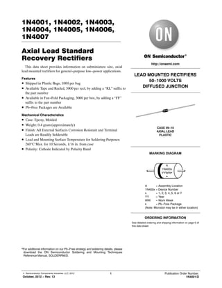
7. 1N4001, 1N4002, 1N4003, 1N4004, 1N4005, 1N4006, 1N4007
http://onsemi.com
7
PACKAGE DIMENSIONS
AXIAL LEAD
CASE 59−10
ISSUE U
B
DK
K
F
F
A
DIM MIN MAX MIN MAX
MILLIMETERSINCHES
A 4.10 5.200.161 0.205
B 2.00 2.700.079 0.106
D 0.71 0.860.028 0.034
F −−− 1.27−−− 0.050
K 25.40 −−−1.000 −−−
NOTES:
1. DIMENSIONING AND TOLERANCING PER ANSI
Y14.5M, 1982.
2. CONTROLLING DIMENSION: INCH.
3. ALL RULES AND NOTES ASSOCIATED WITH
JEDEC DO−41 OUTLINE SHALL APPLY
4. POLARITY DENOTED BY CATHODE BAND.
5. LEAD DIAMETER NOT CONTROLLED WITHIN F
DIMENSION.
POLARITY INDICATOR
OPTIONAL AS NEEDED
(SEE STYLES)
ON Semiconductor and are registered trademarks of Semiconductor Components Industries, LLC (SCILLC). SCILLC owns the rights to a number of patents, trademarks,
copyrights, trade secrets, and other intellectual property. A listing of SCILLC’s product/patent coverage may be accessed at www.onsemi.com/site/pdf/Patent−Marking.pdf. SCILLC
reserves the right to make changes without further notice to any products herein. SCILLC makes no warranty, representation or guarantee regarding the suitability of its products for any
particular purpose, nor does SCILLC assume any liability arising out of the application or use of any product or circuit, and specifically disclaims any and all liability, including without
limitation special, consequential or incidental damages. “Typical” parameters which may be provided in SCILLC data sheets and/or specifications can and do vary in different applications
and actual performance may vary over time. All operating parameters, including “Typicals” must be validated for each customer application by customer’s technical experts. SCILLC
does not convey any license under its patent rights nor the rights of others. SCILLC products are not designed, intended, or authorized for use as components in systems intended for
surgical implant into the body, or other applications intended to support or sustain life, or for any other application in which the failure of the SCILLC product could create a situation where
personal injury or death may occur. Should Buyer purchase or use SCILLC products for any such unintended or unauthorized application, Buyer shall indemnify and hold SCILLC and
its officers, employees, subsidiaries, affiliates, and distributors harmless against all claims, costs, damages, and expenses, and reasonable attorney fees arising out of, directly or indirectly,
any claim of personal injury or death associated with such unintended or unauthorized use, even if such claim alleges that SCILLC was negligent regarding the design or manufacture
of the part. SCILLC is an Equal Opportunity/Affirmative Action Employer. This literature is subject to all applicable copyright laws and is not for resale in any manner.
PUBLICATION ORDERING INFORMATION
N. American Technical Support: 800−282−9855 Toll Free
USA/Canada
Europe, Middle East and Africa Technical Support:
Phone: 421 33 790 2910
Japan Customer Focus Center
Phone: 81−3−5817−1050
1N4001/D
LITERATURE FULFILLMENT:
Literature Distribution Center for ON Semiconductor
P.O. Box 5163, Denver, Colorado 80217 USA
Phone: 303−675−2175 or 800−344−3860 Toll Free USA/Canada
Fax: 303−675−2176 or 800−344−3867 Toll Free USA/Canada
Email: orderlit@onsemi.com
ON Semiconductor Website: www.onsemi.com
Order Literature: http://www.onsemi.com/orderlit
For additional information, please contact your local
Sales Representative