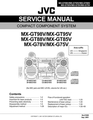
SlideShare a Scribd company logo
1 of 65
Download to read offline
SERVICE MANUAL
COMPACT COMPONENT SYSTEM
No.21026
Sep. 2001
COPYRIGHT 2001 VICTOR COMPANY OF JAPAN, LTD.
MX-GT98V/MX-GT95V
MX-GT88V/MX-GT85V
MX-G78V/MX-G75V
Safety precautions
Important for laser products
Preventing static electricity
Disassembly method
Adjustment method
1-2
1-3
1-4
1-5
1-29
Flow of functional operation
until TOC read
Maintenance of laser pickup
Replacement of laser pickup
Description of major ICs
1-33
1-34
1-34
1-35~49
Contents
(No MIC jack and MIC LEVEL volume for UN ver.)
MX-GT98V/MX-GT95V/MX-GT88V
MX-GT85V/MX-G78V/MX-G75V
COMPACT
DIGITAL VIDEO
COMPACT
DIGITAL AUDIO
Area suffix
US -------- Singapore
UN --------------Asean
SP-MXGT98V
SP-MXGT95V
SP-MXGT98V
SP-MXGT95V
CA-MXGT98V
CA-MXGT95V
MX-GT98V/MX-GT95V/MX-GT88V
MX-GT85V/MX-G78V/MX-G75V
1-2
1. This design of this product contains special hardware and many circuits and components specially for safety
purposes. For continued protection, no changes should be made to the original design unless authorized in
writing by the manufacturer. Replacement parts must be identical to those used in the original circuits. Services
should be performed by qualified personnel only.
2. Alterations of the design or circuitry of the product should not be made. Any design alterations of the product
should not be made. Any design alterations or additions will void the manufacturer's warranty and will further
relieve the manufacture of responsibility for personal injury or property damage resulting therefrom.
3. Many electrical and mechanical parts in the products have special safety-related characteristics. These
characteristics are often not evident from visual inspection nor can the protection afforded by them necessarily
be obtained by using replacement components rated for higher voltage, wattage, etc. Replacement parts which
have these special safety characteristics are identified in the Parts List of Service Manual. Electrical
components having such features are identified by shading on the schematics and by ( ) on the Parts List in
the Service Manual. The use of a substitute replacement which does not have the same safety characteristics
as the recommended replacement parts shown in the Parts List of Service Manual may create shock, fire, or
other hazards.
4. The leads in the products are routed and dressed with ties, clamps, tubings, barriers and the like to be
separated from live parts, high temperature parts, moving parts and/or sharp edges for the prevention of
electric shock and fire hazard. When service is required, the original lead routing and dress should be
observed, and it should be confirmed that they have been returned to normal, after re-assembling.
5. Leakage current check (Electrical shock hazard testing)
After re-assembling the product, always perform an isolation check on the exposed metal parts of the product
(antenna terminals, knobs, metal cabinet, screw heads, headphone jack, control shafts, etc.) to be sure the
product is safe to operate without danger of electrical shock.
Do not use a line isolation transformer during this check.
Plug the AC line cord directly into the AC outlet. Using a "Leakage Current Tester", measure the leakage
current from each exposed metal parts of the cabinet, particularly any exposed metal part having a return
path to the chassis, to a known good earth ground. Any leakage current must not exceed 0.5mA AC (r.m.s.).
Alternate check method
Plug the AC line cord directly into the AC outlet. Use an AC voltmeter having, 1,000 ohms per volt or more
sensitivity in the following manner. Connect a 1,500 10W resistor paralleled by a 0.15 F AC-type capacitor
between an exposed metal part and a known good earth ground.
Measure the AC voltage across the resistor with the AC
voltmeter.
Move the resistor connection to each exposed metal part,
particularly any exposed metal part having a return path to
the chassis, and measure the AC voltage across the resistor.
Now, reverse the plug in the AC outlet and repeat each
measurement. Voltage measured any must not exceed 0.75 V
AC (r.m.s.). This corresponds to 0.5 mA AC (r.m.s.).
1.This equipment has been designed and manufactured to meet international safety standards.
2. It is the legal responsibility of the repairer to ensure that these safety standards are maintained.
3. Repairs must be made in accordance with the relevant safety standards.
4. It is essential that safety critical components are replaced by approved parts.
5. If mains voltage selector is provided, check setting for local voltage.
Good earth ground
Place this
probe on
each exposed
metal part.
AC VOLTMETER
(Having 1000
ohms/volts,
or more sensitivity)
1500 10W
0.15 F AC TYPE
!
Burrs formed during molding may
be left over on some parts of the
chassis. Therefore, pay attention to
such burrs in the case of
preforming repair of this system.
In regard with component parts appearing on the silk-screen printed side (parts side) of the PWB diagrams, the
parts that are printed over with black such as the resistor ( ), diode ( ) and ICP ( ) or identified by the " "
mark nearby are critical for safety.
When replacing them, be sure to use the parts of the same type and rating as specified by the manufacturer.
(Except the J&C version)
MX-GT98V/MX-GT95V/MX-GT88V
MX-GT85V/MX-G78V/MX-G75V
1-3
Important for laser products
1.CLASS 1 LASER PRODUCT
2.DANGER : Invisible laser radiation when open and inter
lock failed or defeated. Avoid direct exposure to beam.
3.CAUTION : There are no serviceable parts inside the
Laser Unit. Do not disassemble the Laser Unit. Replace
the complete Laser Unit if it malfunctions.
4.CAUTION : The compact disc player uses invisible laser
radiation and is equipped with safety switches which
prevent emission of radiation when the drawer is open and
the safety interlocks have failed or are defeated. It is
dangerous to defeat the safety switches.
5.CAUTION : If safety switches malfunction, the laser is able
to function.
6.CAUTION : Use of controls, adjustments or performance of
procedures other than those specified herein may result in
hazardous radiation exposure.
VARNING : Osynlig laserstrålning är denna del är öppnad
och spårren är urkopplad. Betrakta ej strålen.
VARO : Avattaessa ja suojalukitus ohitettaessa olet
alttiina näkymättömälle lasersäteilylle.Älä katso
säteeseen.
ADVARSEL : Usynlig laserstråling ved åbning , når
sikkerhedsafbrydere er ude af funktion. Undgå
udsættelse for stråling.
ADVARSEL : Usynlig laserstråling ved åpning,når
sikkerhetsbryteren er avslott. unngå utsettelse
for stråling.
Position of labels
WARNING LABEL
! CAUTION Please use enough caution not to
see the beam directly or touch it
in case of an adjustment or operation
check.
DANGER : Invisibie laser radiation
when open and interlock or
defeated.
AVOID DIRECT EXPOSURE TO
BEAM (e)
VARNING : Osynlig laserstrålning
är denna del är öppnad och spårren
är
urkopplad. Betrakta ej strålen.
(s)
VARO : Avattaessa ja suojalukitus
ohitettaessa olet alttiina
näkymättömälle lasersäteilylle.Älä
katso säteeseen. (d)
ADVARSEL :Usynlig laserstråling
ved åbning , når
sikkerhedsafbrydere er ude af
funktion. Undgå udsættelse for
stråling. (f)
CLASS 1
LASER PRODUCT
CLASS 1
LASER PRODUCT
MX-GT98V/MX-GT95V/MX-GT88V
MX-GT85V/MX-G78V/MX-G75V
1-4
Preventing static electricity
1. Grounding to prevent damage by static electricity
Electrostatic discharge (ESD), which occurs when static electricity stored in the body, fabric, etc. is discharged,
can destroy the laser diode in the traverse unit (optical pickup). Take care to prevent this when performing repairs.
2. About the earth processing for the destruction prevention by static electricity
In the equipment which uses optical pick-up (laser diode), optical pick-up is destroyed by the static electricity of
the work environment.
Be careful to use proper grounding in the area where repairs are being performed.
2-1 Ground the workbench
Ground the workbench by laying conductive material (such as a conductive sheet) or an iron plate over
it before placing the traverse unit (optical pickup) on it.
2-2 Ground yourself
Use an anti-static wrist strap to release any static electricity built up in your body.
3. Handling the optical pickup
1. In order to maintain quality during transport and before installation, both sides of the laser diode on the
replacement optical pickup are shorted. After replacement, return the shorted parts to their original condition.
(Refer to the text.)
2. Do not use a tester to check the condition of the laser diode in the optical pickup. The tester's internal power
source can easily destroy the laser diode.
4. Handling the traverse unit (optical pickup)
1. Do not subject the traverse unit (optical pickup) to strong shocks, as it is a sensitive, complex unit.
2. Cut off the shorted part of the flexible cable using nippers, etc. after replacing the optical pickup. For specific
details, refer to the replacement procedure in the text. Remove the anti-static pin when replacing the traverse
unit. Be careful not to take too long a time when attaching it to the connector.
3. Handle the flexible cable carefully as it may break when subjected to strong force.
4. It is not possible to adjust the semi-fixed resistor that adjusts the laser power. Do not turn it
Conductive material
(conductive sheet) or iron plate
(caption)
Anti-static wrist strap
Attention when traverse unit is decomposed
1. Remove the disk stopper and T. bracket on the CD changer mechanism
assembly.
2. Disconnect the harness from connector on the CD motor board.
3. CD traverse unit is put up as shown in Fig.1.
4. Solder is put up before the card wire is removed from connector CN601
on the CD servo control board as shown in Fig. 2.
(When the wire is removed without putting up solder, the CD pick-up
assembly might destroy.)
5. Please remove solder after connecting the card wire with CN601 when
you install picking up in the substrate.
*Please refer to "Disassembly method" in the text for pick-up and how to
detach the CD traverse mechanism.
Soldering
Fig.1
Fig.2
CD changer
mechanism
assembly
CD traverse
unit
Flexible cable
MX-GT98V/MX-GT95V/MX-GT88V
MX-GT85V/MX-G78V/MX-G75V
1-5
Remove the six screws A on the back of the body.
Remove the two screws B on both sides of the
body.
Remove the metal cover from the body by lifting the
rear part of the cover.
1.
2.
3.
Disassembly method
<Main body>
Removing the metal cover
(See Fig.1 to 3)
Do not break the front panel tab fitted to
the metal cover.
CAUTION: Fig.1
Fig.2
Fig.3
A
AA
Metal cover
Metal cover
B
Metal cover
B
MX-GT98V/MX-GT95V/MX-GT88V
MX-GT85V/MX-G78V/MX-G75V
1-6
Prior to performing the following procedure, remove
the metal cover.
Disconnect the wire from connector CN705 on the
amplifier board.
Remove the plastic rivet attaching the main board to
the front assembly on the right side of the body.
Disconnect the card wire from connector CN561 on
the main board.
Remove the two screws C on the upper side of the
body and the two screws D on the back of the rear
panel.
Pull both the rear panel and the front panel assembly
to the outside, then remove the CD changer
mechanism assembly by lifting the rear part of the
assembly.
1.
2.
3.
4.
5.
Disconnect the card wire from connector CN504 on
the inner side of the main board on the right side of
the body. Remove the CD mechanism assembly.
6.
Removing the CD changer mechanism
assembly (See Fig.4 and 6)
Prior to performing the following procedure, remove
the metal cover and the CD changer mechanism
assembly.
Turn over the CD changer mechanism assembly and
remove the two screws E attaching the fan.
1.
Removing the fan (See Fig.7)
To prevent damage to the CD fitting, be
sure to pull both the rear panel and the
front panel assembly enough to remove
the CD changer mechanism assembly.
CAUTION:
At this point, one card wire on the
underside of the CD mechanism
assembly is still connected.
REFERENCE:
Fig.4
Fig.5
Fig.6
Fig.7
Front panel assembly
CC
CD changer
mechanism assembly
Rear panel
Main board
CN561
CN504
CD changer mechanism assembly
DMain board
CN561
Front panel assembly
Rear panel
CD changer mechanism assembly Front panel assembly
Amplifier board
CN705
CN504
Fan
EE
CD changer mechanism assembly
Rear panel
Plastic rivet
MX-GT98V/MX-GT95V/MX-GT88V
MX-GT85V/MX-G78V/MX-G75V
1-7
Prior to performing the following procedure, remove
the metal cover and CD changer mechanism
assembly.
Disconnect the card wires from connector CN870,
CN871 and CN315 on the main board respectively.
Remove the wire clamp and disconnect the wire from
connector CN703 on the amplifier board.
Disconnect the wire from connector CN220 on the
transformer board.
Remove the two screws F on the bottom of the
body.
Release the two joints a on the lower right and left
sides of the body using a screwdriver, and remove
the front panel assembly toward the front.
1.
2.
3.
4.
5.
Removing the front panel assembly
(See Fig.8 to 11)
Fig.9
Fig.10
Fig.11
F
(Bottom)
Joint a
Joint a
Front panel assembly
Fig.8
Wire clampAmplifier board
CN703
Main board
CN870
CN871
CN315
Transformer board
CN220
Front panel
assembly
MX-GT98V/MX-GT95V/MX-GT88V
MX-GT85V/MX-G78V/MX-G75V
1-8
Prior to performing the following procedure, remove
the metal cover.
Disconnect the card wire from connector CN1 on the
tuner board on the right side of the body.
Remove the plastic rivet fixing the tuner board.
Remove the two screws G on the back of the body.
1.
2.
3.
Removing the tuner board
(See Fig.12)
Prior to performing the following procedure, remove
the metal cover and the CD changer mechanism
assembly.
Remove the screw H attaching the rear cover on the
back of the body.
Push each tab of the four joints b in the direction of
the arrow and release.
Remove the fifteen screws G attaching the rear
panel.
Disengage the joints c on each lower side of the rear
panel using a screwdriver and remove the rear panel
backward.
1.
2.
3.
4.
Removing the rear cover / rear panel
(See Fig.13 to 16)
Fig.12
Fig.13
Fig.14
Fig.15Fig.16
CN1
Plastic rivet
Tuner board
Rear panel
Rear panelH
G
Joint b
Joint b
Rear cover
Rear panel
G
G
G G
G
Joint cJoint c Rear panel Rear panel
G
MX-GT98V/MX-GT95V/MX-GT88V
MX-GT85V/MX-G78V/MX-G75V
1-9
Prior to performing the following procedure, remove
the metal cover, the CD changer mechanism
assembly, the rear panel and the antenna board.
Disconnect the card wires from connector CN870,
CN871 and CN315 on the main board.
Disconnect the wires from connector CN704 and
CN706 on the amplifier board.
Remove the screw I attaching the main board on
the right side ofthe body.
Disconnect connector CN211 and CN212 on the
main board from the regulator board.
1.
2.
3.
4.
Removing the main board
(See Fig.17 and 18)
Prior to performing the following procedure, remove
the metal cover, the CD changer mechanism
assembly and the rear panel.
Disconnect connector CN217 on the speaker board
from the regulator board.
1.
Removing the speaker board
(See Fig.19)
It is not necessary to remove the main
board.
REFERENCE:
Fig.17
Fig.18
Fig.19
Front panel assembly
Amplifier board
CN704
CN706
Main board
CN870
CN871
CN315
Main board
Front panel assembly
I CN211
CN212
Regulator board
Regulator board
CN217
Speaker board
MX-GT98V/MX-GT95V/MX-GT88V
MX-GT85V/MX-G78V/MX-G75V
1-10
Prior to performing the following procedure, remove
the metal cover, the CD changer mechanism
assembly and the rear panel.
Disconnect the wires from connector CN703, CN704
and CN706 on the amplifier board respectively.
Remove the two wire clamps attaching the wire to
the amplifier board and the voltage board.
Disconnect connector CN215 on the amplifier board
and CN216 on the voltage board from the regulator
board (The heat sink will be detached at once).
Remove the four screws J attaching the amplifier
board to the heat sink.
Remove the two screws K, the board bracket and
the voltage board.
1.
2.
3.
4.
5.
Removing the amplifier board / voltage
board / heat sink (See Fig.21 and 22)
Prior to performing the following procedure, remove
the metal cover, the CD changermechanism
assembly and the rear panel.
Remove a wire clamp on the power board.
Disconnect the wire from connector CN218, CN219
and CN250 on the power board.
Disconnect connector CN251 on the power board
from the regulator board.
1.
2.
3.
Removing the power board (See Fig.20)
It is not necessary to remove the power
board.
REFERENCE:
Fig.21
Fig.20
Fig.22
Amplifier board
CN704
CN706
CN216
Regulator board
CN215
Wire clamp
Wire clamp
CN703
Voltage board
Amplifier board
Heat sink
Voltage board
J
J
K
CN218
Power board
CN219
Wire clamp
CN251
CN250
MX-GT98V/MX-GT95V/MX-GT88V
MX-GT85V/MX-G78V/MX-G75V
1-11
Prior to performing the following procedure, remove
the metal cover, the CD changer mechanism
assembly and the rear panel.
Disconnect the wires from connector CN218 and
CN219 on the power board.
Disconnect the wire from connector CN204 on the
regulator board.
Release the wire from the stopper on the regulator
board.
Remove the four screws L attaching the transformer
assembly.
1.
2.
3.
4.
Removing the power transformer
assembly (See Fig.23 and 24)
Prior to performing the following procedure, remove
metal cover, CD changer mechanism assembly, rear
panel, antenna board, main board, amplifier board,
voltage board, power board and speaker board.
Disconnect the wire from connector CN204 on the
regulator board.
Release the wire from the stopper on the regulator
board.
Remove the two screws M attaching the regulator
board.
1.
2.
3.
Removing the regulator board
(See Fig.25)
Prior to performing the following procedure, remove
the metal cover, the CD changer mechanism
assembly and the rear panel.
Disconnect the wire from connector CN250 on the
power board.
Remove the wire clamp from the power board.
Move the power cord stopper upward and pull out it
from the base chassis.
1.
2.
3.
Removing the power cord (See Fig.26)
Fig.23
Fig.24
Fig.25
Fig.26
CN219
Regulator board
CN204
Power transformer assembly
Power transformer
assembly Regulator board
CN204
L L
M
M
Power transformer assembly
Power board
CN218
Stopper
Regulator board
CN204
Stopper
Power board
CN250
Power cord stopper
Wire clampBase chassis
MX-GT98V/MX-GT95V/MX-GT88V
MX-GT85V/MX-G78V/MX-G75V
1-12
<Front panel assembly>
Prior to performing the following procedure, remove
the metal cover, the CD changer mechanism
assembly and the front panel assembly.
Disconnect the card wire from connector CN306 on
the head amplifier & mechanism control board.
Remove the seven screws N attaching the cassette
mechanism assembly.
1.
2.
Removing the cassette mechanism
assembly (See Fig.27)
Remove the four screws O attaching the stay
bracket.
Disconnect the card wires from connector CN316
and CN880 on the display system control board.
Remove the six screws P attaching the display
system control board.
If necessary, disconnect the wire from connector
CN911 on the front side of the display system control
board and unsolder FW915.
1.
2.
3.
4.
Removing the display system control
board (See Fig.28 to 30)
Remove the three screws Q attaching the CD eject
board.
If necessary, unsolder FW915 on the CD eject
board.
1.
2.
Removing the CD eject board
(See Fig.30 and 31)
Fig.27
Head amplifier
& mechanismcontrol board
CN306 N
N
N
N
Cassette mechanism
assembly
Fig.28
Fig.29
Fig.30Fig.31
O
Display system control board Stay bracket
P
P
P
P
CN316
CN880
FW915
(Solding)
P
Display system control board
FW915
FW915
CD eject board
CN911
Display system control board
CD eject board
FW915
(Solding)
Q
Q
MX-GT98V/MX-GT95V/MX-GT88V
MX-GT85V/MX-G78V/MX-G75V
1-13
Prior to performing the following procedure, remove
the display system control board.
Pull out the preset knob on the front panel.
Remove the four screws R attaching the preset /
tuning switch board.
If necessary, unsolder FW901 on the preset / tuning
switch board.
1.
2.
3.
Removing the preset / tuning switch
board (See Fig.32 and 33)
Prior to performing the following procedure, remove
the display system control board and the preset /
tuning switch board.
Pull out the volume knob on the front panel and
remove the nut. Pull out the surround mode knob,
the mic level knob and the surround woofer level
knob toward the front.
Remove the thirteen screws S attaching the
operation switch board. (CA-MXG75V / MXG78V,
CA-MXGT85V / MXGT88V)
Remove the twelve screws S attaching the
operation switch board. (CA-MXGT95V / MXGT98V)
Release each tab of the seven joints g retaining the
operation switch board.
1.
2.
3.
Removing the operation switch board
(See Fig.33 and 34)
Fig.32
Fig.33
Fig.34
Preset / tuning switch board
R
R
Volume knob Nut
Surround woofer
level knob
Surround mode knobPreset knob
S
SSSS
S
S
Joint g
Joint g
Joint g
Joints g
Joints g
Operation
switch board
Fig.34
S
SSSS
S
S
Joint g
Joint g
Joint g
Joints g
Joints g
Operation
switch board
Mic level knob
CA-MXG75V / MXG78V
CA-MXGT85V / MXGT88V
(CA-MXGT95V / MXGT98V)
MX-GT98V/MX-GT95V/MX-GT88V
MX-GT85V/MX-G78V/MX-G75V
1-14
Remove the four screws A attaching the front panel
on the front of the body.
Pull out the front panel toward the front and
disconnect the wire from the two speaker terminals
of the speaker (tweeter) on the back of the front
panel.
1.
2.
<Speaker section>
[for MX-GT98V/MX-GT95V]
Removing the front panel
(See Fig.1 and 2)
Prior to performing the following procedures, remove
the front panel.
Remove the two screws B attaching the speaker
(tweeter) on the back of the front panel.
1.
Removing the speaker (tweeter)
(See Fig.3)
Prior to performing the following procedures, remove
the front panel.
Remove the six screws C attaching the sub panel
on the back of the front panel.
Pull out the sub panel toward the front.
1.
2.
Removing the sub panel (See Fig.4)
Fig.1
Fig.2
Fig.3
Fig.4
A
A
A
A
B
Sub panel
Speaker (tweeter)
C
C
Speaker (tweeter)
Speaker terminals
C
Speaker (tweeter)
Front panel
Front panel
Front panel
Front panel
MX-GT98V/MX-GT95V/MX-GT88V
MX-GT85V/MX-G78V/MX-G75V
1-15
Prior to performing the following procedures, remove
the front panel.
Remove the four screws E attaching the speaker
(squawker) on the front of the body.
Disconnect the wire from the two speaker terminals
of the speaker (squawker).
1.
2.
Removing the speaker (squawker)
(See Fig.5)
Prior to performing the following procedures, remove
the front panel.
Remove the eight screws D attaching the punch
panel on the front of the body.
Remove the six screws F attaching the speaker
(woofer) on the front of the body.
Remove the speaker (woofer) toward the front and
disconnect the wire from the two speaker terminals.
1.
2.
3.
Removing the speaker (woofer)
(See Fig.6 and 7)
Remove the four screws G attaching the duct on the
upper side of the body.
Move the duct upwards and pull out backward.
1.
2.
Removing the duct (See Fig.8)
Fig.5
Fig.6
Fig.7Fig.8
D
Speaker (squawker)
D
E
E
Speaker (woofer)
F
Front panel
G
Duct
G
Speaker (squawker)
Punch panel
F
MX-GT98V/MX-GT95V/MX-GT88V
MX-GT85V/MX-G78V/MX-G75V
1-16
Remove the four screws A attaching the front panel
on the front of the body.
Pull out the front panel toward the front.
1.
2.
[for MX-GT88V/MX-GT85V]
Removing the front panel (See Fig.1)
Prior to performing the following procedures, remove
the front panel.
Remove the two screws B attaching the speaker
(tweeter) on the front of the body.
Disconnect the wire from two speaker terminals of
the speaker (tweeter).
1.
2.
Removing the supeaker (tweete)
(See Fig.2)
Prior to performing the following procedures, remove
the front panel.
Remove the four screws C attaching the speaker
(squawker) on the front of the body.
Disconnect the wire from the two speaker terminals
of the speaker (squawker).
1.
2.
Removing the speaker (squawker)
(See Fig.3)
Fig.1
Fig.2
Fig.3
A A
AA
Front panel
B
Speaker (squawker)
Spealer (tweeter)
Speaker (squawker)
C
C
MX-GT98V/MX-GT95V/MX-GT88V
MX-GT85V/MX-G78V/MX-G75V
1-17
Prior to performing the following procedures, remove
the front paenel.
Remove the six screws D attaching the punch panel
on the front of the body.
Remove the four screws E attaching the speaker
(woofer) on the front of the body.
Pull out the speaker (woofer) toward the front and
disconnect the wire from the two speaker terminals.
1.
2.
3.
Removing the speaker (woofer)
(See Fig.4 and 5)
Prior to performing the following procedures, remove
the front panel.
Remove the six screws F attaching the sub panel on
the back of the front panel.
Remove the sub panel toward the front.
1.
2.
Removing the sub panel (See Fig.6 )
Remove the four screws G attaching the duct on the
upper side of the body.
Move the duct upwards and pull out backward.
1.
2.
Removing the duct (See Fig.7)
Fig.4
Fig.5
Fig.6Fig.7
D
Punch panel
D
EE
Speaker (woofer)
Sub panel
FFFront paenl
G
Duct
G
Front paenl
MX-GT98V/MX-GT95V/MX-GT88V
MX-GT85V/MX-G78V/MX-G75V
1-18
Remove the six screws A on the side of the body.1.
Removing the side cover (See Fig.1)
Prior to performing the following procedure, remove
the side cover.
Remove the four screws B on the side of the body.
Disconnect the red and black wires from the speaker
terminals on the squawker speaker.
1.
2.
Removing the squawker speaker
(See Fig.2)
Prior to performing the following procedure, remove
the side cover.
Pull out the saran net toward the front while
disengaging the four joints a.
Remove the two screws C and D respectively.
Remove the front cover toward the front and
disconnect the yellow and black wires from the two
tweeter speaker terminals.
1.
2.
3.
Removing the front cover (See Fig.3 to 5)
[for MX-G78V/MX-G75V]
Fig.1
Fig.2
Fig.3
A
A
A
A
Side cover
B
Squawker speaker
B
Joints a
Joints a
Saran net
Fig.4
Front cover
C C
DD
MX-GT98V/MX-GT95V/MX-GT88V
MX-GT85V/MX-G78V/MX-G75V
1-19
Prior to performing the following procedure, remove
the side cover and the front cover.
Remove the four screws E on the front of the body.
Pull out the woofer speaker toward the front and
disconnect the wire (yellow and black,blue and
black) from the two speaker terminals.
1.
2.
Removing the woofer speaker (See Fig.6)
Prior to performing the following procedure, remove
the side cover and the front cover.
Remove the two screws F attaching the tweeter
speaker on the back of the front cover.
1.
Removing the tweeter speaker
(See Fig.7)
Fig.5
Fig.6
Fig.7
Woofer speaker
E
Tweeter speaker
E
Tweeter speaker
Front cover
F
MX-GT98V/MX-GT95V/MX-GT88V
MX-GT85V/MX-G78V/MX-G75V
1-20
Removing the CD Servo control board
(See Fig.1)
Removing the CD tray assembly
(See Fig.2~4)1.
2.
3.
4.
5.
6.
7.
8.
9.
Remove the front panel assembly.
Remove the CD changer mechanism assembly.
Remove the CD Servo control board.
Remove the screw B' retaining the lod stopper.
From the T.bracket section "b" and clamper base
section "c" , remove both of the edges fixing the
rod(See Fig.2 and 3).
Remove the screw B retaining the disc stopper
(See Fig.3).
Remove the three screws C retaining the T.bracket
(See Fig.3).
Remove the screw D retaining the clamper assembly
(See Fig.3).
From the left side face of the chassis assembly, remove
the one screw E retaining both of the return spring and
lock lever(See Fig. 4).
By removing the pawl at the section "d" fixing the return
spring, dismount the return spring(See Fig.4).
Remove the three lock levers(See Fig.4).
10.
11.
Fig.1
Fig.2
Fig.3
Fig.4
1.Remove the metal cover.
2.Remove the CD changer mechanism assembly.
3.From bottom side the CD changer mechanism assembly,
remove the four screws A retaining the CD servo control
board.
4.Absorb the four soldered positions "a" of the right and
left motors with a soldering absorber.
5.Pull out the earth wire on the CD changer mechanism
assembly.
6.Disconnect the connector CN854 on the CD servo
control board.
7.Disconnect the card wire CN601 and the connector
CN801 on the CD servo control board.
CN601
CN801
b
c
E
Rod
T.Braket
Clamper base
T.Braket Disc stopper
Lod stopper
(C/J version only)
Clamper ass'y
b
a
C C
B'
D
C
d
Lock lever
Return spring
CD servo control board
CN651
CN854
a
a
A
A
AA
CN151
CN652
B
Earth
wire
MX-GT98V/MX-GT95V/MX-GT88V
MX-GT85V/MX-G78V/MX-G75V
1-21
11.
12.
Check whether the lifter unit stopper has been caught
into the hole at the section "e" of CD tray assembly as
shown in Fig.5.
Make sure that the driver unit elevator is positioned as
shown in Fig.6 from to the second or fifth hole on the
left side face of the CD changer mechanism assembly.
Fig.5
Fig.7
Fig.6
Fig.8 Fig.9
[Caution] In case the driver unit elevator is not at above
position, set the elevator to the position as
shown in Fig.7 by manually turning the pulley
gear as shown in Fig.8.
13.
14.
15.
Manually turn the motor pulley in the clockwise
direction until the lifter unit stopper is lowered from the
section "e" of CD tray assembly(See Fig.8).
Pull out all of the three stages of CD tray assembly in
the arrow direction "f" until these stages stop
(See Fig.6).
At the position where the CD tray assembly has
stopped, pull out the CD tray assembly while pressing
the two pawls "g and g' " on the back side of CD tray
assembly(See Fig.9). In this case, it is easy to pull out
the assembly when it is pulled out first from the stage
CD tray assembly.
CD 3
CD 2
CD 1
CD tray
assembly
e
Drive unit of elevator
CD tray assembly
f
Refer to Fig.7 Pawl
Chassis assembly
Pulley gear
Motor pulley
Pawl ,
CD tray assembly
Stopper
g
g g'
MX-GT98V/MX-GT95V/MX-GT88V
MX-GT85V/MX-G78V/MX-G75V
1-22
Removing the CD loading mechanism
assembly(See Fig.10)
1.
2.
While turning the cams R1 and R2 assembly in the
arrow direction "h" ,align the shaft "i" of the CD loading
mechanism assembly to the position shown in Fig.10.
Remove the four screws F retaining the CD loading
mechanism assembly.
Removing the CD traverse mechanism
(See Fig.11 and 12 )
1.
2.
For dismounting only the CD traverse mechanism
without removing the CD loading mechanism assembly,
align the shaft "j" of the CD loading mechanism
assembly to the position shown Fig.11 while turning the
cam R1 and R2 assembly in the arrow direction "k" .
By raising the CD loading mechanism assembly in the
arrow direction "l", remove the assembly from the lifter
unit
Fig.10
Fig.12
Fig.11
Fig.13
Removing the CD pick unit
(See Fig.13 )
1.
2.
3.
4.
Move the cam gear in the arrow direction "m" . Then,
the CD pickup unit will be moved in the arrow direction
"n" .
According to the above step, shift the CD pickup unit to
the center position.
While pressing the stopper retaining the shaft in the
arrow direction "o" , pull out the shaft in the arrow
direction "p".
After dismounting the shaft from the CD pickup unit,
remove the CD pickup unit
Cams R1, R2 assembly
i
CD loading mechanism assembly
h
F
F
F F
Arrow
Lifter unit
CD traverse mechanism
l
n
o p
m
Arrow
Cam R1, R2 assembly
kArrow
j
CD Pickup unit
CD loading
mechanism
Shaft
Cam gear
ShaftShaft
Stopper Stopper
MX-GT98V/MX-GT95V/MX-GT88V
MX-GT85V/MX-G78V/MX-G75V
1-23
Removing the try select switch board
(See Fig.14)
1.
2.
Remove the two screws G retaining the tray select
switch board.
Disconnect the tray select switch board from connector
CN804 on the CD servo control board.
Fig.15
Fig.14
Fig.16
Removing the cam unit
(See Fig.15 ~17 )
1.
2.
3.
4.
5.
Remove the CD loading mechanism assembly.
While turning the cam gear "q", align the Paul "r"
position of the drive unit to the notch position(Fig.16) on
the cam gear "q".
Pull out the drive unit and cylinder gear(See Fig.17).
While turning the cam gear "q", align the Paul "s"
position of the select lever to the notch position(Fig.18)
on the cam gear "q".
Remove the four screws H retaining the cam unit(cam
gear "q" and cams R1/R2 assembly)(See Fig.18).
Cam gear qDrive unit
r
G
H
J
H
Chassis assembly
Tray select
switch board
CN854
CN851
CN804
Cylinder gear
Drive unit
Fig.17
Select lever
Cams R1, R2 assembly
Cam unitCam gear q
s
MX-GT98V/MX-GT95V/MX-GT88V
MX-GT85V/MX-G78V/MX-G75V
1-24
Fig.18
Fig.20Fig.19
Fig.21
[Note] When the chassis assembly is turned over under
the conditions wherein the gear bracket and belt
have been removed, then the pulley gear as well
as the gear, etc. constituting the gear unit can
possibly be separated to pieces. In such a case,
assemble these parts by referring to the assembly
and configuration diagram in Fig. 21.
Removing the actuator motor and belt
(See Fig.18~21)
1.
2.
3.
4.
5.
Remove the two screws I retaining the gear bracket
(See Fig.18).
While pressing the pawl "t" fixing the gear bracket in the
arrow direction, remove the gear bracket
(See Fig.18).
From the notch "u section" on the chassis assembly
fixing the edge of gear bracket, remove and take out the
gear bracket(See Fig. 19).
Remove the belts respectively from the right and left
actuator motor pulleys and pulley gears(See Fig. 18).
After turning over the chassis assembly, remove the
actuator motor while spreading the four pawls "v" fixing
the right and left actuator motors in the arrow
direction(See Fig. 20).
Pulley gear
Belt
Motor pulley
BeltPulley gear
Motor pulley
Gear bracket
t
I
I
Pawl
v
Actuator motor
v
Chassis assembly
u
Gear bracket
Pulley gear
Gear B
Cylinder gear
Gross gear U
Gear CGross gear L
Select gear
Gear B
Gear C
Pulley gear
Assembly and Configuration Diagram
MX-GT98V/MX-GT95V/MX-GT88V
MX-GT85V/MX-G78V/MX-G75V
1-25
Fig.22
[Caution] To reassemble the cylinder gear, etc.with the
cam unit (cam gear and cans R1/R2 assembly),
gear unit and drive unit, align the position of the
pawl "x" on the drive unit to that of the notch on
the cam gear "q". Then, make sure that the
gear unit is engaged by turning the cam gear
"q" (See Fig. 24).
Removing the cams R1/R2 assembly
and cam gear q(See Fig.22)
1.
2.
3.
4.
Remove the slit washer fixing the cams R1 and R2
assembly.
By removing the two pawls "w" fixing the cam R1,
separate R2 from R1.
Remove the slit washer fixing the cam gear "q".
Pull out the cam gear "q" from the C.G. base assembly.
Removing the C.G. base assembly
(See Fig.22 and 23)
Remove the three screws J retaining the C.G. base
assembly.
Fig.23
Slit washer
Pawl
Cam R2
Slit washer
Cam gear q
Cam switch board
C.G. base assembly
Cam R1
Pawl
Cam gear q
Notch
Cylinder
gear
Gear bracket
Cam R1, R2 assembly
Gear unit
Drive unit
xPawl
ww
J
MX-GT98V/MX-GT95V/MX-GT88V
MX-GT85V/MX-G78V/MX-G75V
1-26
< Cassette mechanism section >
Removing the playback,recording and eraser
heads (See Fig.1~3)
1. While shifting the trigger arms seen on the right
side of the head mount in the arrow direction,turn
the flywheel R in counterclockwise direction until
the head mount has gone out with a click
(See Fig. 1).
2. When the flywheel R is rotated in counterclockwise
direction, the playback / recording & eraser head will
be turned in counterclockwise direction from the
position in Fig.2 to that in Fig.3.
3. At this position, disconnect the flexible P.C.board
(outgoing from the playback head) from the
connector CN301 on the head amp. and mechanism
control P.C. board.
4. Remove the flexible P.C.board from the chassis
base.
5. Remove the spring "a" from behind the playback /
recording head.
6. Loosen the reversing azimuth screw retaining the
playback head.
7. Take out the playback head from the front of the
head mount.
8. The recording and eraser heads should also be
removed similarly according to Steps 1~7 above.
Reassembling the playback, recording
and eraser heads (See Fig.3)
1. Reassemble the playback head from the front of
the head mount to the position as shown in Fig.3.
2. Fix the reversing azimuth screw.
3. Set the spring a from behind the playback head.
4. Attach the flexible P.C.board to the chassis base
as shown in Fig.3.
5. The recording and eraser heads should also be
reassembled similarly according to Steps 1~4
above.
Cassette mechanism
Flywheel R
Trigger armHead mount
(Mechanism A side)
(Mechanism A side)
Playback/Recording &
eraser head
Flexible
P.C.board
Spring "a"
Trigger arm
Head amplifier & mechanism
control P.C. board
Flywheel R
CN301
Fig.1
Fig.2
Playback head Reversing azimuth
screw
Head
mount
Flexible
P.C.board
Spring "a"
FPC holder
Head amplifier &
mechanism control
P.C. board
CN302
(Mechanism B side)
Fig.3
MX-GT98V/MX-GT95V/MX-GT88V
MX-GT85V/MX-G78V/MX-G75V
1-27
Removing the head amp. and mechanism
control board (See Fig. 4)
1.Remove the cassette mechanism assembly.
2.After turning over the cassette mechanism
assembly,remove the five screws "A" retaining
the head amplifier & mechanism control board.
3.Disconnect the connectors CN303 on the board
and the connectors CN301 and on CN302 both
the right and left side reel pulse boards.
4.When necessary, remove the 4pin parallel
wire soldered to the main motor
Removing the capstan motor assembly
(See Fig.5 to 7)
1.Remove the six screws "B" retaining capstan
motor assembly (See Fig. 5).
2.While raising the capstan motor, remove the
capstan belts A and B respectively from the
motor pulley (See Fig. 6).
Caution 1: Be sure to handle the capstan
belts so carefully that these belts
will not be stained by grease and
other foreign matter. Moreover,
these belts should be hand while
referring to the capstan belt
hanging method.(See Fig.6 and 7)
Flexible
board
Flexible
board
CN302 CN301
CN303
Head amplifier &
mechanism control board
Capstan motor
assembly
Capstan
belt A
Capstan
belt B
Motor pulley
Capstan
belt A
Capstan
belt B
Capstan motor
A A A
AA
B B
BBBB
Fig.4
Fig.5
Fig.7 Fig.6
MX-GT98V/MX-GT95V/MX-GT88V
MX-GT85V/MX-G78V/MX-G75V
1-28
Removing the capstan motor (See Fig. 8)
From the joint bracket, remove the two screws "C"
retaining the capstan motor.
Removing the flywheel (See Fig. 9,10)
1.Remove the head amp. and mechanism control
P.C.Board.
2.Remove the capstan motor assembly.
3.After turning over the cassette mechanism, remove
the two slit washers "b" fixing the capstan shafts
R and L, and pull out the flywheels R and L respectively
from behind the cassette mechanism.
Removing the reel pulse board and solenoid
(See Fig. 11)
1.Remove the five pawls (c,d,e,f,g) retaining
the reel pulse P.C.Board.
2.From the surface of the reel pulse P.C.Board parts,
remove the two pawls "h" and "i" retaining the solenoid.
Capstan motor
Joint
bracket
Flywheel R Flywheel L
Slit
washer "a"
Slit
washer "b"
Reel pulse board
Solenoid
Solenoid
C
C
a b
c d e f g
h i
Fig.8
Fig.9
Fig.11
Fig.10
MX-GT98V/MX-GT95V/MX-GT88V
MX-GT85V/MX-G78V/MX-G75V
1-29
Adjustment method
Measurement instruments required
for adjustment
Measurement conditions
Power supply voltage
AC110/127/230-240V(50/60Hz): US,UN model
Measurement
output terminal : Speaker out
: TP101(Mesuring for TUNER/DECK/CD)
: Dummy load 6ohm
Radio input signal
AM modulation frequency : 400Hz
Modulation factor : 30%
FM modulation frequency : 400Hz
Frequency displacement : 22.5kHz
Frequency Range
AM 531kHz~1710kHz : US,UN model
FM 87.5MHz~108MHz
Standard measurement positions of volume
and switch
Power : Standby (Light STANDBY Indicator)
Sub woofer VOL. : Minimum
Sound mode : OFF
Main VOL. : 0 Minimum
Traverse mecha set position : Disc 1
Mic MIX VOL : MAX (Only US,UN ver.)
ECHO : OFF
Precautions for measurement
1. Apply 30pF and 33kohm to the IF sweeper output
side and 0.082 F and 100kohm in series to
the sweeper input side.
2. The IF sweeper output level should be made as
low as possible within the adjustable range.
3. Since the IF sweeper is a fixed device, there is
no need to adjust this sweeper.
4. Since a ceramic oscillator is used, there is no need
to perform any MPX adjustment.
5. Since a fixed coil is used, there is no need to adjust
the FM tracking.
6. The input and output earth systems are separated.
In case of simultaneously measuring the voltage
in both of the input and output systems with an
electronic voltmeter for two channels, therefore,
the earth should be connected particularly.
7. In the case of BTL connection amplifier, the minus
terminal of speaker is not for earthing. Therefore,
be sure not to connect any other earth terminal
to this terminal. This system is of an OTL system.
1. Low frequency oscillator,
This oscillator should have a capacity to output 0dBs
to 600ohm at an oscillation frequency of 50Hz-20kHz.
2. Attenuator impedance : 600ohm
3. Electronic voltmeter
4. Frequency counter
5. Wow flutter meter
6. Test tape
VT703L : Head azimuth
VT712 : For Tape speed and wow flutter ( 3kHz)
VT724 : For Reference level (1kHz)
VT703L : For Head angle(10kHz)
7. Blank tape
TAPE : AC-225,
8. Torque gauge : For play and back tension
Forward ; TW2111A, Reverse ; TW2121A
Fast Forward and Rewind ; TW2231A
9. Test disc
: CTS-1000(12cm),GRG-1211(8cm)
10. Jitter meter
MX-GT98V/MX-GT95V/MX-GT88V
MX-GT85V/MX-G78V/MX-G75V
1-30
Arrangement of adjusting positions
Cassette mechanism section (Mechanism A section) Cassette mechanism section (Back side)
Cassette Mechanism Unit Section
Head azimuth
adjusting screw
(Forward side)
Head azimuth
adjusting screw
(Reverse side)
Head azimuth
adjusting screw
(Forward side)
Head azimuth
adjusting screw
(Reverse side)
Playback
head
Playback, recording and eraser
heads or playback head
Tape speed ADJ
Bias ADJ L
Bias ADJ R
MX-GT98V/MX-GT95V/MX-GT88V
MX-GT85V/MX-G78V/MX-G75V
1-31
1.Playback the test tape VT703L.
2.With the playback mechanism or recording &
playback mechanism, adjust the head azimuth
screw so that the forward and reverse output
levels become maximum.After adjustment,lock
the head azimuth at least by half a turn.
3.In either case,this adjustment should be
performed in both the forward and reverse
directions with the head azimuth screw.
<Constant speed>
Adjust VR301 so that the frequency counter reading
becomes 3,000Hz 60Hz when playing back the
test tape VT712(3kHz)with the playback mechanism
or playback and recording mechanism after ending
forward winding of the tape.
Confirmation
of head angle
Confirmation
of tape speed
Test tape
:VT7036L
Measurement
output terminal
:Speaker terminal
Speaker R
(Load resistor:6 )
:Headphone terminal
Test tape
:VT712(3kHz)
Measurement
output terminal
:Headphone terminal
Maximum
output
Tape speed
of decks
(A and B)
:3,000Hz
60Hz
Adjust the head
azimuth screw
only when the
head has been
changed.
VR301
Items Measurement
conditions
Measurement method Standard
values
Adjusting
positions
Tape recorder section
Items Measurement
conditions
Measurement method Standard
values
Adjusting
positions
After setting to the double speed motor, confirm
that the frequency counter reading becomes
4,800+400/-300Hz when the test tape VT712
(3kHz) has been play back with the playback
mechanism.
When the test tape VT712(3kHz) has been played
back with the playback mechanism or recording and
playback mechanism at the beginning of forward
winding, the frequency counter reading of the
difference between both of the mechanisms should
be 6.0Hz or less.
When the test tape VT712(3kHz) has been played
back with the playback mechanism or recording and
playback mechanism at the beginning of forward
winding the frequency counter reading of wow &
flutter should be 0.25% or less(WRMS).
Double tape
speed
Difference
between the
forward and
reverse speed.
P.mecha and
R/P mecha
speed
Wow & flutter
Test tape
:VT712(3kHz)
Measurement
output terminal
:Speaker terminal
Speaker R
(Load resistance:6 )
measurement
output terminal
:Headphone terminal
Test tape
:VT712(3kHz)
Measurement
output terminal
:Headphone terminal
4,800+400/
-300Hz
60Hz or
less
with in
0.25%
JIS(WTD)
Playback
mechanism side
Both the playback
and recording &
playback
mechanism
Both the playback
and recording &
playback
mechanism
Reference values for confirmation items
MX-GT98V/MX-GT95V/MX-GT88V
MX-GT85V/MX-G78V/MX-G75V
1-32
Items Measurement
conditions
Measurement method Standard
values
Adjusting
positions
1.With the recording and playback mechanism,
load the test tapes(AC-225 to TYP ),and set the
mechanism to the recording and
pausing conditions in advance.
2.After connecting 100 in series to the recorder
head,measure the bias current with a valve
voltmeter at both of the terminals.
3.After resetting the [PAUSE] mode,start recording.
At this time,adjust VR101 for LcH and VR201 for
RcH so that the recording bias current values
become 4.0 A (TYP ).
1.With the recording and playback mechanism,load
the test tape(AC-225 to TYP ),and set the
mechanism to the recording and pausing condition
in advance.
2.While repetitively inputting the reference frequency
signal of 1kHz and 10kHz from OSC IN, record and
playback the test tape.
3.While recording and playing back the test tape in
TYP ,adjust VR101 for LcH and VR201 for RcH
so that the output deviation between 1kHz and
10kHz becomes -1dB 2dB.
Adjustment of
recording bias
current
(Reference
value)
Adjustment of
recording and
playback
frequency
characteristics
*Mode : Forward or
reverse mode
*Recording mode
*Test tape
: AC-225
Measurement output
terminal
:Both recording and
headphone terminals
Reference frequency
:1kHz and 10kHz
(REF:-20dB)
Test tape
:TYP AC-225
Measurement input
terminal
:OSC IN
AC-225
:4.20 A
Output
deviation
between
1kHz and
10kH
:-1dB 2dB
LcH
:VR101
RcH
:VR201
LcH
:VR101
RcH
:VR201
Electrical performance
Items Measurement
conditions
Measurement method Standard
values
Adjusting
positions
1.While changing over to and from BIAS 1 and 2,
confirm that the frequency is changed.
2.With the recording and playback mechanism.
load the test tape (AC-225 to TYP ),and set the
mechanism to the recording and pausing
conditions in advance.
3.Confirm that the BIAS TP frequency on the
P.C.board is 100kHz 6kHz.
1.With the recording and playback mechanism,
load the test tapes(AC-225 to TYP ),and set the
mechanism to the recording and pausing condition
in advance.
2.After setting to the recording conditions,connect
1M in series to the eraser head on the recording
and playback mechanism side,and measure the
eraser current from both of the eraser terminal.
Recording
bias frequency
Eraser current
(Reference
value)
*Recording and
playback side forward
or reverse
*Test tape
:TYP AC-225
*Measurement
terminal BIAS TP on
P.C.board
*Recording and
playback side forward
or reverse
*Recording mode
*Test tape
:AC-225
Measurement terminal
Both of the eraser
head
100kHz
+9kHz
-7kHz
TYP
:75mA
Reference values for electrical function confirmation items
MX-GT98V/MX-GT95V/MX-GT88V
MX-GT85V/MX-G78V/MX-G75V
1-33
Flow of functional operation until TOC read
Slider turns REST
SW ON.
Automatic tuning
of TE offset
Laser ON
Detection of disc
Automatic measurement of
Focus S-curve amplitude
Automatic tuning of
Focus offset
Disc is rotated
Focus servo ON
(Tracking servo ON)
Automatic tuning of
Tracking error balance
Automatic measurement of
Tracking error amplitude
Automatic tuning of
Focus error balance
Disc to be
braked to stop
Tracking
servo
on states
Tracking
servo
off states
Disc states
to rotate
TOC reading
finishes
Automatic measurement
of TE amplitude and
automatic tuning of
TE balance
500mv/div
2ms/div Fig.1
Approx.3secpin 25 of
IC601(TE)
Approx
1.8V
VREF
Tracking error waveform at TOC reading
Power ON Play Key
Confirm that the Focus error
S-cuve signal at the pin28 of
IC651 is approx.2Vp-p
Confirm that the signal from
pin24 IC651 is 0V as a
accelerated pulse during
approx.400ms.
Confirm the waveform of
the Tracking error signal.
at the pin 25 of IC601 (R604)
(See fig-1)
Automatic tuning of
Focus error gain
Automatic tuning of
Tracking error gain
TOC reading
Play a disc
Confirm the eys-pattern
at the lead of TP1
Confirm that the voltage at the pin5
of CN801 is "H""L""H".
Check Point
Check that the voltage at the
pin40 of IC651 is + 5V?
MX-GT98V/MX-GT95V/MX-GT88V
MX-GT85V/MX-G78V/MX-G75V
1-34
Turn off the power switch and, disconnect the
power cord from the ac outlet.
Replace the pickup with a normal one.(Refer
to "Pickup Removal" on the previous page)
Plug the power cord in, and turn the power on.
At this time, check that the laser emits for
about 3seconds and the objective lens moves
up and down.
Note: Do not observe the laser beam directly.
Play a disc.
Check the eye-pattern at TP1.
Finish.
Maintenance of laser pickup
(1) Cleaning the pick up lens
Before you replace the pick up, please try to
clean the lens with a alcohol soaked cotton
swab.
(2) Life of the laser diode
When the life of the laser diode has expired,
the following symptoms will appear.
1. The level of RF output (EFM output : ampli
tude of eye pattern) will below.
Is the level of
RFOUT under
1.25V 0.22Vp-p?
Replace it.
NO
YES
O.K
(3) Semi-fixed resistor on the APC PC board
The semi-fixed resistor on the APC printed circuit board which is attached to the pickup is used to adjust the laser
power. Since this adjustment should be performed to match the characteristics of the whole optical block, do not
touch the semi-fixed resistor.
If the laser power is lower than the specified value, the laser diode is almost worn out, and the laser pickup should
be replaced.
If the semi-fixed resistor is adjusted while the pickup is functioning normally, the laser pickup may be damaged
due to excessive current.
Replacement of laser pickup
MX-GT98V/MX-GT95V/MX-GT88V
MX-GT85V/MX-G78V/MX-G75V
1-35
1 2 3 4 5 6 7 8 9 10 11 12
131415161718192021222324
AMP
Pre
Source
CTRL
AMP
ALC
ALC
AMPAMP
EQ
CTRL ALC
REPPLE
REJ
Pre
Pre
L1 L2
R1 R2 NF2
NF1 OUT1
OUT2
EQ1
EQ2 CTL2
CTL1
RIN2
RIN1
RNF2
RNF1
ROUT2
ROUT1
LC LPF GND
EQ
CTL RF VCC
AN7345K (IC302) : PB/REC amp.
2. Pin Function
Pin
No. Symbol I/O Function FunctionI/OSymbol
Pin
No.
1
2
3
4
5
6
7
8
9
10
11
12
13
14
15
I
I
16
17
18
19
20
21
22
23
24 I
I
O
I
I
Playback amplifier output
I
I
I
RIN1
OUT1
1. Block diagram
Playback amplifier inputR1
R2 I Playback amplifier input
NF2 Playback amplifier negative feedback
OUT2 Playback amplifier output
EQ2 I Equlaizer
CTL2 I Pre Amplifier input swithing time
constant
RIN2 I Recording amplifier input
RNF2 I Recording amplifier negative feedback
ROUT2
O
Recording amplifier outputO
LC I ALC low cut
LPF I ALC low pass filter
GND I
Vcc Power supply
RF I Repple filter
EQCTL EQ control
ROUT1 O Recording amplifier output
RNF1 Recording amplifier negative feedback
I Recording amplifier input
CTL1 Pre amplifier input swithing control
EQ1 Equlayzer
Playback amplifier negative feedbackNF1
L2 I
L1
Playback amplifier input
Description of major ICs
MX-GT98V/MX-GT95V/MX-GT88V
MX-GT85V/MX-G78V/MX-G75V
1-36
1
2
3
4
5
6
7
8
9,10
11
12,13
14
15
16~19
20
21
22
23
24
25
26
27
28
29
30
31
32
33
34
35
36
37
38
39
40~41
42
43
44
45,46
47
48
49
50
KCMND
MSTAT
KCLK
DATAOUT
DATAIN
CK
BEAT
VDD
OSC2,1
VSS
XI,XO
MMOD
VREF-
KEY1~4
SLCKEY1
SLCKEY2
SLCKEY3
SPI
VREF+
MRDY
RESET
P OPEN
P CLOSE
VOLLED
MSI
ECHO2
ECHO1
REMIN
PHOTOA
PHOTOB
INH
RDSCLK
PRT
EXTCE
BASSVOL+/-
RDS-DATA
SPIA
SPIB
VOL+/-
MPX
FVOLDA
VOLCLK
BASSLED
SVC3 Serial data output
SVC3 status input input
SVC3 Serial clock input
SLC/TUNER data output
TUNER data input
SLC/TUNER clock
Beat cut signal output of TUNER
Power supply +5V
Oscillation terminal (8MHz)
Connect to GND
Sub clock (32.768kHz)
Connect to GND
Connect to GND
Key matrix input 1~4
Tape B playback/recording detect switch
Tape B playback detect switch
Tape A playback detect switch
SPI IN
AD port voltage reference
VC3 Ready
Reset signal input
Rolling panel open detection signal input
Rolling panel close detection signal input
LED Control signal output (VOL)
MS detector signal input
Echo ON/OFF(Not used)
Remote control signal input
Tape A mechanism running detection signal input
Tape B mechanism running detection signal input
Inhibit signal input
Clock signal input from IC3 (B/E/EN model)
Protector input
EXT IC Chip enable
Bass volume rotary encoder input(+/-)
RDS data input from IC3(B/E/EN model)
SPI Control A
SPI Control B
Volume rotary encoder input (+/-)
Stereo detect
Front volume data output
O
I
I
O
I
O
O
-
I/O
-
I/O
-
-
I
I
I
I
I
I
I
I
I
I
O
I
-
-
I
I
I
I
I
I
-
I
I
-
-
I
I
O
O
O
Pin No. Symbol I/O Function
MN101C35DEA (IC810) : System controller
Pin function (1/2)
Clock signal output to IC436
LED Control signal output (BASS)
MX-GT98V/MX-GT95V/MX-GT88V
MX-GT85V/MX-G78V/MX-G75V
1-37
51~63
64~87
88
89
90
91
92
93
94
95
96
97
98
99
100
G13~G1
P1~P24
SLCCE
AUX LED
DOORCL
DOOR OPEN
CDLED
TAPE LED
TU LED
SMUTE
BTU+
POUT
TUCE
VC3RESET
VPP
FL grid control signal output
FL segment control signal output
SLC Chip enable signal output to IC303,IC304
LED Control signal output (AUX)
Rolling panel motor control signal output
LED Control signal output (CD)
LED Control signal output (TAPE)
LED Control signal output (TUNER)
System mute control signal output
Tuner supply control
Power ON/OFF
TUNER Chip enable signal output
VC3 reset output
Power supply
O
O
O
O
O
O
O
O
O
O
O
O
O
O
-
Pin No. Symbol I/O Function
Pin function (2/2)
STROBE
DATA
CLOCK
Q1
Q2
Q3
Q4
Vss
Vdd
OUTPUT ENABLE
Q5
Q6
Q7
Q8
Q's
Qs
1
2
3
4
5
6
7
8
16
15
14
13
12
11
10
9
1.Pin layout
8-STAGE
SHIFT REGISTER
8-BIT
LATHES
3-STATE
OUTPUTS
1
2
3
15
Q1 Q8
10
9
DATA
CLOCK
STROBE
OUTPUT
ENABLE
PARALLEL OUTPUT
Q's
Qs
SERIAL
OUTPUT
2.Block diagram
BU4094BCF (IC303) : Serial to parallel port extension
MX-GT98V/MX-GT95V/MX-GT88V
MX-GT85V/MX-G78V/MX-G75V
1-38
TEN
TEOUT
TEBPF
VDET
VCCGND
FBALTBALGCTL
PD
LD
VREF
RFIN
RFN
4 5 6 7 8 11 12 13 14
RFOUT
RF_EQ AGC BDO OFTR
3TENV
9
10
15
22
23
21
20
NRFDET
SUBT
SUBT
BCA
BCA
BCA
BCA
GCA
GCA
GCA
GCAAMP
AMP
AMP
AMP
19
18
2
VDET
32
31
30
29
27
28
17
+
-
-
+
-
+
-
+
1
316252624
-
+
-
+
-
+
-
+
A
B
C
D
E
F
A
+
C
B
+
D
F
E
CAGC ARF CBDO BDO COFTR OFTR
3TOUT
CEA
NRFDET
FEN
FEOUT
1.Block diagram
2. Pin function
AN22000A-W (IC601) : Digital servo head amp.
Pin No.
1
2
3
4
5
6
7
8
9
10
Function
APC amp. input terminal
APC amp. output terminal
Power terminal
Inversion input terminal
for RF addition amplifier
RF add amp. output terminal
AGC input terminal
Capacity connecting terminal
for AGC loop filer
AGC output terminal
Capacity connecting terminal
for HPF amplifier
3TENV output terminal
Pin No.
22
23
24
25
26
27
28
29
30
31
32
Function
FE amp. reverse input terminal
FE amp. output terminal
GCTL & APC terminal
FBAL control terminal
TBALcontrlo terminal
Tracking signal input terminal 1
Tracking signal input terminal 2
Focus signal input terminal 4
Focus signal input terminal 2
Focus signal input terminal 3
Focus signal input terminal 1
Pin No.
11
12
13
14
15
16
17
18
19
20
21
Function
For envelope detection
at the dark side of RF
BDO output terminal
For envelope detection
at the blight side of RF
OFTR output terminal
NRFDET output terminal
Ground
VRER output terminal
VDET output terminal
VDET input terminal
TE amp. output terminal
TE amp. reverse input terminal
MX-GT98V/MX-GT95V/MX-GT88V
MX-GT85V/MX-G78V/MX-G75V
1-39
LOGIC
SW2 SW1
L+R
L-R
L
R
+
+
+
+
+
--
-
-
- +
+
+
-
-
C
16
B
15
A
14
ROUT
13
LP
12
LP
11
LP
10
RIN
9
1
VCC
2
MIC
3
LOUT
4
FK
5
TK
6
LIN
7
BIAS
8
GND
BA3837 (IC466) : Mic mixer
1.Block diagram
1
2
3
4
5
6
7
8
9
10
11
12
13
14
15
16
VCC
MIC IN
LOUT
FK
TK
LIN
BIAS
GND
RIN
LPF1
LPF2
LPF3
ROUT
CONTA
CONTB
CONTC
Power supply
Microphone mixing input
Channel L output
Non connect
Non connect
Channel L input
Signal bias
Connect to GND
Channel R input
Connects to LPF time constant element
LPF outpout
Channel R output
Mode select input A
Mode select input B
Mode select input C
-
I
O
-
-
I
I
-
I
O
O
O
O
I
I
I
Pin No. Symbol I/O Description
2.Pin function
1OUT1
2-IN1
3+IN1
4
8
7
6
5VEE
VCC
OUT2
-IN2
+IN2
2
1
-
+ -
+
BA15218 (IC481, IC501, IC502, IC526, IC571) : Op. amp.
MX-GT98V/MX-GT95V/MX-GT88V
MX-GT85V/MX-G78V/MX-G75V
1-40
1
2
3
4
5
6
7
8
9
18
17
16
15
14
13
12
11
10
OSC
COUNTER
A/D
SRAM
D/A
MIX
- + -+
GND
ECHO VR
BIAS
DAINT IN
DAINT OUT
DALPF IN
DALPF OUT
MIX OUT
CR
MUTE
VCC
ADINT IN
ADINT OUT
ADLPF OUT
ADLPF IN
MIX IN
1
2
3
4
5
6
7
8
9
10
11
12
13
14
15
16
17
18
GND
ECHO VR
BIAS
DAINT IN
DAINT OUT
DALPF IN
DALPF OUT
MIX OUT
MIX IN
ADLPF IN
ADLPF OUT
ADINT OUT
ADINT IN
VCC
NC2
MUTE
CR
Connect GND
Echo level control
Non connect
Analog part DC bias
DA side integrator input
DA side integrator output
DA side LPF input
DAside LPF output
Mix AMP output for original tone& echo tone
Mix AMP input pin for original tone
AD side LPF input
AD side LPF output
AD side integrator output
AD side integrator input
Power supply
Non connect
Mute control signal input
CR pin for oscillator
-
I
-
-
I
O
I
O
O
I
I
O
O
I
-
-
I
-
Pin No. Symbol I/O Descriptions
2.Pin function
1.Pin layout & block diagram
BU9253AS (IC902) : LPF & Echo mix.
MX-GT98V/MX-GT95V/MX-GT88V
MX-GT85V/MX-G78V/MX-G75V
1-41
2. Pin Function
Pin
No. Symbol I/O Function FunctionI/OSymbol
Pin
No.
1
2
3
4
5
6
7
8
9
10
11
12
13
14
15
FM IN
AM MIX
FM IF
AM IF
GND
TUNED
STEREO
VCC
FM DET
AM SD
FM VSM
AM VSM
MUTE
FM/AM
MONO/ST O
I
I/O
O
O
I
O
I
I
I
O
O
IIIII
This is an input terminal of FM IF
signal.
This is an out put terminal for AM
mixer.
Bypass of FM IF
Input of AM IF Signal.
This is the device ground terminal.
When the set is tuning, this terminal
becomes "L".
Stereo indicator output. Stereo "L",
Mono: "H"
This is the power supply terminal.
FM detect transformer.
This is a terminal of AM ceramic filter.
Adjust FM SD sensitivity.
Adjust AM SD sensitivity.
When the signal of IF REQ of IC121(
LC72131) appear, the signal of FM/AM
IF output. //Muting control input.
Change over the FM/AM input.
"H" :FM, "L" : AM
Stereo : "H", Mono: "L"
16
17
18
19
20
21
22
23
24
25
26
27
28
29
30 OSC BUFFER
AM OSC
REG
AM RF
AFC
AM AGC
O
I
O
I
I
I
AM Local oscillation Signal output.
This is a terminal of AM Local
oscillation circuit.
Register value between pin 26 and pin28
desides the frequency width of the
input signal.
AM RF signal input.
This is an output terminal of voltage
for FM-AFC.
This is an AGC voltage input terminal
for AM
O
O
I
O
AM detection output.
FM detection output.
Mpx input terminal
O
O
I
Left channel signal output.
Right channel signal output.
Input terminal of the left channel post
AMP.
Input terminal of the right channel
post AMP.
I
O
Mpx Left channel signal output.
Mpx Right channel signal output.
L OUT
R OUT
L IN
R IN
RO
LO
IF IN
FM OUT
AM DET
1. Block Diagram
ALC
BUFF
AM
OSC
REG
AM
MIX
FM
RF.AMP
AGC
AM IF DET
SD
COMP
AM
S-METER
FM
S-METER
FM IF
PM
DET
S-CLRVE
AM/FM
IF-BUFF
TUNING
DRIVE
GND VCC
STEREO
DRIVE
MUTE
DECODER
ANIT-BIRDIE
STEREO
5N
SW
P-DET
PILOT
DET
FF
19k
FF
19k
FF
38k
VCO
384KHz / 2 /LS
30 29 28 27 26 25 24 23 22 21 20 19 18 17 16
1 2 3 4 6 7 8 9 10 11 12 13 14 155
LA1838 (IC1) : FM AM IF amp. & detector, FM MPX decoder
MX-GT98V/MX-GT95V/MX-GT88V
MX-GT85V/MX-G78V/MX-G75V
1-42
24 23 22 21 20 19
Gnd
18 17 16 15 14 13
7 8 9 10 11 12
Gnd
1 2 3 4 5 6
Level
shift
B T L
driver
Level
shift
B T L
driver
B T L
driver
11k
ohm
11k
ohm
Level
shift
B T L
driver
Level
shift
Regulator
RESET
11k
ohm
11k
ohm
- +
- +
Vcc
Vcc Vref Vin4 Vg4 Vo8 Vo7
Vcc Mute Vin1 Vg1 Vo1 Vo2 Vo3 Vo4 Vg2 Vin2 Reg
out
Reg
In
Vo6 Vo5 Vg3 Vin3 Cd Res
LA6541-X (IC801) : Servo driver
1. Pin Layout & block diagram
2. Pin function
1
2
3
4
5
6
7
8
9
10
11
12
13
14
15
16
17
18
19
20
21
22
23
24
Vcc
Mute
Vin1
Vg1
Vo1
Vo2
Vo3
Vo4
Vg2
Vin2
Reg Out
Reg In
Res
Cd
Vin3
Vg3
Vo5
Vo6
Vo7
Vo8
Vg4
Vin4
Vref
Vcc
Power supply (Shorted to pin 24)
All BTL amplifier outputs ON/OFF
BTL AMP 1 input pin
BTL AMP 1 input pin (For gain adjustment)
BTL AMP 1 input pin (Non inverting side)
BTL AMP 1 input pin (Inverting side)
BTL AMP 2 input pin (Inverting side)
BTL AMP 2 input pin (Non inverting side)
BTL AMP 2 input pin (For gain adjustment)
BTL AMP 2 input pin
External transistor collector (PNP) connection. 5V power supply output
External transistor (PNP) base connection
Reset output
Reset output delay time setting (Capacitor connected externally)
BTL AMP 3 input pin
BTL AMP 3 input pin (For gain adjustment)
BTL AMP 3 output pin (Non inverting side)
BTL AMP 3 output pin (Inverting side)
BTL AMP 4 output pin (Inverting side)
BTL AMP 4 output pin (Non inverting side)
BTL AMP 4 output pin (For gain adjustment)
BTL AMP 4 output pin
Level shift circuit's reference voltage application
Power supply (Shorted to pin 1)
Pin
No.
Symbol Function
MX-GT98V/MX-GT95V/MX-GT88V
MX-GT85V/MX-G78V/MX-G75V
1-43
1. Pin layout
1
2
3
4
5
6
7
8
9
10
11
22
21
20
19
18
17
16
15
14
13
12
XT
FM/AM
CE
DI
CLOCK
DO
FM/ST/VCO
AM/FM
SDIN
XT
GND
LPFOUT
LPFIN
PD
VCC
FMIN
AMIN
IFCONT
IFIN
Pin
No.
1
2
3
4
5
6
7
8
9
10
11
Pin
No.
12
13
14
15
16
17
18
19
20
21
22
Symbol
XT
FM/AM
CE
DI
CLOCK
DO
FM/ST/VCO
AM/FM
LW
MW
SDIN
Symbol
IFIN
IFCONT
AMIN
FMIN
VCC
PD
LPFIN
LPFOUT
GND
XT
Function
X'tal oscillator connect (75kHz)
LOW:FM mode
When data output/input for 4pin(input) and
6pin(output): H
Input for receive the serial data from
controller
Sync signal input use
Data output for Controller
Output port
"Low": MW mode
Open state after the power on reset
Input/output port
Input/output port
Data input/output
Function
IF counter signal input
IF signal output
Not use
AM Local OSC signal output
FM Local OSC signal input
Power suplly(VDD=4.5-5.5V)
When power ON:Reset circuit move
PLL charge pump output(H: Local OSC
frequency Height than Reference frequency.
L: Low Agreement: Height impedance)
Input for active lowpassfilter of PLL
Output for active lowpassfilter of PLL
Connected to GND
X'tal oscillator(75KHz)
I/O
I
O
I
I
I
O
O
O
I/O
I/O
I/O
I/O
I
O
-
I
I
-
O
I
O
-
I
Reference
Driver
Phase
Detector
Charge Pump
Unlock
Detector
Universal
Counter
Swallow Counter
1/16,1/17 4bit
12bit
Programmable
DriverS
Swallow Counter
1/16,1/17 4bit
Data Shift Register & Latch
Power
on
Reset
C2B
I/F
1/2
7 8 2 11 13
21
17
6
5
4
3
15
16
22
1 18
19
20
12
2. Block diagram
3. Pin function
LC72136N (IC2) : PLL frequency synthesizer
MX-GT98V/MX-GT95V/MX-GT88V
MX-GT85V/MX-G78V/MX-G75V
1-44
1
4
R1
TR1
TR3
TR2
TR4
TR5
TR6
TR8
R8
C2
TR14 TR15
TR16
R14
R11
R13
R12
R10
R9
TR9
TR10
TR12
TR13
TR11
TR7
C1
D1
R6
R3
R4
R5
R7
13 11 14 15
9
8
125 67 10
2
R2
SUB
STK402-050[MX-GT98/95V], STK402-030[MX-GT88/85V, MX-G78/75V] (IC601)
: Power amp.
1.Pin layout
2.Block diagram
1 15
MX-GT98V/MX-GT95V/MX-GT88V
MX-GT85V/MX-G78V/MX-G75V
1-45
TR1TR2
R1C1
TR3TR4
D6
R3
TR6
C2
R4
R5
TR5
R2
D1
R6
TR7
R7
TR9
TR10
TR8
TR20
R13
R16
R19
TR18
R14
R15
R16
TR17
R17
D12TR12TR11
C11
C12
R11
TR14TR13
TR15
R12
TR41
R41
D41
D51
TR32
R31
Comparator
Comparator
D53
D52
D42
D43
SUB
1
3
2
7
5
4
6
12981110
181317
14
15
16
STK412-010[MX-GT98V/GT95V], STK412-000[MX-GT88V/GT85V],
STK412-090[MX-G78V/G75V] (IC701) : Power amp.
MX-GT98V/MX-GT95V/MX-GT88V
MX-GT85V/MX-G78V/MX-G75V
1-46
11
12
13
14
10
9
8
7
15 16 27 26 25 23 24
6
30
1
29
5
3
4
222212019281817
L-IN1
L-IN2
L-IN3
L-IN4
R-IN1
R-IN2
R-IN3
R-IN4
MUXOUT
INR
TREBLE(R)
MIN(R)
MOUT(R)
BIN(R)
BOUT(R)
CREF
AGND
Vs
ROUT
DIG-GND
SDA
SCL
LOUT
BOUT(L)
BIN(L)
MOT(L)
MIN(L)
TREBLE(L)
INL
MUXOUT
VOLUME
VOLUME
TREBLE
TREBLE
MIDLE
MIDLE
SPEAKER
ATT
RIGHT
SPEAKER
ATT
LEFT
BASS
BASS
SUPPLY
G
G
I C BUS DECODER LATCHES
20/30dB
2dB STEP
INPUT
MULTIPLEXER
GAIN
CSL
DIG GND
TREBLE(R)
TREBLE(L)
MIN(L)
MOUT(L)
BOUT(L)
BIN(L)
BOUT(R)
BIN(R)
MOUT(R)
MIN(R)
INR
MUXOUTR
INL
SDA
CRE
Vs
AGND
ROUT
LOUT
R-IN4
R-IN3
R-IN2
R-IN1
L-IN1
L-IN2
L-IN3
L-IN4
MUXOUTL TDA7439
1
2
3
4
5
6
7
8
9
10
11
12
13
14
15
30
29
28
27
26
25
24
23
22
21
20
19
18
17
16
TDA7439 (IC436) : Control volume
1.Pin layout
2.Block diagram
MX-GT98V/MX-GT95V/MX-GT88V
MX-GT85V/MX-G78V/MX-G75V
1-47
1
2
3
4
5
6
7
8
9
10
11
12
13
14
15
16
17
18
BIASC
VREFC
RPEF
NC
NC
NC
CIN
AIN
VCC
SPI-A
SPI-B
SPI-C
SPICSB
NC
NC
TEST
AOUT
GND
Decoupling condenser connection terminal.
Reference resistance connection terminal.
Non connect.
Non connect.
Non connect.
Connected to GND of audio system through a condenser.
Inputs the audio signal through a condenser.
Power supply terminal.
Output selection control terminal.
Non connect.
Non connect.
Connected to GND upon normal use.
Multi-plexor output terminal.
Connect to GND.
-
-
-
-
-
-
-
I
-
O
O
O
O
-
-
-
O
-
No. Symbol I/O Function
2.Pin Function
1.Block Diagrams
BA3835S[MX-GT98/95V] (IC812) : SPI B.P.F.
1
2
3
4
5
6
7
8
9
18
17
16
15
14
13
12
11
10
BIAS
VREF
REFERENCE
CURRENT
MPX
A-C
RES
PEAK
HOLD
105Hz
BPF
RES
PEAK
HOLD
340Hz
BPF
RES
PEAK
HOLD
1kHz
BPF
RES
PEAK
HOLD
3.4kHz
BPF
RES
PEAK
HOLD
10.5kHz
BPF
DIF
DEC
BIASC
VREFC
RREF
N.C.
N.C.
DIFOUT
CIN
AIN
VCC A
B
C
SEL
N.C.
N.C.
TEST
AOUT
GND
MX-GT98V/MX-GT95V/MX-GT88V
MX-GT85V/MX-G78V/MX-G75V
1-48
1
2
3
4
5
6
7
8
9 10
11
12
13
14
15
16
17
18Vss
DATA
CLOCK
LCK
Q0
Q1
Q2
Q3
Q4
VDD
OE
Q11
Q10
Q9
Q8
Q7
Q6
Q5
CONTROL
CIRCUITOUTPUTBUFFER(OPENDRAIN)
12BITSTRAGERESISTER
12BITSHIFTRESISTER
1.Terminal Layout
1
2
3
4
5~16
17
18
Vss
DATA
CLOCK
LCK
Q0~Q11
OE
VDD
-
I
I
I
O
I
-
GND
Serial Data input
Shift Clock of Data (Rise Edge Trigger)
Latch Clock of Data (Rise Edge Trigger)
Parallel Data Output (Nch Open Drain FET)
Output Enable (Output FET "H" Level is OFF)
Power Supply
Pin No. Symbol I/O Function
Latch Data L H
OUTPUT ON OFF
2.Pin Function
BU2092/F (IC811) : Port expander
BA3126N (IC301) : R/P switch
REC
SW
G
1 2 3 4 5 6 7 8 9
P/B
SW
P/B
SW
G
REC
SW
CONT.
GND
Vcc
MX-GT98V/MX-GT95V/MX-GT88V
MX-GT85V/MX-G78V/MX-G75V
1-49
1 2 3 4 5 6 7 8 9 10
GND OUT1 P1 VZ IN1 IN2 VCC1 VCC2 P2 OUT2
Input Output
Mode
IN1 IN2 OUT1 OUT2
Brake0 0 0 0
1 0 1 0
0 1 0 1
1 1 0 0
CLOCKWISE
COUNTER-CLOCKWISE
Brake
LB1641 (IC851, IC852) : DC motor driver
1. Pin layout
2. Pin function
1 2 3 4 5 6 7 8
1. A OUTPUT
2. A-INPUT
3. A+INPUT
4. V
5. B+INPUT
6. B-INPUT
7. B OUTPUT
8. V+
-
NJM4580L[US ver. only] (IC901) : Mic amp.
200109(V)
VICTOR COMPANY OF JAPAN, LIMITED
AUDIO & COMMUNICATION BUSINESS DIVISION
PERSONAL & MOBILE NETWORK BUSINESS UNIT. 10-1,1chome,Ohwatari-machi,Maebashi-city,371-8543,Japan
(No.21026)
MX-GT98V/MX-GT95V/MX-GT88V
MX-GT85V/MX-G78V/MX-G75V
A B C D E F G
1
2
3
4
5
2-1
MX-GT98V/MX-GT95V/MX-GT88V
MX-GT85V/MX-G78V/MX-G75V
Block diagram
FM FRONTEND
TU1
FM/DET
AM/DET
IC 1
MW RF/OSC
COIL
PLL
Synthesizer
IC2
TUNER
MPX
CD
AUXAUX
IN
VIDEO
OUT
MAIN
FOCUS/SPINDLE/
FEED/TRACKING
BTL DRIVER
IC801
SOURCE SELECTOR
& E.VOL
IC436
MAIN HPF
MUTE SYSTEM
IC481
INPUT AMP
IC 501
HARMONICS
GENERATOR
IC 502
LPF
IC 526
CN870/CN871CN661 CN504
FW714
CN215
CN205
CN207
CN217
CN706
J81
RELAY
RY2
RELAY
RY1
SPEAKERTERMINAL
POWER AMP
IC 701
SUB WOOFER
POWER AMP
IC602
MAIN
CN1
CN11
CN801CN601CN854CN855
P011P001CN804CN805
RF & SERVO AMP
IC601
DIGITAL SERVO
&
PROCESSOR
IC 651
UNIT MICOM
CD CHANGER
CONTROL
IC 251
L MOTOR
DRIVER
IC 851
R MOTOR
DRIVER
IC 852
CN651 CN151
CN101
CN102
IC101
VCD PROCESSOR
IC102
EPROM
IC103
DRAM
IC104
VCD CONPANION CHIP
CN860/CN861
CAM0 3
CAM4 7
1SSW 3SSW
1MSW 3MSW
A+C
B+D
E F
F
T
FM SM
ARF
TX
CD
L CAM
R CAM
SW1 6
PICKUP
TRACKING
FOCUS
FEED
M
MICOM
IC 810
FL DISPLAY
FL 801
CN880
CN870
CN911
FW901
FW915
FW915
KEY
LED
SEARCH
KNOB
LED
MAIN VOL
WOOFER VOL
SOUND MODE
KEY
LED
KEY1,11 CD1LED
CD2LED
CD3LED
SEARCH R,F
KEY21,22
VOL
KEY2,3,21,32,41,42
KCMND
MSTAT
KCLK
MRDY
MPX
VOLDA,VOLCK
M
M
FMN-011A
FMV-010AM
FMB-028-3
FM
AM
DIGITAL
OUT
TX
SPINDLE
M
FMB-028-1
FMC-027-1FMA-006
FMH-031-2 FMH-
031-1
FMB-028-4
FMH-031-3
FMB-028-2
CN315
IF
TAPE
CN316
CN306CN305
PB/REC AMP
IC302
HEAD SW
IC301
SERIAL TO PARALLEL
PORT EXTENSION
IC303
SOLENOID DRIVE FOR RP MECHA
Q3314 Q3315
SOLENOID DRIVE FOR PB MECHA
Q3312 Q3313
CN301CN302
FW301CN303
CN333
M
DRIVER
R
L
R
L
PB MECHA HEAD
RP MECHA HEAD
SLCKEY
1~2
SLCKEY1 2PHOTO A,B
SW302
SW306
IC331
SOLENOID
SW303
SW304
SW305
SW316
SOLENOID
IC332
SLCKEY2
PHB
SLCK
PHA
PB MECHA
PP MECHA
FMP-007-2FMP-007-1
MIC JACK 1,2
(Only US)
LPF& ECHO MIX
IC902
KARAOKE
IC446
MIC
MIC
HA B C D E F G
1
2
3
4
5
2-2
MX-GT98V/MX-GT95V/MX-GT88V
MX-GT85V/MX-G78V/MX-G75V
MX-GT98V/MX-GT95V/MX-GT88V
MX-GT85V/MX-G78V/MX-G75V
Power supply section
Standard schematic diagrams
SHEET 1/9
Parts are safety assurance parts.
When replacing those parts make
sure to use the specified.
SHEET 1/9
SHEET 2/9
CN218
CN220
F003
F001
T001
F101
F102
CN214
CN208
R1002
CN250
CN219
CN209
QGA3901C1-03
QGD2504C1-03Z
T2AL
T4AL
T4AL
T4AL
QJK015-071214
WJK0114-001A
0.33( 1/2W)
QGA7901C1-02
QGA7901C1-04
WJK0070-002A
A B C D E F G
1
2
3
4
5
2-3
MX-GT98V/MX-GT95V/MX-GT88V
MX-GT85V/MX-G78V/MX-G75V
DC regulation & Audio output section
Parts are safety assurance parts.
When replacing those parts make
sure to use the specified.
SHEET 5/9
SHEET 3/9
SHEET 3/9
SHEET 3/9
SHEET 1/9
MAIN signal
SHEET 2/9SHEET 2/9
C739
CN205
CN215
CN204
CN201 CN217
RY1
RY2
CN207
Q737
R248
Q360
IC301
Q361
R360
R361
R364
R367
R366 R365
R368
R362
Q362
Q372
R311
R389
R306
IC304
Q374
Q601
R249
C601 C602
R302
R309
IC303 IC305
L201
EP201
R384 C373
IC701
C731
D233
R246
R247
C216
R778
R202
D227
D218
C219
Q201
R707
C709
IC602
C706
R715
C705
R792
R786
Q240
C281
R242
D725
Q733
Q736
Q734
Q735
Q726
Q728
Q727
R736
R734
R733
R735
R728
R739
R740
D703 D704
R775
R776
C721
C722
Q713
R761
C730
R762
R680
Q711
D650
R708
C710
R716
D622
Q702
R602
R681
R682
C683
Q680
D726
R281
R220
C606C605
R675
R676
C621
C622
R608
C610
R284
C280
D280
R616
R640
R639
R607
C609
R615
Q790
R668
Q612
R797
R798
CN705
R619
CN202
R753
R754
R621
CN703
J81
R741
R742
CN704CN706
R363
D362
D360
D361
C362
C360
C361
C309
Q373
D619
C310
D314
R617
R620D620
R623
Q602
R618
C302
D308
C301
CN206
CN216
C308
D313
C307
C311
C312
D315
R385
D369
D370
C374
C372
D316
C623
C624
R216
C253
Q712
D234
R215
C222
C221
C220
C218
C217
C204
C214
C211
C212
C213
C203
C202
C201
C723
R203
R204
R205
D217
C215
C205
D220
D219
C726
C707
R705
C713C715
R774
R713
R721
R719R717D719
Q701
L701
C612
D723
D724
R777
R787
R730
R729
R727
C729
D728
R725
R726
R723
R724
R702
R701
C711
C712
R703
R766
R704
C703C704
Q710
R217
R768
R706
R601
C708
C714C716
R714
R769
R722
R720R718D720
L702
C611
R674
R218
R603R604
C603C604
R606C608
R794
C614C616
R283
R614
R655
D790R790
L602
C639
R666
R605C607
C613C615
R613
R653
L601
C790
R667
Q613
R793
R795
R796Q791
Q792
1/50
QGB2510J1-14
QGB2510K2-14
QGA3901C1-07
QGB2510J1-11
QGB2510K2-10
QSK0109-001
QSK0109-001
QGB2510J1-10
KRA111M-T
1
2SD2395
KIA78R05PI
KTC3199/GL
2.2
4.7
1.2K
1.2K
200 200
330
MTZJ5.1B
330
KTC3199/GL
KTA1023
10K
10K
0.33
KIA7812API
KRC104M-T
1
0.022 0.022
2.2
0.33( 1/2W)
KIA7808API KIA7809API
QQR0779-001Z
QNZ0136-001Z
2.7K 0.01
0.022
2A02M
1
1
100/35
10K
2.2
1N4003S-T5
1N4003S-T5
0.01
2SA934/QR/-T
56K
4.7p
220P
10
220P
1K
10K
KTC3199/GL/-T
47/63
10K
1SS133
2SC3576-JVC-T
2SC3576-JVC-T
2SC3576-JVC-T
2SC3576-JVC-T
2SC2389S/SE/-T
KTC3199/GL/-T
4.7K
4.7K
4.7K
4.7K
10K
820
820
1k
1k
2SC2235/OY/-T
1K
0.022
1K
1M
KTC3200/GL/-T
1SS133
56K
4.7p
10
MTZJ9.1B
100
3.9K
4.7M
0.082
2SK301/PQ/-T
1SS133
47
220P220P
1k
1k
10/35V
10/35V
56K
10P
47K
0.22/50
DZ2.4BSB-T2
10
820
820
56K
10P
10
KTC3199/GL/-T
10k
KTA1267/YG/-T
20K
10
QGA2501C1-02
2.2K
QGB2510J1-10
0.22
0.22
10K
QGD2504C1-03Z
QNB0107-001
6.8k
6.8k
QGD2504C1-03ZQGD2504C1-03Z
330
MTZJ6.8C
MTZJ9.1B
22/50
47/16
0.01
STBY
KRA104M-T
1SS133
KTA1268/GL/-T
10/50
DZ13BSB-T2
220
2.2K1SS133
10K
KTA1268/GL/-T
220
10/50
MTZJ5.6C-T2
STBY
QGB2510J1-12
QGB2510K2-12
10/50
MTZJ8.2B
STBY
STBY
10/50
MTZJ9.1B
5.6K
MTZ10JC
MTZJ11C
22/50
22/50
STBY
10/50
10/50
47K
3300/25
KTA1268/GL/-T
2A02M
47K
47/50
47/50
47/50
22/500.082
0.082
0.082
0.1
0.1
0.1
100/10
7.5K
22K
100K
1N4003S-T5
DZ9.1BSB-T2
MTZJ33C
10/25
47/63
820
0.0470.047
10
10
10K
5.6K1K1SS133
KTA1268/GL/-T
0.45
47/50
MTZJ36A-T2
MTZJ36A-T2
10K
10K
KTA1268/GL/-T
10K
100K
100K
47/16
1SS133
82K
100K
MTZJ15C-T2
MTZJ15C-T2
6.8k
6.8k
47
47
0.1
0.1
56k
33k
56k
470p470p
2SA965/OY/-T
27K
100K
820
100
47/63
0.0470.047
10
2.2K
10K
5.6K1K1SS133
KTA1268/GL/-T
0.45
47/50
10
27K
56k56k
220p220p
1.2K47/63
10k
0.0470.047
15K
10
0.22
1SS13310k
0.45
0.1
33k
1.2K47/63
0.0470.047
10
0.22
0.45
47/25
10k
KRC102M-T
100K
10k
6.8K
KTC3199/GL/-T
KTC3203/OY/-T
5.6V
MAINL
MAINL
MAINR
SWL
PRT
9V
8V
SWFB
SURR.CTRL
PRT
HA B C D E F G
1
2
3
4
5
2-4
MX-GT98V/MX-GT95V/MX-GT88V
MX-GT85V/MX-G78V/MX-G75V
MX-GT98V/MX-GT95V/MX-GT88V
MX-GT85V/MX-G78V/MX-G75V
Main section
SHEET 3/9
Parts are safety assurance parts.
When replacing those parts make
sure to use the specified.
SHEET 7/9
SHEET 6/9
SHEET 9/9
SHEET 8/9
SHEET 4/9SHEET 4/9
SHEET 2/9
SHEET 2/9
SHEET 2/9
TUNER signal
MAIN signal
TAPE P.B. signal
CD signal
VIDEO signal
C501
C502
C1228
R411
R412
D411
D412
C415
C432
C433
R505
R518
B172
R512
Q402
R403
R404
Q999
R995
CN315
C403
CN870
R523
CN871
C514
R431
R432
R443
C998
C475
R992
R506
C1229
R473
R1209
R475
C531
C503
C510
R998
C509
R434
C993
C999
D434
CN661
C534
R1206
CN11
R1205
R513
R530
CN504
R1208
R997
C1202
R996
C528
C1201
R1202
FW714
R531
L546
C419
R1203
C995
Q572
R994
Q571
Q562
R581 R580
C577
C576
Q573
R575
C575
R572
R886
C980
C994
D593
C888
C887
Q586
Q585
C889
R444
R586
C589
C586 C587
R585
JA566
L567
R593
C593
C594
D587
L571
L568
R485
R486
C481
C482
C485
C486
R488
Q483
R491
R492
R494
L572
CN211
R562
J411
C886
C402
C401 R401
R402
R415
R416
Q411
R417
R418
R419
R420
Q413
R421
D413
D414
C416
J426
C426
D426
C427
R426
R469
IC436
C439
C441
C443
C445
C446
C444
C442
C440
C449
C450
C460
C458
C454
C456
C453
C455
C457
C459
C461
C462
R438
R439
R440
R441
R442
C436
C437
R436
R437
R413R414
C411C412
C556
C438
IC466
C467
C473
C471
C466
C472
C474
C469
C470
IC501
R502
R466
R472C468
R501
R503
R519
R511
IC526
R1233
R504
R532
R517
R508
Q401
R407C404
R563
R524
R564
R410
R498
C489
B150
B151
R435
D431
R507
C505
C507
C447
R537
R474
R510
C476
C504
C1227
R541
C527
C508
C532
D501
D502
C526
IC502
R529
D432
C996
C997
C530
R534
R528
C578
R526
R536
C599
R557
R558
C981
IC571
R406
R583
R582
R405
R579
D571D572
R576
R577
D592
C535
R571
C571
D585
C585
C588
Q482
R587
Q481
R588
CN212
C1205
C1206
C1207
L566
D586
C596
R495C487
IC481
C483
C484
R487
R489
R490
R496
R493
B242
B312
C488
R560
B313
B108
B154
R471
C413C414
Q412
R468
R470
R467
Q557
Q556
C448
4.7/50 4.7/50
100/10
10k
10k
1SS133-T2
1SS133-T2
0.01
22K
100k
220k
4.7k
4.7k
KRA102M-T
33K
QGF1205C1-10
0.01
QGF1205C1-17
8.2k
QGF1205C1-17
30k
30k
100k
100P
1/50
10K
22K
100/10
15K
1K
100
0.22
4.7/50
10K
QRJ146J-4.7X
1SS133-T2
100P
DZ5.1BSB-T2
QGF1016F3-19
47/16
1k
QGF1205F1-09
1k
220k
5.6k
QGF1016F3-15
1k
10K
0.082
10K
0.1
220/10
1K
QUM156-18DGZ4
15k
QQR0779-001Z
0.0022
1K
100/10
2SC2785/FE/-T
10K
2SC2785/FE/-T
2SC3576-JVC-T
220k
47/16
47/16
2SC2785/FE/-T
47k
100p
47k
33K
0.022
470P
1SS133-T2
KTC3199/GL/-T
KTC3199/GL/-T
100k
2.2M
0.015
0.0018 33P
47K
QNN0017-002
QQR0779-001Z
100K
47P
470/10V
DZ6.8BSC-T2
QQR0779-001Z
QQR0779-001Z
10/35
10/35
KRA102M-T
4.7k
4.7k
10k
QQR0779-001Z
QGB2510K2-09/11
10k
QNN0420-001
220P
220P
1K
1K
200
200 2SC3576-JVC-T
2SC3576-JVC-T 2.2k
2.2k
10k
10k
KRA102M-T
22k
1SS133-T2
1SS133-T2
GP1FA550TZ
0.022
DZ5.1BSB-T2
10/25
56
5.6k
TDA7439
10/25
10/35
2.2/50
10/25
10/25
2.2/50
10/35
10/25
2.2/50
2.2/50
0.018
0.022
0.1
0.1
0.1
0.1
0.022
0.018
0.0056
0.0056
2.7k
5.6k
5.6k
2.7k
10k
100/10
10/25
10k1k
68k68k
220p220p
10/25
0.01
BA3837
2.2/50
10/25
10/25
4.7/50
10/25
10/25
0.068
0.27
BA15218
3.3k
200
1k
22/25
3.3k
30k
100k
100k
BA15218
100
100k
22k
56K
270k
2SC3576-JVC-T
2SC3576-JVC-T
2.7k
47/16
22k
1.8K
22k
22k
100
100/10
10k
DZ3.9BSB-T2
30k
0.27
0.015
10/16
100
51K
0.0068
0.0082
100/10
22k
0.027
47/16
1SS133-T2
100/10
BA15218
22k
DZ3.9BSB-T2
10P10P
0.1
1.8K
1/50
100
1000/6.3
4.7K
12K
1.5
BA15218
100
100
1SS133-T21SS133-T2
100k
100k
1SS133-T2
100/10
270
2.2/50
1SS133-T2
1/50
680P
2SC3576-JVC-T
100K
2SC3576-JVC-T
22
QGB2510K2-10
QQR0779-001Z
DZ6.8BSC-T2
0.01
100100/10
BA15218
6.8K
6.8K
1k
10k
1/50
30K
22k
20k
5.6k
20k
2SC3576-JVC-T
2SC3576-JVC-T
10/16
MSI
AUXR
VOLDA
MSI
PBL
PBR
PBMUTE
TX
POUT
RELAY
AUXL
MSI2
AUXMUTE
RECR
RECL
RECR
RECL
SWFB
SWFB
PRT
TUR
TUL
CK
MPX
-30V
SURR.CTRL
RECR
AUXL
CDL
PBL
TUL
TUR
PBR
CDR
AUXR
PBMUTE
VOLCK
-30V
RELAY
KARAOKE
SMUTE
MSI2
BASS1
MSTAT
BASS2
KCMND
MPX
RECL
TUCE
/CDMRST
MCS
CK
SPISIG
NC
RDS_CLK
ECO
RDSDA/KARAOKE
BASS1
BASS2
SPISIG
POUT
VOLDA
VOLCK
PRT
R993
QRJ146J-4R7X
A B C D E F G
1
2
3
4
5
2-5
MX-GT98V/MX-GT95V/MX-GT88V
MX-GT85V/MX-G78V/MX-G75V
FL & System control section
SHEET 4/9
SHEET 3/9
SHEET 3/9
SHEET 1/9
SHEET 5/9
SHEET 5/9
SHEET 5/9
SHEET 7/9
Parts are safety assurance parts.
When replacing those parts make
sure to use the specified.
C889
Q907
Q875
R907
Q908
CN860
R844 C838
R151
X801
R819
R820
R801
R902
RA801
C803
D804
L803
R888
FL801
RA802
D805
R838
R839
Q816
R886
R889
R887
Q843
R885
R843
C837
R848
R849
L813
R961
R968
S963
D962
L815
C857
IC951
L812
R970
CN880
L872
CN316
D812
Q879
CN911
Q809 Q810 Q811
C1046
C836
Q812 Q813 Q858Q890
R884
IC830
CN861
IC902 C1039
R1036
Q1022Q1021
C1040
Q860
C1037
C1041
C1038
FW915
R1035
R1034R1031
R1033
Q1023
R897
R1032
C1036
R1038
R1039
R1037
C1045
D860
R911
Q877
FW230
C815
R824
R823
C874
C875
L801
L805
L806
L802
C817
IC810
Q817
S996
S995
S997
R878
C873
R894
R877
Q905
Q906
R905
R906
R861
C872
R860
R851
R850
R998
R994
S998
S999
R854
R855
R895
R893
C805
C809
R898
C808
C840
R921
D807
R825
R873
C233
D907
C820
C804
D801
R871
D803
R814
R865
R858
C821
R836
R837
IC811
R831
R881
R827
R818
R965
R993
R842
R810
R811
R812
R813
R857
D964
R866
R845
R868
R874
R880
R841
R840
Q961
R962
R817
R234
C835
R879
R233
R869
R867
R963
R826
R859
R870
R872
R891
R856
R890
R964
R992
R991
Q878
C823
R1041
C1043
D1021
R1040
R1044
R864
R1045
R862
R1043
D831
C1034
C1035
C1044
C1042
R1042
R912
R846
D832
C832
C831
R847
R822
C862
IC812
C801
R807
R808
R821
R816
R815
R996R995R997
C816
R876
R829
R828
R882
R883
R832
R835
R834
R833
4.7/50
KRC102M-T
10k
KRA102M-T
QGF1205F1-17
1K
0.001
220
QAX0283-001Z
1K
1K
330
10K
QRB169J-104
470/6.3
1SS133-T2
QLF0081-001
QQL29BJ-100Z
220
QRB169J-104
1SS133-T2
1K
1K
BU2092/F
220
220
220
KRA102M-T
220
220
100/10
330
1K
QQR0779-001Z
100
10K
SLA-362LT-T
QQR0779-001Z
22/50
GPIU271X
QQR0779-001Z
100
QGF1210G1-24
QQR0779-001Z
QGF1210G1-09
1SS133-T2
QGD2503F1-07
1/50
10/25
1K
KIA7042AP-T
BU9253AS
0.01U
0.0
KRA111M-T
0.01
KTC3199/GL
0.01
3300P
4700P
QUM027-18Z4Z4
33K
10K20K
8.2K
KRA111M-T
18K
20K
100P
4.7K
10K
15K
2.2/50
1SS133-T2
1K
KRA102M-T
22/50
1K
1K
0.1MY
BA3835S
0.1MY
QQL29BJ-100Z
QQL29BJ-100Z
QQL29BJ-100Z
QQL231K-220Y
22/50
MN101C35DEA
100K
0.22/50
10K
KRC104M-T
KRC104M-T
100K
100K
10K
0.22/50
680k
1K
1K
1K
1K
1K
1K
1K
KRC102M-T
0.001
33P
68
33P
100/10
1N4003S-T5
100K
100K
0.1MY
1SS133-T2
1.5MY
470/6.3
1N4003S-T5
100K
1SS119-02-T2
5.6K
100K
100K
2SD1991A/RS/-T
0.01
100K
100K
100K
10K
10K
10K
10K
1.2K
10K
10K
10K
10K
10K
100K
1S133-T2
100K
1K
100K
100K
100K
10K
10K
KRA102M-T
10K
10K
1000p
100K
100K
100K
5.6K
100K
100K
100K
100K
100K
100K
100K
3.9K
2K
2SD1991A/RS/-T
2SD1991A/RS/-T
2K
2SD1991A/RS/-T
2SD1991A/RS/-T
KRC102M-T
2SD1991A/RS/-T
2SD1991A/RS/-T
2SD1991A/RS/-T
2SD1991A/RS/-T
QGF1205F1-17
KRA111M-T
0.33MY
20K
0.47MY
MTZ5.1B-T2
2.7K
5.6K
10K
1K
22
20K
MTZJ5.1B-T2
0.1MY
100/10
0.01u
22/25
220
10K
QUM153-11DGZ4
1K
DZ5.1BSB-T2
0.01
0.01
1K
10K
22/50
0.01MY
10K
10K
2SD1991A/RS/-T
10K
56K
56K
2.7K2.2K1.5K
47/16
10K
10K
10K
10K
10K
100K
100K
100K
100K
VSS
PHOTOB
SURROUND
SPIDTI
POUT1
CD3LED
VC3RESET
HP
VOL-DATA
VOLDTA
MSI
MPX
INH
INH
SMUTE
TUCE
CD2LED
CD1LED
HP
TULED
BASSLED
CDLED
MSI
SMLED
AUXLED
BASSVOL-
TUCE
BASSVOL+
PHOTOB
SMODE-
SMODE+
EXTCE
SMUTE
PHOTOA
TAPELED
MPX
SEARCH-LED
VOL+
VOL-
POUT1
ECON
RDS_CLKCD1LED
CD2LED
14G
PBMUTE
PHOTOA
VOL-
VOLCKSURROUND
RESET
AUXLED
REMIN
RELAY
VDD
BASSVOL+
SMLED
CD3LED
BASSVOL-
RELAY
SOUNDMODE-
TAPELED
CDLED
SOUNMODE+
SPI_B
SPI_A
BASSLED
TULED
AUXMUTE
INH
VOL+
ECHO1
15G
16G
DATA
CK
SPI-IN
R_SEARCH
RDS-DATA/KARAUKE
RDS-CLK
SLLCE
ECHO2
ECON
RELAY
17G
PRT
F_SEARCH
VOL-CK
INH
AUXMUTE
KCMND
MSTAT
KCLK
MRDY
PRT
VC3RESET
BASS2
RST
BASS2
BASS1
RDS_DATA
PBMUTE
BASS1
SPI_IN
REMIN
SPI_A
SPI_B
EXTCE
VOLCK
FVOLDA
DATA
G13
1G
P1
P2
P3
P4
P5
P6
P7
P8
P9
P10
P11
SLCKEY1
P12
P13
P14
P15
P16
SLCCE
P17
P18
3G
SLCKEY2
P19
DATA
P20
CK
P21
P22
P1
SLCKEY2
4G
5G
KCMND
6G
7G
8G
9G
10G
MSTAT
G1
11G
12G
SLCKEY1
P10
P8
17G
16G
G1
G2
P2
1G
KEY4
G3
4G
5G
6G
7G
8G
9G
10G
11G
12G
G13
G14
P3
P4
P5
P6
P7
8P
P9
10P
P11
P12
P13
P14
P15
P16
G17
15G
14G
13G
G15
3G
2G
SLCKEY2
SLCKEY1
13G
G2
KEY3
KEY4
KEY3
KEY2
KEY1
2G
CK
KEY2
G3
KCLK
KEY1
1G
2G
3G
13G
14G
15G
16G
17G
P8
P10
G2
G1
G4
SPIDTI
MRDY
G5
ECHO1
ECHO2
G14
G15
G16
G17
G6
G7
G8
G9
G10
G11
G12
P17
P18
P19
P21
P22
G16
HA B C D E F G
1
2
3
4
5
2-6
MX-GT98V/MX-GT95V/MX-GT88V
MX-GT85V/MX-G78V/MX-G75V
MX-GT98V/MX-GT95V/MX-GT88V
MX-GT85V/MX-G78V/MX-G75V
Front key section
SHEET 5/9
SHEET 4/9
SHEET 4/9
SHEET 4/9
SHEET 2/9
TW800
FW915
CN870
C901
Q956Q960
Q953
Q918
Q954
Q941Q940
C1070
C935
FW901
C1021
C902
Q919
JS901
D1003
S901
S902
Q920
D1062
S931
S932
S933
S951
R930
S935
C962 C963
JS962
S936
S937
S939
J1001
TW801
S938
L1002
FW713
S952
JS956
C960
JS960
C961
S950
S942
S944
S943
S945
S949
S948
S947
S946
S915
S917
S916
R1068
R1021
R1022
J1022
J1021
Q1061
IC901
C1068
R1069
C1066
D1061
R1062
R1063
D945
D942
D944
D943
R955
R908
L1003
D904
R904
D905
Q901
R929
R954
R951
D954
R938
R941
R932R933R935
R940
R939
D940
R931
D941
R937
R953
R952
R936
L1001
C1002
C1001
C1004
C1006
C1005
R916
D953
D957D956
C956
C957
R956
D961D960R960
R942
R944R943R946R947R948R949R945R950
D919
R917
D918
D920
R919
R920
C1022C1023
VR901
R1071
R1070
C1065
C1067
R1067
R1066
C1063
R1061
C1062
C1061
R1065
R1064
C1064
R918
QUB220-15DMHP
QUM027-18Z4Z4
0.01
2200p 0.01
QUM027-13DGZ4
1000p
0.01
QSW0911-001
MTZJ2.4B-T2
MTZJ2.4B-T2
10K
0.01 0.01
QSW0862-001
QNS0183-001
QUB220-15DMHP
QQL231K-470Y
QUM153-33DGZ4
QSW0912-001
0.01
QSW0911-001
0.01
20K
4.7k
4.7k
QNS0184-001
QNS0184-001
2SD2144S/VW/-T
NJM4580L
0.22/50
1K
330P
1SS133-T2
12K
390
KTA1267/YG/-T
KTA1267/YG/-T
KTA1267/YG/-T
KRC102M-T
KTA1267/YG/-T
KTA1267/YG/-T
KTA1267/YG/-T
1.5K
KRC102M-T
5.6K
QQR0779-001Z
68
L-115XSRD-D-T
KRC102M-T2
KRC102M-T
2K
68
2K
L-914SRD-T
2.2K
68
2.7K3.9K5.6K
68
2.7K
L-914SRD-T
2.2K
L-914SRD-T
1.5K
68
1.2K
1.2K
QQL231K-470Y
3900p
3900p
1000p
1000p
1000p
1K
L-914SRD-T
SLA-362LT-T
0.01
0.01
68
SLA-362LT-T68
3.9K
3.9k10K2.7K1.5k1.2k2.2k5.6K1k
SLA-362LT-T
1K
SLA-362LT-T
SLA-362LT-T
200
200
1000p1000p
QVQ0299-B54
4.7K
560
150P
2.2/50
56
4.7M
4.7/50
10K
100/10
220/10
100
1.5k
150P
200
A B C D E F G
1
2
3
4
5
2-7
MX-GT98V/MX-GT95V/MX-GT88V
MX-GT85V/MX-G78V/MX-G75V
CD servo control section
SHEET 6/9
CD signal
SHEET 3/9
SHEET 9/9
VIDEO signal
R852
R802
R809
R808
C821 C822
R806
R805
R804
R803
C617
R851
C611
C619
C624
IC251
R631
C631
Q631
R666
R632
R635
R634
C632
R853
CN601
C633
R807
C606
C603
C604
IC852IC851
R602
R601
C602C601
R636
R854
W601
CN801
R262
R831
R832
R251
IC651
R661
R667
R263
C661
C651
X651
C652
R609
CN151
C653
C676
R682
R691
R692
C693
C694
Q632
C618
CN651
R615
R261
R252
C622
R293
R641
Q291
R292
R291
C291
R642
R253
R257
R255
R873
C641
C642
R254
C859
C860
C253
R670
R813
R812
R876
R875
R874
R872
R871
C816
R617
C815
R606
R677
R679
X251
C252
R888
R294
C251
R678
R614
C608
R889
R890
R891
R256
R892
R856
R893
L851
R607
R855
R894
R895
C852
TP2
Q842
R842
C855
TP1
C659
R660
C254
CN855
R887
R886
R885
R884
R883
R882
R881
R880
R610
R608
C620
M851
L853
M852
L854
CN854
R861
R862
R863
R866
R865
R864
CN851
P001
VR001
C001
P011
SW1
SW2
SW3
SW6
SW5
SW4
CN804
CN805
C658
IC801
C812
C814
R801
C801
C811
C813
C802
R624
C621
C677
C853
C614
C615
C612
C623
R687
R688
C610
R621
R604
R686
C854
C605
R603
D851
R616
R651
C657
C655
R652
R653
R654
R665
C656
R662
R663
R664
C663
C664
C665
C680
C679
R620
R619
R618
C673
R683
C669
R656
R657
R658
R258
R685
R659
R259
R811
C668
IC601
R669
R625
R623
C607
C667
C613
R613
R611
R622
R633
R647
R264
R684
R648
R649
R650
R668
C666
C672
R672
C671
R646
C616
1K
3.9K
1.2K
27K
1 220/10
24K
13K
220K
2.2K
330P
1K
NI
NI
100/6.3
MN101C30AEE
2.2
10/16
2SA1037AK/RS/-X
220
10
120
12
1
1K
QGF1016F3-15
0.022
1.2K
39p
0.022
0.022
LB1641LB1641
270K
220K
0.0010.001
10
1K
QGA2001C1-06
100
150
10K
NI
MN662748RPMFA
39k
4.7
100
470P
12P
QAX0413-001Z
12P
3.3k
QGF1016F3-15
0.1/25
0.1/25
1K
NI
NI
NI
NI
NI
NI
QGF1016F3-19
NI
100
1K
0.047
1K
150k
2SB1357/EF/-T
10K
1.2K
47/10
390k
1K
1K
100
22K
0.022
2200p
100
1
1
0.1/25
100
NI
1.5K
22K
22K
22K
22K
22K
NI
NI
2.2/50
62k
100
100
QAX0283-001Z
33P
22K
1K
33P
100
22k
820p
22K
22K
22K
100
22K
0
22K
10
0
NI
22K
22K
10/16
NI
4.7K
0.1/25
1000P
10K
47/10
QGB2012K2-10
1K
1K
1K
1K
1K
1K
1K
1K
NI
0
47p
MSN-5D257A
10
MSN-5D257A
10
QGB2016K1-07
1K
1K
1K
1K
1K
1K
NI
HQMV7102-015
2KB
1
QGA2001F1-06
E406783-001
E406784+001
ESB110-005
0.1/25LA6541-X
390P
390P
2.7K
0.0068
390P
390P
0.012
0
1
0.1/25
0.01
0.027
0.0047
1/50
1
NI
NI
0.027
560K
390k
NI
0.01
150P
120k
DZ5.6BSB-T2
NI
1K
220/10
0.1/25
1K
1K
100
270
0.1/25
68K
120K
330
0.022
0.022
0.15
0.1/25
100/6.3
560K
15k
15k
220/10
1M
220/10
1K
1K
1K
1K
68k
1K
1K
22K
0.047
AN22000A-W
5.6K
0
8.2k
HDU-100
NI
1
0.1
2.2K
22K
8.2k
NI
1K
NI
560k
1K
1K
1K
1.5M
NI
0.33U
2.7K
NI
0
0.01
SQCK
SUBQ
/RFDET
OFT
RFENV
BDO
TRD
LDON
B+D
FE
GCTRL
FBAL
TBAL
A+C
B+D
F
E
F+
T+
T-
F-
FM-
SM+
SM-
FM+
/P.ON
KICK
TVD
TRV
P.ON
ECM
ECS
FOD
P.ON
TE
TRV
TVD
ECM
ECS
KICK
TRD
FOD
RFENV
FE
TBAL
FBAL
OFT
/RFDET
BDO
LDON
ARF
DABCK
/P.ON
TE
ARF
WVEL
VDET
A+C
F
E
VDET
WVEL
DALRCK
DADAT
CAM0
CAM1
CAM2
CAM3
CAM4
CAM5
CAM6
CAM7
LM-
LM+
RM-
RM+
1SSW
2SSW
3SSW
3MSW
2MSW
1MSW
T+
SM-T-
SM+
FM+
FM-
F+
F-
MLD
MDATA
1SSW
2SSW
3SSW
3MSW
2MSW
1MSW
MCLK
SQCK
BLKCK
/TLOCK
/FLOCK
SENSE
LMUP
XCLK
/LSIRST
CDBCK
CDLRCK
CDDATA
RMUP
LMDOWN
RMDOWN
LM-
LM+
RM-
RM+
STAT
SUBQ
HA B C D E F G
1
2
3
4
5
2-8
MX-GT98V/MX-GT95V/MX-GT88V
MX-GT85V/MX-G78V/MX-G75V
MX-GT98V/MX-GT95V/MX-GT88V
MX-GT85V/MX-G78V/MX-G75V
Head amplifer section
SHEET 7/9
Parts are safety assurance parts.
When replacing those parts make
sure to use the specified.
TAPE P.B. signal
SHEET 3/9 SHEET 4/9
IC302
Q3312
R3376
Q3323
FW301
C3103
Q3314
Q3316
IC301
R3368
R3359
C3346
Q3302
D3307
C3101
R3105
D3308
L3202
CN306CN305
Q3317
R3362
C3327
Q3313
Q3315
R3319
R3370
C3335
C3336
R3351
R3354
R3350
R3353
CN301
CN302
VR301
R3220
R3378
R3327
R3344
C3203
R3309
C3201
R3379
R3345
CN333
CN303
Q3324
R3367
R3383
D3309
R3330
R3331
C3501 C3601
C3502
C3602
L3301
C3102
C3202
Q3305
IC303
C3308
C3314 C3315C3313
R3314
L3303
TP3301
VR101
VR201
R3335
R3203
R3103
C3316
R3355
C3301
C3220
C3120
Q3205R3205 R3208
R3220
R3219
C3219
C3205
C3206
C3303
C3302
R3302
R3206
R3207
C3106
R3106
R3107
R3119R3111
R3120
Q3105
R3117
C3306
C3119C3113
R3108
C3341
R3315
R3301
R3336
C3345
R3348
R3347
C3204
C3339
R3121
R3221
C3340
D302
IC332
D311
IC331
R3366
R3361
C3555
R3311
R3214C3216
C3215
R3218
R3217
R3212
R3213
C3213
C3207
C3211
C3212
C3214
R3374
R3211
C3305
C3114
C3112
C3111
C3107
R3118
R3304
C3116
C3115
C3105R3105
R3113
R3112
C3344
R3114
C3304
C3342
C3104
SW316
SW305
SW304
SW303
SW306
R3369
SW302
AN7345K
2SB562( C)
10
KRC104M-T
QUM154-10Z4Z4
820P
2SB562( C)
KTA1267/YG/-T
BA3126N
22K
10K
560P
2SC2001( K)
MTZJ5.1B-T2
10P
47
MTZJ5.1B-T2
QQR0621-001Z
QGF1205F1-09QGF1205F1-10
KRC107M-T
24K
47/16
KTC3199/GL/-T
KTC3199/GL/-T
47
10K
0.01
0.01
150
150
4.7K
4.7K
QGF1205F1-06
QGF1205F1-06
QVP0008-103Z
47
47
470K
220K
820P
1.5K
10P
20K
47K
QGB2011L1-10
QGB2011M1-10
KRA102M-T
10K
470
MTZJ5.1B-T2
10K
10K
820p 820p
270p
270p
MSI-5U2LWA
QQR1118-001
330P
330P
2SC2001( K)
BU4094BCF
0.0015
VGH0424-037
1.5 0.022100/10
100
VGH0425-544
VQP0033-100Z
QVPA603-503AZ
QVPA603-503AZ
2.2K
18K
18K
0.01
3.3K
100/10
33P
33P
2SC3576-JVC-T
22 240
1K
20K
0.056
100/10
0.033
22/16
100/10
100
3.9K
2.2K
0.033
3.9K
2.2K 20K5.6K
1K
2SC3576-JVC-T
3.3K
220/6.3
0.0560.0033
240
100/10
15K
220
3.9K
330P
2.2k
3.9K
220P
100/10
1.2K
1.2K
0.01
1SR139-400-T2
SG-105F3-BB,C
1SR139-400-T2
SG-105F3-BB,C
27K
39K
1000p
4.7
3900.0082
0.015
1.5K
3.3K
1.2K
270
0.0033
4.7/25
0.1/50
10/16
4.7/25
2.2
5.6K
0.039
4.7/25
10/16
0.1/50
4.7/25
1.5K
39K
0.0082
0.015
100/10
22
270
1.2K
4700P
390
4.7/25
4.7/25
220P
QSW0859-001
VGP2401-00A
QSW0859-001
VGP2401-00A
100
QSW0832-001
A/B
RECH
TKEY1
TKEY2TKEY2
PHA
RECB
RECB
TKEY1
TKEY2
PHB
PHA
RMUTE
PHB
A/B
A B C D E F G
1
2
3
4
5
2-9
MX-GT98V/MX-GT95V/MX-GT88V
MX-GT85V/MX-G78V/MX-G75V
Tuner section
SHEET 8/9
Parts are safety assurance parts.
When replacing those parts make
sure to use the specified.
TUNER signalSHEET 3/9
TU1
C25
C52
CF3
*R5
CF1
C49
C6
C51
C7
C26
C12
C11
R15
R17
C14
C15
C13
L1
R16
C27
C58
C16
R29
R41
R21
R28
C54
C22
R27
CF2
C45 R38
C44
C50
*C42
R39
*C43
R37
C21
C36
R31
C30
R32
C23
C24
CN1
C18
D1
R30
T1
R8( D2)
D3
D4
C53
C57
C20
Q5
Q1
C48
J1
C17
R33
R3
*R4
R2C2
R23
R25
IC2
R14
X1
R24
R26
D11
IC1
R10
C46
C47
R34C34
C32
C31
C40
C35
R36
C39
C38
R35
C37
R18
C41
C33
R19
R20R22
C19
C4
C1
R13
R40
C3
*R6
R60
C60
*R1
100/10
0.27
QAX0610-001Z
VCF2L3B-105Z
470P
0.001
1/50
0.001
0.001
LC72136N
0.047
0.1
3.3k
68( 1/4W) FR
100/10
12P
12P
4.7K
0.001
0.047
12P
10K
3.3K
5.6K
10K
0.047
150P
10K
LA1838
VCF2L3B-105Z
10/16 56K
10/16
22/16
56K
10K
0.022
1/50
1K
100/10
1K
150P
150P
QGF1205F1-09
0.47/50
1.2K
QQR0793-001
1SS133-T2
1SS133-T2
22/16
0.001
1000P
QQR0796-002
DTA114YKA-X
0.0022
QNB0014-001
0.0039
330
220K3300.01
1.8k
330
100K
QAX0402-001
10K
2.2K
1SS133-T2
2.2K
0.027
1/50
47
0.022
0.047
22/16
10/16
0.047
3.3K
1/50
0.22/50
5.6k
1/50
1K
10/16
0.047
1K
1K
4.7k
0.047
1SS133-T2
1SS133-T2
0.01
0.022
10K
2SC2814/4-5/-X
24K
10/16
0
5.6V
LOUT
ROUT
STEREO
CE
9V
CK
DATA
GND
HA B C D E F G
1
2
3
4
5
2-10
MX-GT98V/MX-GT95V/MX-GT88V
MX-GT85V/MX-G78V/MX-G75V
MX-GT98V/MX-GT95V/MX-GT88V
MX-GT85V/MX-G78V/MX-G75V
VCD section
SHEET 9/9
SHEET 3/9
SHEET 6/9
VIDEO signal
IC104
IC103
CN101
IC101
R145
R146
R147
C135
R141
IC105
IC102
C136
D103
CN102
R102
C106
C105
C101
C102
C104
C103
C128
C127
C126
C129
X101
C113
C115
R121C114 L102
C120
C124
C125
C133C123 C132
K103
K104
R138
C131
C130
K101
K102
C121
C122
C112C111
L101R119
R118
R120
C109
Q101
R148
R128
C110
D101
D102
R130
R135
R136
C134
C138
C137
R101
R107
R108
R106
R109
R105
R104
R103
C117
C118
R137
R140
R139
C116
R132
R112
R113
R111
C107
R134
R133
ES3883F
GLT44016-35J
QGF1016F3-15
ES3880F
220
DGND
220
220
VCCVCC
VCC
DGND
VCC
VCC
VCC
DGND
47
DGND
DGND
DGND
DGND
DGND
DGND
DGND
10k
RT9161/A-36CG-X
AT27C020-70JC3
0.1
NI
QGF1016F3-15
VCC
VDD3
DGND
DGND
4.7k
10u
0.1
0.1
0.1
10
0.1
VDD3
0.1
0.1
0.1
0.1
QAX0700-001Z
27p
27p
100k
1000p
3.3u
0.1
0.1 0.1 0.1
47
100
NRSA02J-180X
NRSA02J-102X
470.1
4.7k
33
0.1 100
NQR0398-006X
NQR0398-006X
0.1
100
470p470p
3.3U0
NI
75
0.1
NI
1K
33
0.1
NI
NI
33
10
10
10
100
0.01U
4.7k
4.7k
4.7k
4.7k
1k
4.7k
4.7k
4.7k
4.7k
4.7k
0.1
270
4.7k
4.7k
4.7k
0.1
75
75
DBUS8
DBUS0
DBUS1
DBUS2
DBUS3
DBUS4
DBUS5
DBUS6
DBUS7
/DCAS0
DBUS9
DBUS10
DBUS11
DBUS12
DBUS13
DBUS14
DBUS15
DA0
DA1
DA2
DA3 DA4
DA5
DA6
DA7
/DOE
DA8
/DWE
/DRAS
/RAS
/DWE
DATA
YUV7
YUV6
YUV5
YUV4
YUV3
YUV2
YUV1
YUV0
YUV7
YUV6
YUV5
YUV4
YUV3
YUV2
YUV1
YUV0
LD7
LD6
LD5
LD4
LD3
LD2
LD1
LD0
AUDIOCLK
AUDATA
BCLK
LR
AIN
ARCLK
ARFS
SCLK
DATA
WCLK AIN
ARCLK
VSYNC
HSYNC
MPUCLK
PCKCSCN
135M10
AUX3
AUX1
AUX0
MIC1
AOL+
AOL-
AOR-
AOR+
AUX2
WCLK
SCLK
LA12
LA13
LA14
LA15
LA16
LA17
AUX0
AUX1
AUX3
AUX7
AUX2
AUX6
LD6
LD5
LD4
VGND
LD3
LD2
LD1
LA17
LA16
LA15
LA12
DBUS0
DA0
DA1
DA2
DA3
DA4
DA5
DA6
DA7
DA8
DBUS1
DBUS2
DBUS3
DBUS4
DBUS5
DBUS6
DBUS7
DBUS8
DBUS9
DBUS10
DBUS11
DBUS12
DBUS13
DBUS14
DBUS15
/DCAS0
/DOE
/LCS1
LD0
LD1
LD2
LD3
LD4
LD5
LD6
LD7
LA0
LA1
LA2
LA3
LA4
LA5
LA6
LA7
LA8
LA9
LA10
LA11
/LOE
/LROMCE
/RSTOUT
AUDIOCLK
LR
AUDATA
BCLK
ARFS
PCKCSCN
135M10
HSYNC
VSYNC
MPUCLK
VDAC
/LCS1
LD7
AUX6
AUX7
AUX5
AUX5
LD0
LA10
LA11
LA9
LA8
LA13
LA14
LA0
LA1
LA2
LA3
LA4
LA5
LA6
LA7
/LOE
/LROMCE
A B C D E F G
1
2
3
4
5
2-11
MX-GT98V/MX-GT95V/MX-GT88V
MX-GT85V/MX-G78V/MX-G75V
T003A
T003A
C401
C402
C403
C404
C411
C412
C413
C414
C415
C416
C426
C427
C432
C433
C436
C437C438C439
C440
C441
C442
C443
C444
C445
C446
C447C448C449
C450
C453
C454
C455
C456
C457
C458
C459
C460
C461
C462
C466
C467
C468
C469
C470
C471
C472
C473
C474
C475
C476
C481
C482
C483
C484
C485
C486
C487
C489
C501
C502
C503
C504
C505
C507
C508
C509
C510
C514
C526
C527
C528C530
C531
C532
C534
C535
C556
C571
C575
C576
C577
C578
C585
C586
C587
C588
C589
C593
C594
C596
C597
C598
C1201
C1202
C1203
C1204
C1205
C1206
C1207
CN211 CN212
FW714
D411
D412
D413
D414
D426
D431
D432
D434
D501
D502
D571
D572
D585
D586
D587
IC436
IC466
IC481
IC501
IC502
IC526
IC571
J426
JA566
L401
L566
L567
L568
L571
L572
L573
L546
Q401
Q402
Q411
Q412
Q413
Q481
Q482
Q483
Q556
Q557
Q562
Q571
Q572
Q573
Q585
Q586
Q589
Q590
R433
R401
R402
R403
R404
R405
R406
R407
R411
R412
R413
R414
R415
R416
R417
R418
R419
R420
R421
R426
R431
R432
R994
R435
R436
R437
R438
R439
R440
R441
R442
R443
R444
R466
R467
R468
R469
R470
R471
R472
R473
R474
R475
R485
R486
R487R488
R489
R490
R491
R492
R493
R494
R495
R496
R498
R501
R502
R503
R504
R505
R506
R507
R508
R998
R510
R511
R512
R513
R517
R518
R519
R523
R524
R526
R528
R529
R530
R532
R534
R536
R537
R541
R531R557
R558
R560
R562
R563
R564
R571
R572
R575
R576
R577
R579
R580
R581
R582
R583
R585
R586
R587
R588
R593
R595
R596
R597
R598
R599
R1201
R1202
R1203
R1204
R1205
R1206
R1207
R1208
R1209
CN661
R410
CN315
TW6
B132
TW8
R997
TW7
R996
TW9
TW10
C888
C889
C887
C886
J411
TW11
TW12
R993
Q999
D593
R886
C994
C1228
C1227
C1229
CN11
FW401
FW401
CN870CN871
CN504
R995
C999
C998
C997
C996
TW4
TW3
R888
R887
R777
R776 C995
1
1
B E
B E
B
E
B
E
E B
B
B
E
E
B
EB
B
E
BEB
E B
B
E
B
1
5
5
17
1
17
1
19
1011
113
CN870
MSI2
MPX
SMUTE
TUCE
KCMND
MSTAT
SDATA
CK
RDSDATA
D.GND
RDSCLK
1
10
CN871
FLBIAS
-32V
A.GND
5.6V[SUBTR.]
5.6V
SURR.
PBMUTE
BASS1
BASS2
AUXMUTE
RELAY
POUT
VOLDATA
VOLCK
PRT
VGND
VDGND
RELAY
FLBIAS
-30V
CD.GND
A.GND
D.GND
M.GND
POUT
CN212
1
10
CN211
-9V
9V
8V
5.6V
PRT
SWFB
SURR
ECO
5.6V[SUB.T]
11
1
11
MGND
M+B
MSI
PBR
AGND
PBL
SW8V
RECR
NC
RECL
CN315
6
1
17
17
1
9V
MIC
CN504
9
BE
B E
1
E
6
1
MAINR
A.GND
MAINL
SW.GND
SW
SMUTE
FW714
E
E B
EB
1
19
1
CN661
BU+5
BU+5
DGND
DGND
CDL
AGND
AGND
CDR
MGND
MGND
CD+8V
CD+8V
MSTAT
KCMND
13
1
CN11
SDATA
TUCE
CK
MPX
TUNER+B
TUL
AGND
TUR
RDSCLK
RDSDA
9V
DGND
DGND
15
15
NC
NC
NC
NC
NC
NC
VGND
VGND
CVOUT
VDGND
VDGND
VSW5V
VSW5V1
RIGHT
LEFT
TP1
GND
/CDMRST
MCS
PON
NC
TX
5V[VCD]
NC
E
KCMND
MCS
NC
MSTAT
/CDMRST
NC
/CDMRST
MCS
NC
SPISIG
ECO
1
10
[C405]
[C406]
MIC
MICA.GND
TW14
TW15
TW17
TW18
TW16 TW19
FT512
FT522FT521
FT511
CN208
CN209
CN220
CN214
S1
S2
CT
S2
S1
S4
S4
1
7
13
FL1
FL2
NC
1
3
124
S500
FT132 FT131
FT112 FT111
RY3
CN219
CN251
C252
D252
R254
R250
Q250
D253
C251
C250
L250
CN250
R253
D256
T003A
Transformer board
Eco board
Main board
Printed circuit boards
HA B C D E F G
1
2
3
4
5
2-12
MX-GT98V/MX-GT95V/MX-GT88V
MX-GT85V/MX-G78V/MX-G75V
MX-GT98V/MX-GT95V/MX-GT88V
MX-GT85V/MX-G78V/MX-G75V
T001C
T001C
T001C
C601
C602
C603
C604
C605
C606
C607
C608
C609
C610
C612
C613
C614
C615
C616
C618
C621
C622
C623
C639
C683
C703
C704
C705
C706
C707
C708
C709C710
C711
C712
C713
C714
C715
C716
C721C722
C723
C726
C729
C730 C731
C739
C790
CN705
D619
D620
D622
D703
D704
D719
D723
D724
D726
D728
D790
D791
IC602
L601
L602
L701
L702
Q601
Q602
Q612
Q613
Q680
Q701
Q702
Q710
Q711
Q712
Q713
Q726
Q727
Q728
Q733
Q734
Q735
Q736
Q737
Q790
Q791
Q792
R601
R602
R603
R604
R605
R606
R607
R608
R613
R614
R615
R616
R617
R618
R619
R620
R621
R623
R640
R652
R653
R654
R655
R667
R668
R674
R675
R676
R680
R681
R682
R701
R702
R703
R704
R705
R707R708
R714
R716
R717
R718
R719
R720
R721
R722
R723
R724
R725
R726
R727
R728
R729
R730
R733
R734
R735
R736
R740
R761
R762
R766
R768
R769
R774
R775
R776
R777
R778
R786
R787
R790
R791
R792
R793
R794
R795
R796
R797
R798
R754
R753
CN215
R659
C625
R658
Q604
Q603
R657
BE
MAINR
A.GND
MAINL
A.GND
S/WIN
SMUTE
E
B
BE
B
E
E
B
B
E
E
B E
B E
B
E
B
E
B
E B
1
1
B
B E
B
E
B
B E
HPL
A.GND
HPR
E
E
BE
BE
1
LR
L
EB
R
FAN[-]
FAN[+]
EB
14
MAINR
MAINL
SWR
SWL
POUT
SURR
PRT
M.GND
12V
-VL
A.GND
VL
VH
-VH
C901
C902
D904
D905
JS901
Q901
R901
R908
R904
S901
S902
FW901 EB
1
7
7
1
FW901
DGND
NC
SEARCHLED
F.SEARCH
R.SEARCH
5V
KEY21
C201
C202
C203
C204C205
C211C212
C213
C214C215
C216
C217
C218
C219
C220
C221
C222
C223
C253
C280
C281
CN201CN202
CN203
CN205
CN207
D201
D202
D204
D203
D211
D212
D213
D214
D217
D218
D219
D220
D221
D223
D227
D233
D234
D280
Q201
Q204
Q240
R202
R203
R204
R205
R207
R209
R215
R216
R217
R218
R242
R246
R247
R281
R283
R284
CN204
EP201
R210
R248
R249
R383
R384
R385
C372
Q372
D369
D370
C373
C374
Q371
Q374
Q373
R389
CN206
CN206
5.6V
ECO
SURRCTRL
SWFB
PRT
5.6V
8V
9V
-9V
3.3V
10V
FL1
FL2
RELAY
INH
-30V
CDD.GND
A.GND
D.GND
M.GND
POUT
RELAY
B2
SWLGND
MAINR
MRGND
MAINL
SWRGND
SWR
MLGND
SWL
CN207
1
14
1
10
11
1
10
1
10
1
1
9V
8V
5.6V
POUT
A.GND
M.GND
D.GND
S4
3.3V
10V
1
10
8
10
1
EB
CN205
-VH
VH
VL
P.GND
-VL
8V
M.GND
PRT
SURR
POUT
SWL
SWR
MAINL
MAINR
1
14
NC
GND
ECO
5.6V
4
1
B E
B
B
E
E
8
7
Regulation board
Preset/ tuning switch board
Amplifer board
Regulation & amplifer board
Jvc mx g75v-g78v_gt85v_gt88v_gt95v_gt98v

More Related Content

What's hot

Resultados calculos fap val
Resultados  calculos  fap valResultados  calculos  fap val
Resultados calculos fap valPOLOSOTO
 
Makalah Port-Shipping Operation and Management (By. Muhammad Andi Firdaus)
Makalah Port-Shipping Operation and Management (By. Muhammad Andi Firdaus)Makalah Port-Shipping Operation and Management (By. Muhammad Andi Firdaus)
Makalah Port-Shipping Operation and Management (By. Muhammad Andi Firdaus)Luhur Moekti Prayogo
 
Конструктор Мини-Титаник (Sluban Titanic M38-B0576)
Конструктор Мини-Титаник (Sluban Titanic M38-B0576)Конструктор Мини-Титаник (Sluban Titanic M38-B0576)
Конструктор Мини-Титаник (Sluban Titanic M38-B0576)Сезон Продаж
 
advanced engineering mathematics chapter1.1 solution
advanced engineering mathematics chapter1.1 solutionadvanced engineering mathematics chapter1.1 solution
advanced engineering mathematics chapter1.1 solutionrohit kumar
 
Stati̇k örnek sorular
Stati̇k örnek sorularStati̇k örnek sorular
Stati̇k örnek sorularYusuf Karateke
 
056 ครอบครัวไทยเป็นสุข3
056 ครอบครัวไทยเป็นสุข3056 ครอบครัวไทยเป็นสุข3
056 ครอบครัวไทยเป็นสุข3thana bkk
 
Medan Listrik, Potensial Listrik, Hukum Coloumb
Medan Listrik, Potensial Listrik, Hukum ColoumbMedan Listrik, Potensial Listrik, Hukum Coloumb
Medan Listrik, Potensial Listrik, Hukum Coloumbmirzamfadillah
 

What's hot (9)

Resultados calculos fap val
Resultados  calculos  fap valResultados  calculos  fap val
Resultados calculos fap val
 
Makalah Port-Shipping Operation and Management (By. Muhammad Andi Firdaus)
Makalah Port-Shipping Operation and Management (By. Muhammad Andi Firdaus)Makalah Port-Shipping Operation and Management (By. Muhammad Andi Firdaus)
Makalah Port-Shipping Operation and Management (By. Muhammad Andi Firdaus)
 
Конструктор Мини-Титаник (Sluban Titanic M38-B0576)
Конструктор Мини-Титаник (Sluban Titanic M38-B0576)Конструктор Мини-Титаник (Sluban Titanic M38-B0576)
Конструктор Мини-Титаник (Sluban Titanic M38-B0576)
 
advanced engineering mathematics chapter1.1 solution
advanced engineering mathematics chapter1.1 solutionadvanced engineering mathematics chapter1.1 solution
advanced engineering mathematics chapter1.1 solution
 
Bab 3 flip flop
Bab 3   flip flopBab 3   flip flop
Bab 3 flip flop
 
Stati̇k örnek sorular
Stati̇k örnek sorularStati̇k örnek sorular
Stati̇k örnek sorular
 
cycle de l'eau -CM2
cycle de l'eau -CM2cycle de l'eau -CM2
cycle de l'eau -CM2
 
056 ครอบครัวไทยเป็นสุข3
056 ครอบครัวไทยเป็นสุข3056 ครอบครัวไทยเป็นสุข3
056 ครอบครัวไทยเป็นสุข3
 
Medan Listrik, Potensial Listrik, Hukum Coloumb
Medan Listrik, Potensial Listrik, Hukum ColoumbMedan Listrik, Potensial Listrik, Hukum Coloumb
Medan Listrik, Potensial Listrik, Hukum Coloumb
 

Similar to Jvc mx g75v-g78v_gt85v_gt88v_gt95v_gt98v

Manual tecnico Pionner cdj 1000-mk2 completo
Manual tecnico Pionner cdj 1000-mk2 completoManual tecnico Pionner cdj 1000-mk2 completo
Manual tecnico Pionner cdj 1000-mk2 completoDisney2020
 
J V C X M P X50 W T
J V C  X M  P X50 W TJ V C  X M  P X50 W T
J V C X M P X50 W Tguest7c2681
 
Manual de serviço tv led samsung ua32 f5500 chassis u85a
Manual de serviço tv led samsung ua32 f5500 chassis u85aManual de serviço tv led samsung ua32 f5500 chassis u85a
Manual de serviço tv led samsung ua32 f5500 chassis u85aPortal Eletrônica
 
Panasonic Dmr ex99v Ex99veb Ex99veg Service Manual And Repair Guide
Panasonic Dmr ex99v Ex99veb Ex99veg Service Manual And Repair GuidePanasonic Dmr ex99v Ex99veb Ex99veg Service Manual And Repair Guide
Panasonic Dmr ex99v Ex99veb Ex99veg Service Manual And Repair GuideSantySingh5
 
67711911(lj36 b)42ln5460 sm
67711911(lj36 b)42ln5460 sm67711911(lj36 b)42ln5460 sm
67711911(lj36 b)42ln5460 smtecxel
 
Lg+42 lt360c+chassis+lb2ac
Lg+42 lt360c+chassis+lb2acLg+42 lt360c+chassis+lb2ac
Lg+42 lt360c+chassis+lb2acfebriyansyah98
 
ROTORK YTC YT-870 LIMIT SWITCH BOX Suppliers Manual
ROTORK YTC YT-870 LIMIT SWITCH BOX Suppliers ManualROTORK YTC YT-870 LIMIT SWITCH BOX Suppliers Manual
ROTORK YTC YT-870 LIMIT SWITCH BOX Suppliers ManualYTC INDIA
 
Manual de serviço TV LED LG 22LN4050TB chassis LB35A.
Manual de serviço TV LED LG 22LN4050TB chassis LB35A.Manual de serviço TV LED LG 22LN4050TB chassis LB35A.
Manual de serviço TV LED LG 22LN4050TB chassis LB35A.Portal Eletrônica
 
Lg 42lw5700 da-chassis_lt12c_mfl67007911_1103-rev00
Lg 42lw5700 da-chassis_lt12c_mfl67007911_1103-rev00Lg 42lw5700 da-chassis_lt12c_mfl67007911_1103-rev00
Lg 42lw5700 da-chassis_lt12c_mfl67007911_1103-rev00Arturo Nava Hernandez
 
Lg 32 lk330u +chasis+ld01u
Lg 32 lk330u +chasis+ld01uLg 32 lk330u +chasis+ld01u
Lg 32 lk330u +chasis+ld01uedy rod
 
13 l m100-150,cl13m10-15,14ml10
13 l m100-150,cl13m10-15,14ml1013 l m100-150,cl13m10-15,14ml10
13 l m100-150,cl13m10-15,14ml10Cesar1alex
 
Manual tv lcd da LG RT-15LA70
Manual tv lcd da LG RT-15LA70Manual tv lcd da LG RT-15LA70
Manual tv lcd da LG RT-15LA70Ronaldo Gama
 
pioneer_cdj-900_sm.pdf
pioneer_cdj-900_sm.pdfpioneer_cdj-900_sm.pdf
pioneer_cdj-900_sm.pdfssuser4e6376
 
Denon+avc 3808,+avr-3808,+avr-3808 ci
Denon+avc 3808,+avr-3808,+avr-3808 ciDenon+avc 3808,+avr-3808,+avr-3808 ci
Denon+avc 3808,+avr-3808,+avr-3808 ciBatistaBR
 
sharp_14mn10_ch_sn-000.pptx
sharp_14mn10_ch_sn-000.pptxsharp_14mn10_ch_sn-000.pptx
sharp_14mn10_ch_sn-000.pptxssuser27df19
 
Samsung ps43d450a2wxzg chassis_f82a_sm
Samsung ps43d450a2wxzg chassis_f82a_smSamsung ps43d450a2wxzg chassis_f82a_sm
Samsung ps43d450a2wxzg chassis_f82a_smMalik Arif
 
Catalog FR-E700 instruction manual (applied)-Beeteco.com
Catalog FR-E700 instruction manual (applied)-Beeteco.comCatalog FR-E700 instruction manual (applied)-Beeteco.com
Catalog FR-E700 instruction manual (applied)-Beeteco.comBeeteco
 

Similar to Jvc mx g75v-g78v_gt85v_gt88v_gt95v_gt98v (20)

Manual tecnico Pionner cdj 1000-mk2 completo
Manual tecnico Pionner cdj 1000-mk2 completoManual tecnico Pionner cdj 1000-mk2 completo
Manual tecnico Pionner cdj 1000-mk2 completo
 
J V C X M P X50 W T
J V C  X M  P X50 W TJ V C  X M  P X50 W T
J V C X M P X50 W T
 
Manual de serviço tv led samsung ua32 f5500 chassis u85a
Manual de serviço tv led samsung ua32 f5500 chassis u85aManual de serviço tv led samsung ua32 f5500 chassis u85a
Manual de serviço tv led samsung ua32 f5500 chassis u85a
 
Panasonic Dmr ex99v Ex99veb Ex99veg Service Manual And Repair Guide
Panasonic Dmr ex99v Ex99veb Ex99veg Service Manual And Repair GuidePanasonic Dmr ex99v Ex99veb Ex99veg Service Manual And Repair Guide
Panasonic Dmr ex99v Ex99veb Ex99veg Service Manual And Repair Guide
 
67711911(lj36 b)42ln5460 sm
67711911(lj36 b)42ln5460 sm67711911(lj36 b)42ln5460 sm
67711911(lj36 b)42ln5460 sm
 
Lg+42 lt360c+chassis+lb2ac
Lg+42 lt360c+chassis+lb2acLg+42 lt360c+chassis+lb2ac
Lg+42 lt360c+chassis+lb2ac
 
ROTORK YTC YT-870 LIMIT SWITCH BOX Suppliers Manual
ROTORK YTC YT-870 LIMIT SWITCH BOX Suppliers ManualROTORK YTC YT-870 LIMIT SWITCH BOX Suppliers Manual
ROTORK YTC YT-870 LIMIT SWITCH BOX Suppliers Manual
 
Manual de serviço TV LED LG 22LN4050TB chassis LB35A.
Manual de serviço TV LED LG 22LN4050TB chassis LB35A.Manual de serviço TV LED LG 22LN4050TB chassis LB35A.
Manual de serviço TV LED LG 22LN4050TB chassis LB35A.
 
Lg 42lw5700 da-chassis_lt12c_mfl67007911_1103-rev00
Lg 42lw5700 da-chassis_lt12c_mfl67007911_1103-rev00Lg 42lw5700 da-chassis_lt12c_mfl67007911_1103-rev00
Lg 42lw5700 da-chassis_lt12c_mfl67007911_1103-rev00
 
Lg 32 lk330u +chasis+ld01u
Lg 32 lk330u +chasis+ld01uLg 32 lk330u +chasis+ld01u
Lg 32 lk330u +chasis+ld01u
 
13 l m100-150,cl13m10-15,14ml10
13 l m100-150,cl13m10-15,14ml1013 l m100-150,cl13m10-15,14ml10
13 l m100-150,cl13m10-15,14ml10
 
Sharp 32 pulg 32c24
Sharp 32 pulg 32c24Sharp 32 pulg 32c24
Sharp 32 pulg 32c24
 
Manual tv lcd da LG RT-15LA70
Manual tv lcd da LG RT-15LA70Manual tv lcd da LG RT-15LA70
Manual tv lcd da LG RT-15LA70
 
Pioneer xr-a370 670
Pioneer xr-a370 670Pioneer xr-a370 670
Pioneer xr-a370 670
 
pioneer_cdj-900_sm.pdf
pioneer_cdj-900_sm.pdfpioneer_cdj-900_sm.pdf
pioneer_cdj-900_sm.pdf
 
Denon+avc 3808,+avr-3808,+avr-3808 ci
Denon+avc 3808,+avr-3808,+avr-3808 ciDenon+avc 3808,+avr-3808,+avr-3808 ci
Denon+avc 3808,+avr-3808,+avr-3808 ci
 
sharp_14mn10_ch_sn-000.pptx
sharp_14mn10_ch_sn-000.pptxsharp_14mn10_ch_sn-000.pptx
sharp_14mn10_ch_sn-000.pptx
 
Ks9 a(p) chassis
Ks9 a(p) chassisKs9 a(p) chassis
Ks9 a(p) chassis
 
Samsung ps43d450a2wxzg chassis_f82a_sm
Samsung ps43d450a2wxzg chassis_f82a_smSamsung ps43d450a2wxzg chassis_f82a_sm
Samsung ps43d450a2wxzg chassis_f82a_sm
 
Catalog FR-E700 instruction manual (applied)-Beeteco.com
Catalog FR-E700 instruction manual (applied)-Beeteco.comCatalog FR-E700 instruction manual (applied)-Beeteco.com
Catalog FR-E700 instruction manual (applied)-Beeteco.com
 

More from sophon505

1932 a distortion & noise meter
1932 a distortion & noise meter1932 a distortion & noise meter
1932 a distortion & noise metersophon505
 
Tektronix 2445 150 MHz
Tektronix 2445 150 MHzTektronix 2445 150 MHz
Tektronix 2445 150 MHzsophon505
 
1932 a distortion & noise meter
1932 a distortion & noise meter1932 a distortion & noise meter
1932 a distortion & noise metersophon505
 
1932 a distortion & noise meter
1932 a distortion & noise meter1932 a distortion & noise meter
1932 a distortion & noise metersophon505
 
Rca mi 12290-12298
Rca mi 12290-12298Rca mi 12290-12298
Rca mi 12290-12298sophon505
 

More from sophon505 (6)

1932 a distortion & noise meter
1932 a distortion & noise meter1932 a distortion & noise meter
1932 a distortion & noise meter
 
Tektronix 2445 150 MHz
Tektronix 2445 150 MHzTektronix 2445 150 MHz
Tektronix 2445 150 MHz
 
1932 a distortion & noise meter
1932 a distortion & noise meter1932 a distortion & noise meter
1932 a distortion & noise meter
 
1932 a distortion & noise meter
1932 a distortion & noise meter1932 a distortion & noise meter
1932 a distortion & noise meter
 
Rca mi 12290-12298
Rca mi 12290-12298Rca mi 12290-12298
Rca mi 12290-12298
 
wattavi
wattaviwattavi
wattavi
 

Jvc mx g75v-g78v_gt85v_gt88v_gt95v_gt98v

  • 1. SERVICE MANUAL COMPACT COMPONENT SYSTEM No.21026 Sep. 2001 COPYRIGHT 2001 VICTOR COMPANY OF JAPAN, LTD. MX-GT98V/MX-GT95V MX-GT88V/MX-GT85V MX-G78V/MX-G75V Safety precautions Important for laser products Preventing static electricity Disassembly method Adjustment method 1-2 1-3 1-4 1-5 1-29 Flow of functional operation until TOC read Maintenance of laser pickup Replacement of laser pickup Description of major ICs 1-33 1-34 1-34 1-35~49 Contents (No MIC jack and MIC LEVEL volume for UN ver.) MX-GT98V/MX-GT95V/MX-GT88V MX-GT85V/MX-G78V/MX-G75V COMPACT DIGITAL VIDEO COMPACT DIGITAL AUDIO Area suffix US -------- Singapore UN --------------Asean SP-MXGT98V SP-MXGT95V SP-MXGT98V SP-MXGT95V CA-MXGT98V CA-MXGT95V
  • 2. MX-GT98V/MX-GT95V/MX-GT88V MX-GT85V/MX-G78V/MX-G75V 1-2 1. This design of this product contains special hardware and many circuits and components specially for safety purposes. For continued protection, no changes should be made to the original design unless authorized in writing by the manufacturer. Replacement parts must be identical to those used in the original circuits. Services should be performed by qualified personnel only. 2. Alterations of the design or circuitry of the product should not be made. Any design alterations of the product should not be made. Any design alterations or additions will void the manufacturer's warranty and will further relieve the manufacture of responsibility for personal injury or property damage resulting therefrom. 3. Many electrical and mechanical parts in the products have special safety-related characteristics. These characteristics are often not evident from visual inspection nor can the protection afforded by them necessarily be obtained by using replacement components rated for higher voltage, wattage, etc. Replacement parts which have these special safety characteristics are identified in the Parts List of Service Manual. Electrical components having such features are identified by shading on the schematics and by ( ) on the Parts List in the Service Manual. The use of a substitute replacement which does not have the same safety characteristics as the recommended replacement parts shown in the Parts List of Service Manual may create shock, fire, or other hazards. 4. The leads in the products are routed and dressed with ties, clamps, tubings, barriers and the like to be separated from live parts, high temperature parts, moving parts and/or sharp edges for the prevention of electric shock and fire hazard. When service is required, the original lead routing and dress should be observed, and it should be confirmed that they have been returned to normal, after re-assembling. 5. Leakage current check (Electrical shock hazard testing) After re-assembling the product, always perform an isolation check on the exposed metal parts of the product (antenna terminals, knobs, metal cabinet, screw heads, headphone jack, control shafts, etc.) to be sure the product is safe to operate without danger of electrical shock. Do not use a line isolation transformer during this check. Plug the AC line cord directly into the AC outlet. Using a "Leakage Current Tester", measure the leakage current from each exposed metal parts of the cabinet, particularly any exposed metal part having a return path to the chassis, to a known good earth ground. Any leakage current must not exceed 0.5mA AC (r.m.s.). Alternate check method Plug the AC line cord directly into the AC outlet. Use an AC voltmeter having, 1,000 ohms per volt or more sensitivity in the following manner. Connect a 1,500 10W resistor paralleled by a 0.15 F AC-type capacitor between an exposed metal part and a known good earth ground. Measure the AC voltage across the resistor with the AC voltmeter. Move the resistor connection to each exposed metal part, particularly any exposed metal part having a return path to the chassis, and measure the AC voltage across the resistor. Now, reverse the plug in the AC outlet and repeat each measurement. Voltage measured any must not exceed 0.75 V AC (r.m.s.). This corresponds to 0.5 mA AC (r.m.s.). 1.This equipment has been designed and manufactured to meet international safety standards. 2. It is the legal responsibility of the repairer to ensure that these safety standards are maintained. 3. Repairs must be made in accordance with the relevant safety standards. 4. It is essential that safety critical components are replaced by approved parts. 5. If mains voltage selector is provided, check setting for local voltage. Good earth ground Place this probe on each exposed metal part. AC VOLTMETER (Having 1000 ohms/volts, or more sensitivity) 1500 10W 0.15 F AC TYPE ! Burrs formed during molding may be left over on some parts of the chassis. Therefore, pay attention to such burrs in the case of preforming repair of this system. In regard with component parts appearing on the silk-screen printed side (parts side) of the PWB diagrams, the parts that are printed over with black such as the resistor ( ), diode ( ) and ICP ( ) or identified by the " " mark nearby are critical for safety. When replacing them, be sure to use the parts of the same type and rating as specified by the manufacturer. (Except the J&C version)
  • 3. MX-GT98V/MX-GT95V/MX-GT88V MX-GT85V/MX-G78V/MX-G75V 1-3 Important for laser products 1.CLASS 1 LASER PRODUCT 2.DANGER : Invisible laser radiation when open and inter lock failed or defeated. Avoid direct exposure to beam. 3.CAUTION : There are no serviceable parts inside the Laser Unit. Do not disassemble the Laser Unit. Replace the complete Laser Unit if it malfunctions. 4.CAUTION : The compact disc player uses invisible laser radiation and is equipped with safety switches which prevent emission of radiation when the drawer is open and the safety interlocks have failed or are defeated. It is dangerous to defeat the safety switches. 5.CAUTION : If safety switches malfunction, the laser is able to function. 6.CAUTION : Use of controls, adjustments or performance of procedures other than those specified herein may result in hazardous radiation exposure. VARNING : Osynlig laserstrålning är denna del är öppnad och spårren är urkopplad. Betrakta ej strålen. VARO : Avattaessa ja suojalukitus ohitettaessa olet alttiina näkymättömälle lasersäteilylle.Älä katso säteeseen. ADVARSEL : Usynlig laserstråling ved åbning , når sikkerhedsafbrydere er ude af funktion. Undgå udsættelse for stråling. ADVARSEL : Usynlig laserstråling ved åpning,når sikkerhetsbryteren er avslott. unngå utsettelse for stråling. Position of labels WARNING LABEL ! CAUTION Please use enough caution not to see the beam directly or touch it in case of an adjustment or operation check. DANGER : Invisibie laser radiation when open and interlock or defeated. AVOID DIRECT EXPOSURE TO BEAM (e) VARNING : Osynlig laserstrålning är denna del är öppnad och spårren är urkopplad. Betrakta ej strålen. (s) VARO : Avattaessa ja suojalukitus ohitettaessa olet alttiina näkymättömälle lasersäteilylle.Älä katso säteeseen. (d) ADVARSEL :Usynlig laserstråling ved åbning , når sikkerhedsafbrydere er ude af funktion. Undgå udsættelse for stråling. (f) CLASS 1 LASER PRODUCT CLASS 1 LASER PRODUCT
  • 4. MX-GT98V/MX-GT95V/MX-GT88V MX-GT85V/MX-G78V/MX-G75V 1-4 Preventing static electricity 1. Grounding to prevent damage by static electricity Electrostatic discharge (ESD), which occurs when static electricity stored in the body, fabric, etc. is discharged, can destroy the laser diode in the traverse unit (optical pickup). Take care to prevent this when performing repairs. 2. About the earth processing for the destruction prevention by static electricity In the equipment which uses optical pick-up (laser diode), optical pick-up is destroyed by the static electricity of the work environment. Be careful to use proper grounding in the area where repairs are being performed. 2-1 Ground the workbench Ground the workbench by laying conductive material (such as a conductive sheet) or an iron plate over it before placing the traverse unit (optical pickup) on it. 2-2 Ground yourself Use an anti-static wrist strap to release any static electricity built up in your body. 3. Handling the optical pickup 1. In order to maintain quality during transport and before installation, both sides of the laser diode on the replacement optical pickup are shorted. After replacement, return the shorted parts to their original condition. (Refer to the text.) 2. Do not use a tester to check the condition of the laser diode in the optical pickup. The tester's internal power source can easily destroy the laser diode. 4. Handling the traverse unit (optical pickup) 1. Do not subject the traverse unit (optical pickup) to strong shocks, as it is a sensitive, complex unit. 2. Cut off the shorted part of the flexible cable using nippers, etc. after replacing the optical pickup. For specific details, refer to the replacement procedure in the text. Remove the anti-static pin when replacing the traverse unit. Be careful not to take too long a time when attaching it to the connector. 3. Handle the flexible cable carefully as it may break when subjected to strong force. 4. It is not possible to adjust the semi-fixed resistor that adjusts the laser power. Do not turn it Conductive material (conductive sheet) or iron plate (caption) Anti-static wrist strap Attention when traverse unit is decomposed 1. Remove the disk stopper and T. bracket on the CD changer mechanism assembly. 2. Disconnect the harness from connector on the CD motor board. 3. CD traverse unit is put up as shown in Fig.1. 4. Solder is put up before the card wire is removed from connector CN601 on the CD servo control board as shown in Fig. 2. (When the wire is removed without putting up solder, the CD pick-up assembly might destroy.) 5. Please remove solder after connecting the card wire with CN601 when you install picking up in the substrate. *Please refer to "Disassembly method" in the text for pick-up and how to detach the CD traverse mechanism. Soldering Fig.1 Fig.2 CD changer mechanism assembly CD traverse unit Flexible cable
  • 5. MX-GT98V/MX-GT95V/MX-GT88V MX-GT85V/MX-G78V/MX-G75V 1-5 Remove the six screws A on the back of the body. Remove the two screws B on both sides of the body. Remove the metal cover from the body by lifting the rear part of the cover. 1. 2. 3. Disassembly method <Main body> Removing the metal cover (See Fig.1 to 3) Do not break the front panel tab fitted to the metal cover. CAUTION: Fig.1 Fig.2 Fig.3 A AA Metal cover Metal cover B Metal cover B
  • 6. MX-GT98V/MX-GT95V/MX-GT88V MX-GT85V/MX-G78V/MX-G75V 1-6 Prior to performing the following procedure, remove the metal cover. Disconnect the wire from connector CN705 on the amplifier board. Remove the plastic rivet attaching the main board to the front assembly on the right side of the body. Disconnect the card wire from connector CN561 on the main board. Remove the two screws C on the upper side of the body and the two screws D on the back of the rear panel. Pull both the rear panel and the front panel assembly to the outside, then remove the CD changer mechanism assembly by lifting the rear part of the assembly. 1. 2. 3. 4. 5. Disconnect the card wire from connector CN504 on the inner side of the main board on the right side of the body. Remove the CD mechanism assembly. 6. Removing the CD changer mechanism assembly (See Fig.4 and 6) Prior to performing the following procedure, remove the metal cover and the CD changer mechanism assembly. Turn over the CD changer mechanism assembly and remove the two screws E attaching the fan. 1. Removing the fan (See Fig.7) To prevent damage to the CD fitting, be sure to pull both the rear panel and the front panel assembly enough to remove the CD changer mechanism assembly. CAUTION: At this point, one card wire on the underside of the CD mechanism assembly is still connected. REFERENCE: Fig.4 Fig.5 Fig.6 Fig.7 Front panel assembly CC CD changer mechanism assembly Rear panel Main board CN561 CN504 CD changer mechanism assembly DMain board CN561 Front panel assembly Rear panel CD changer mechanism assembly Front panel assembly Amplifier board CN705 CN504 Fan EE CD changer mechanism assembly Rear panel Plastic rivet
  • 7. MX-GT98V/MX-GT95V/MX-GT88V MX-GT85V/MX-G78V/MX-G75V 1-7 Prior to performing the following procedure, remove the metal cover and CD changer mechanism assembly. Disconnect the card wires from connector CN870, CN871 and CN315 on the main board respectively. Remove the wire clamp and disconnect the wire from connector CN703 on the amplifier board. Disconnect the wire from connector CN220 on the transformer board. Remove the two screws F on the bottom of the body. Release the two joints a on the lower right and left sides of the body using a screwdriver, and remove the front panel assembly toward the front. 1. 2. 3. 4. 5. Removing the front panel assembly (See Fig.8 to 11) Fig.9 Fig.10 Fig.11 F (Bottom) Joint a Joint a Front panel assembly Front panel assembly Fig.8 Wire clampAmplifier board CN703 Main board CN870 CN871 CN315 Transformer board CN220 Front panel assembly
  • 8. MX-GT98V/MX-GT95V/MX-GT88V MX-GT85V/MX-G78V/MX-G75V 1-8 Prior to performing the following procedure, remove the metal cover. Disconnect the card wire from connector CN1 on the tuner board on the right side of the body. Remove the plastic rivet fixing the tuner board. Remove the two screws G on the back of the body. 1. 2. 3. Removing the tuner board (See Fig.12) Prior to performing the following procedure, remove the metal cover and the CD changer mechanism assembly. Remove the screw H attaching the rear cover on the back of the body. Push each tab of the four joints b in the direction of the arrow and release. Remove the fifteen screws G attaching the rear panel. Disengage the joints c on each lower side of the rear panel using a screwdriver and remove the rear panel backward. 1. 2. 3. 4. Removing the rear cover / rear panel (See Fig.13 to 16) Fig.12 Fig.13 Fig.14 Fig.15Fig.16 CN1 Plastic rivet Tuner board Rear panel Rear panelH G Joint b Joint b Rear cover Rear panel G G G G G Joint cJoint c Rear panel Rear panel G
  • 9. MX-GT98V/MX-GT95V/MX-GT88V MX-GT85V/MX-G78V/MX-G75V 1-9 Prior to performing the following procedure, remove the metal cover, the CD changer mechanism assembly, the rear panel and the antenna board. Disconnect the card wires from connector CN870, CN871 and CN315 on the main board. Disconnect the wires from connector CN704 and CN706 on the amplifier board. Remove the screw I attaching the main board on the right side ofthe body. Disconnect connector CN211 and CN212 on the main board from the regulator board. 1. 2. 3. 4. Removing the main board (See Fig.17 and 18) Prior to performing the following procedure, remove the metal cover, the CD changer mechanism assembly and the rear panel. Disconnect connector CN217 on the speaker board from the regulator board. 1. Removing the speaker board (See Fig.19) It is not necessary to remove the main board. REFERENCE: Fig.17 Fig.18 Fig.19 Front panel assembly Amplifier board CN704 CN706 Main board CN870 CN871 CN315 Main board Front panel assembly I CN211 CN212 Regulator board Regulator board CN217 Speaker board
  • 10. MX-GT98V/MX-GT95V/MX-GT88V MX-GT85V/MX-G78V/MX-G75V 1-10 Prior to performing the following procedure, remove the metal cover, the CD changer mechanism assembly and the rear panel. Disconnect the wires from connector CN703, CN704 and CN706 on the amplifier board respectively. Remove the two wire clamps attaching the wire to the amplifier board and the voltage board. Disconnect connector CN215 on the amplifier board and CN216 on the voltage board from the regulator board (The heat sink will be detached at once). Remove the four screws J attaching the amplifier board to the heat sink. Remove the two screws K, the board bracket and the voltage board. 1. 2. 3. 4. 5. Removing the amplifier board / voltage board / heat sink (See Fig.21 and 22) Prior to performing the following procedure, remove the metal cover, the CD changermechanism assembly and the rear panel. Remove a wire clamp on the power board. Disconnect the wire from connector CN218, CN219 and CN250 on the power board. Disconnect connector CN251 on the power board from the regulator board. 1. 2. 3. Removing the power board (See Fig.20) It is not necessary to remove the power board. REFERENCE: Fig.21 Fig.20 Fig.22 Amplifier board CN704 CN706 CN216 Regulator board CN215 Wire clamp Wire clamp CN703 Voltage board Amplifier board Heat sink Voltage board J J K CN218 Power board CN219 Wire clamp CN251 CN250
  • 11. MX-GT98V/MX-GT95V/MX-GT88V MX-GT85V/MX-G78V/MX-G75V 1-11 Prior to performing the following procedure, remove the metal cover, the CD changer mechanism assembly and the rear panel. Disconnect the wires from connector CN218 and CN219 on the power board. Disconnect the wire from connector CN204 on the regulator board. Release the wire from the stopper on the regulator board. Remove the four screws L attaching the transformer assembly. 1. 2. 3. 4. Removing the power transformer assembly (See Fig.23 and 24) Prior to performing the following procedure, remove metal cover, CD changer mechanism assembly, rear panel, antenna board, main board, amplifier board, voltage board, power board and speaker board. Disconnect the wire from connector CN204 on the regulator board. Release the wire from the stopper on the regulator board. Remove the two screws M attaching the regulator board. 1. 2. 3. Removing the regulator board (See Fig.25) Prior to performing the following procedure, remove the metal cover, the CD changer mechanism assembly and the rear panel. Disconnect the wire from connector CN250 on the power board. Remove the wire clamp from the power board. Move the power cord stopper upward and pull out it from the base chassis. 1. 2. 3. Removing the power cord (See Fig.26) Fig.23 Fig.24 Fig.25 Fig.26 CN219 Regulator board CN204 Power transformer assembly Power transformer assembly Regulator board CN204 L L M M Power transformer assembly Power board CN218 Stopper Regulator board CN204 Stopper Power board CN250 Power cord stopper Wire clampBase chassis
  • 12. MX-GT98V/MX-GT95V/MX-GT88V MX-GT85V/MX-G78V/MX-G75V 1-12 <Front panel assembly> Prior to performing the following procedure, remove the metal cover, the CD changer mechanism assembly and the front panel assembly. Disconnect the card wire from connector CN306 on the head amplifier & mechanism control board. Remove the seven screws N attaching the cassette mechanism assembly. 1. 2. Removing the cassette mechanism assembly (See Fig.27) Remove the four screws O attaching the stay bracket. Disconnect the card wires from connector CN316 and CN880 on the display system control board. Remove the six screws P attaching the display system control board. If necessary, disconnect the wire from connector CN911 on the front side of the display system control board and unsolder FW915. 1. 2. 3. 4. Removing the display system control board (See Fig.28 to 30) Remove the three screws Q attaching the CD eject board. If necessary, unsolder FW915 on the CD eject board. 1. 2. Removing the CD eject board (See Fig.30 and 31) Fig.27 Head amplifier & mechanismcontrol board CN306 N N N N Cassette mechanism assembly Fig.28 Fig.29 Fig.30Fig.31 O Display system control board Stay bracket P P P P CN316 CN880 FW915 (Solding) P Display system control board FW915 FW915 CD eject board CN911 Display system control board CD eject board FW915 (Solding) Q Q
  • 13. MX-GT98V/MX-GT95V/MX-GT88V MX-GT85V/MX-G78V/MX-G75V 1-13 Prior to performing the following procedure, remove the display system control board. Pull out the preset knob on the front panel. Remove the four screws R attaching the preset / tuning switch board. If necessary, unsolder FW901 on the preset / tuning switch board. 1. 2. 3. Removing the preset / tuning switch board (See Fig.32 and 33) Prior to performing the following procedure, remove the display system control board and the preset / tuning switch board. Pull out the volume knob on the front panel and remove the nut. Pull out the surround mode knob, the mic level knob and the surround woofer level knob toward the front. Remove the thirteen screws S attaching the operation switch board. (CA-MXG75V / MXG78V, CA-MXGT85V / MXGT88V) Remove the twelve screws S attaching the operation switch board. (CA-MXGT95V / MXGT98V) Release each tab of the seven joints g retaining the operation switch board. 1. 2. 3. Removing the operation switch board (See Fig.33 and 34) Fig.32 Fig.33 Fig.34 Preset / tuning switch board R R Volume knob Nut Surround woofer level knob Surround mode knobPreset knob S SSSS S S Joint g Joint g Joint g Joints g Joints g Operation switch board Fig.34 S SSSS S S Joint g Joint g Joint g Joints g Joints g Operation switch board Mic level knob CA-MXG75V / MXG78V CA-MXGT85V / MXGT88V (CA-MXGT95V / MXGT98V)
  • 14. MX-GT98V/MX-GT95V/MX-GT88V MX-GT85V/MX-G78V/MX-G75V 1-14 Remove the four screws A attaching the front panel on the front of the body. Pull out the front panel toward the front and disconnect the wire from the two speaker terminals of the speaker (tweeter) on the back of the front panel. 1. 2. <Speaker section> [for MX-GT98V/MX-GT95V] Removing the front panel (See Fig.1 and 2) Prior to performing the following procedures, remove the front panel. Remove the two screws B attaching the speaker (tweeter) on the back of the front panel. 1. Removing the speaker (tweeter) (See Fig.3) Prior to performing the following procedures, remove the front panel. Remove the six screws C attaching the sub panel on the back of the front panel. Pull out the sub panel toward the front. 1. 2. Removing the sub panel (See Fig.4) Fig.1 Fig.2 Fig.3 Fig.4 A A A A B Sub panel Speaker (tweeter) C C Speaker (tweeter) Speaker terminals C Speaker (tweeter) Front panel Front panel Front panel Front panel
  • 15. MX-GT98V/MX-GT95V/MX-GT88V MX-GT85V/MX-G78V/MX-G75V 1-15 Prior to performing the following procedures, remove the front panel. Remove the four screws E attaching the speaker (squawker) on the front of the body. Disconnect the wire from the two speaker terminals of the speaker (squawker). 1. 2. Removing the speaker (squawker) (See Fig.5) Prior to performing the following procedures, remove the front panel. Remove the eight screws D attaching the punch panel on the front of the body. Remove the six screws F attaching the speaker (woofer) on the front of the body. Remove the speaker (woofer) toward the front and disconnect the wire from the two speaker terminals. 1. 2. 3. Removing the speaker (woofer) (See Fig.6 and 7) Remove the four screws G attaching the duct on the upper side of the body. Move the duct upwards and pull out backward. 1. 2. Removing the duct (See Fig.8) Fig.5 Fig.6 Fig.7Fig.8 D Speaker (squawker) D E E Speaker (woofer) F Front panel G Duct G Speaker (squawker) Punch panel F
  • 16. MX-GT98V/MX-GT95V/MX-GT88V MX-GT85V/MX-G78V/MX-G75V 1-16 Remove the four screws A attaching the front panel on the front of the body. Pull out the front panel toward the front. 1. 2. [for MX-GT88V/MX-GT85V] Removing the front panel (See Fig.1) Prior to performing the following procedures, remove the front panel. Remove the two screws B attaching the speaker (tweeter) on the front of the body. Disconnect the wire from two speaker terminals of the speaker (tweeter). 1. 2. Removing the supeaker (tweete) (See Fig.2) Prior to performing the following procedures, remove the front panel. Remove the four screws C attaching the speaker (squawker) on the front of the body. Disconnect the wire from the two speaker terminals of the speaker (squawker). 1. 2. Removing the speaker (squawker) (See Fig.3) Fig.1 Fig.2 Fig.3 A A AA Front panel B Speaker (squawker) Spealer (tweeter) Speaker (squawker) C C
  • 17. MX-GT98V/MX-GT95V/MX-GT88V MX-GT85V/MX-G78V/MX-G75V 1-17 Prior to performing the following procedures, remove the front paenel. Remove the six screws D attaching the punch panel on the front of the body. Remove the four screws E attaching the speaker (woofer) on the front of the body. Pull out the speaker (woofer) toward the front and disconnect the wire from the two speaker terminals. 1. 2. 3. Removing the speaker (woofer) (See Fig.4 and 5) Prior to performing the following procedures, remove the front panel. Remove the six screws F attaching the sub panel on the back of the front panel. Remove the sub panel toward the front. 1. 2. Removing the sub panel (See Fig.6 ) Remove the four screws G attaching the duct on the upper side of the body. Move the duct upwards and pull out backward. 1. 2. Removing the duct (See Fig.7) Fig.4 Fig.5 Fig.6Fig.7 D Punch panel D EE Speaker (woofer) Sub panel FFFront paenl G Duct G Front paenl
  • 18. MX-GT98V/MX-GT95V/MX-GT88V MX-GT85V/MX-G78V/MX-G75V 1-18 Remove the six screws A on the side of the body.1. Removing the side cover (See Fig.1) Prior to performing the following procedure, remove the side cover. Remove the four screws B on the side of the body. Disconnect the red and black wires from the speaker terminals on the squawker speaker. 1. 2. Removing the squawker speaker (See Fig.2) Prior to performing the following procedure, remove the side cover. Pull out the saran net toward the front while disengaging the four joints a. Remove the two screws C and D respectively. Remove the front cover toward the front and disconnect the yellow and black wires from the two tweeter speaker terminals. 1. 2. 3. Removing the front cover (See Fig.3 to 5) [for MX-G78V/MX-G75V] Fig.1 Fig.2 Fig.3 A A A A Side cover B Squawker speaker B Joints a Joints a Saran net Fig.4 Front cover C C DD
  • 19. MX-GT98V/MX-GT95V/MX-GT88V MX-GT85V/MX-G78V/MX-G75V 1-19 Prior to performing the following procedure, remove the side cover and the front cover. Remove the four screws E on the front of the body. Pull out the woofer speaker toward the front and disconnect the wire (yellow and black,blue and black) from the two speaker terminals. 1. 2. Removing the woofer speaker (See Fig.6) Prior to performing the following procedure, remove the side cover and the front cover. Remove the two screws F attaching the tweeter speaker on the back of the front cover. 1. Removing the tweeter speaker (See Fig.7) Fig.5 Fig.6 Fig.7 Woofer speaker E Tweeter speaker E Tweeter speaker Front cover F
  • 20. MX-GT98V/MX-GT95V/MX-GT88V MX-GT85V/MX-G78V/MX-G75V 1-20 Removing the CD Servo control board (See Fig.1) Removing the CD tray assembly (See Fig.2~4)1. 2. 3. 4. 5. 6. 7. 8. 9. Remove the front panel assembly. Remove the CD changer mechanism assembly. Remove the CD Servo control board. Remove the screw B' retaining the lod stopper. From the T.bracket section "b" and clamper base section "c" , remove both of the edges fixing the rod(See Fig.2 and 3). Remove the screw B retaining the disc stopper (See Fig.3). Remove the three screws C retaining the T.bracket (See Fig.3). Remove the screw D retaining the clamper assembly (See Fig.3). From the left side face of the chassis assembly, remove the one screw E retaining both of the return spring and lock lever(See Fig. 4). By removing the pawl at the section "d" fixing the return spring, dismount the return spring(See Fig.4). Remove the three lock levers(See Fig.4). 10. 11. Fig.1 Fig.2 Fig.3 Fig.4 1.Remove the metal cover. 2.Remove the CD changer mechanism assembly. 3.From bottom side the CD changer mechanism assembly, remove the four screws A retaining the CD servo control board. 4.Absorb the four soldered positions "a" of the right and left motors with a soldering absorber. 5.Pull out the earth wire on the CD changer mechanism assembly. 6.Disconnect the connector CN854 on the CD servo control board. 7.Disconnect the card wire CN601 and the connector CN801 on the CD servo control board. CN601 CN801 b c E Rod T.Braket Clamper base T.Braket Disc stopper Lod stopper (C/J version only) Clamper ass'y b a C C B' D C d Lock lever Return spring CD servo control board CN651 CN854 a a A A AA CN151 CN652 B Earth wire
  • 21. MX-GT98V/MX-GT95V/MX-GT88V MX-GT85V/MX-G78V/MX-G75V 1-21 11. 12. Check whether the lifter unit stopper has been caught into the hole at the section "e" of CD tray assembly as shown in Fig.5. Make sure that the driver unit elevator is positioned as shown in Fig.6 from to the second or fifth hole on the left side face of the CD changer mechanism assembly. Fig.5 Fig.7 Fig.6 Fig.8 Fig.9 [Caution] In case the driver unit elevator is not at above position, set the elevator to the position as shown in Fig.7 by manually turning the pulley gear as shown in Fig.8. 13. 14. 15. Manually turn the motor pulley in the clockwise direction until the lifter unit stopper is lowered from the section "e" of CD tray assembly(See Fig.8). Pull out all of the three stages of CD tray assembly in the arrow direction "f" until these stages stop (See Fig.6). At the position where the CD tray assembly has stopped, pull out the CD tray assembly while pressing the two pawls "g and g' " on the back side of CD tray assembly(See Fig.9). In this case, it is easy to pull out the assembly when it is pulled out first from the stage CD tray assembly. CD 3 CD 2 CD 1 CD tray assembly e Drive unit of elevator CD tray assembly f Refer to Fig.7 Pawl Chassis assembly Pulley gear Motor pulley Pawl , CD tray assembly Stopper g g g'
  • 22. MX-GT98V/MX-GT95V/MX-GT88V MX-GT85V/MX-G78V/MX-G75V 1-22 Removing the CD loading mechanism assembly(See Fig.10) 1. 2. While turning the cams R1 and R2 assembly in the arrow direction "h" ,align the shaft "i" of the CD loading mechanism assembly to the position shown in Fig.10. Remove the four screws F retaining the CD loading mechanism assembly. Removing the CD traverse mechanism (See Fig.11 and 12 ) 1. 2. For dismounting only the CD traverse mechanism without removing the CD loading mechanism assembly, align the shaft "j" of the CD loading mechanism assembly to the position shown Fig.11 while turning the cam R1 and R2 assembly in the arrow direction "k" . By raising the CD loading mechanism assembly in the arrow direction "l", remove the assembly from the lifter unit Fig.10 Fig.12 Fig.11 Fig.13 Removing the CD pick unit (See Fig.13 ) 1. 2. 3. 4. Move the cam gear in the arrow direction "m" . Then, the CD pickup unit will be moved in the arrow direction "n" . According to the above step, shift the CD pickup unit to the center position. While pressing the stopper retaining the shaft in the arrow direction "o" , pull out the shaft in the arrow direction "p". After dismounting the shaft from the CD pickup unit, remove the CD pickup unit Cams R1, R2 assembly i CD loading mechanism assembly h F F F F Arrow Lifter unit CD traverse mechanism l n o p m Arrow Cam R1, R2 assembly kArrow j CD Pickup unit CD loading mechanism Shaft Cam gear ShaftShaft Stopper Stopper
  • 23. MX-GT98V/MX-GT95V/MX-GT88V MX-GT85V/MX-G78V/MX-G75V 1-23 Removing the try select switch board (See Fig.14) 1. 2. Remove the two screws G retaining the tray select switch board. Disconnect the tray select switch board from connector CN804 on the CD servo control board. Fig.15 Fig.14 Fig.16 Removing the cam unit (See Fig.15 ~17 ) 1. 2. 3. 4. 5. Remove the CD loading mechanism assembly. While turning the cam gear "q", align the Paul "r" position of the drive unit to the notch position(Fig.16) on the cam gear "q". Pull out the drive unit and cylinder gear(See Fig.17). While turning the cam gear "q", align the Paul "s" position of the select lever to the notch position(Fig.18) on the cam gear "q". Remove the four screws H retaining the cam unit(cam gear "q" and cams R1/R2 assembly)(See Fig.18). Cam gear qDrive unit r G H J H Chassis assembly Tray select switch board CN854 CN851 CN804 Cylinder gear Drive unit Fig.17 Select lever Cams R1, R2 assembly Cam unitCam gear q s
  • 24. MX-GT98V/MX-GT95V/MX-GT88V MX-GT85V/MX-G78V/MX-G75V 1-24 Fig.18 Fig.20Fig.19 Fig.21 [Note] When the chassis assembly is turned over under the conditions wherein the gear bracket and belt have been removed, then the pulley gear as well as the gear, etc. constituting the gear unit can possibly be separated to pieces. In such a case, assemble these parts by referring to the assembly and configuration diagram in Fig. 21. Removing the actuator motor and belt (See Fig.18~21) 1. 2. 3. 4. 5. Remove the two screws I retaining the gear bracket (See Fig.18). While pressing the pawl "t" fixing the gear bracket in the arrow direction, remove the gear bracket (See Fig.18). From the notch "u section" on the chassis assembly fixing the edge of gear bracket, remove and take out the gear bracket(See Fig. 19). Remove the belts respectively from the right and left actuator motor pulleys and pulley gears(See Fig. 18). After turning over the chassis assembly, remove the actuator motor while spreading the four pawls "v" fixing the right and left actuator motors in the arrow direction(See Fig. 20). Pulley gear Belt Motor pulley BeltPulley gear Motor pulley Gear bracket t I I Pawl v Actuator motor v Chassis assembly u Gear bracket Pulley gear Gear B Cylinder gear Gross gear U Gear CGross gear L Select gear Gear B Gear C Pulley gear Assembly and Configuration Diagram
  • 25. MX-GT98V/MX-GT95V/MX-GT88V MX-GT85V/MX-G78V/MX-G75V 1-25 Fig.22 [Caution] To reassemble the cylinder gear, etc.with the cam unit (cam gear and cans R1/R2 assembly), gear unit and drive unit, align the position of the pawl "x" on the drive unit to that of the notch on the cam gear "q". Then, make sure that the gear unit is engaged by turning the cam gear "q" (See Fig. 24). Removing the cams R1/R2 assembly and cam gear q(See Fig.22) 1. 2. 3. 4. Remove the slit washer fixing the cams R1 and R2 assembly. By removing the two pawls "w" fixing the cam R1, separate R2 from R1. Remove the slit washer fixing the cam gear "q". Pull out the cam gear "q" from the C.G. base assembly. Removing the C.G. base assembly (See Fig.22 and 23) Remove the three screws J retaining the C.G. base assembly. Fig.23 Slit washer Pawl Cam R2 Slit washer Cam gear q Cam switch board C.G. base assembly Cam R1 Pawl Cam gear q Notch Cylinder gear Gear bracket Cam R1, R2 assembly Gear unit Drive unit xPawl ww J
  • 26. MX-GT98V/MX-GT95V/MX-GT88V MX-GT85V/MX-G78V/MX-G75V 1-26 < Cassette mechanism section > Removing the playback,recording and eraser heads (See Fig.1~3) 1. While shifting the trigger arms seen on the right side of the head mount in the arrow direction,turn the flywheel R in counterclockwise direction until the head mount has gone out with a click (See Fig. 1). 2. When the flywheel R is rotated in counterclockwise direction, the playback / recording & eraser head will be turned in counterclockwise direction from the position in Fig.2 to that in Fig.3. 3. At this position, disconnect the flexible P.C.board (outgoing from the playback head) from the connector CN301 on the head amp. and mechanism control P.C. board. 4. Remove the flexible P.C.board from the chassis base. 5. Remove the spring "a" from behind the playback / recording head. 6. Loosen the reversing azimuth screw retaining the playback head. 7. Take out the playback head from the front of the head mount. 8. The recording and eraser heads should also be removed similarly according to Steps 1~7 above. Reassembling the playback, recording and eraser heads (See Fig.3) 1. Reassemble the playback head from the front of the head mount to the position as shown in Fig.3. 2. Fix the reversing azimuth screw. 3. Set the spring a from behind the playback head. 4. Attach the flexible P.C.board to the chassis base as shown in Fig.3. 5. The recording and eraser heads should also be reassembled similarly according to Steps 1~4 above. Cassette mechanism Flywheel R Trigger armHead mount (Mechanism A side) (Mechanism A side) Playback/Recording & eraser head Flexible P.C.board Spring "a" Trigger arm Head amplifier & mechanism control P.C. board Flywheel R CN301 Fig.1 Fig.2 Playback head Reversing azimuth screw Head mount Flexible P.C.board Spring "a" FPC holder Head amplifier & mechanism control P.C. board CN302 (Mechanism B side) Fig.3
  • 27. MX-GT98V/MX-GT95V/MX-GT88V MX-GT85V/MX-G78V/MX-G75V 1-27 Removing the head amp. and mechanism control board (See Fig. 4) 1.Remove the cassette mechanism assembly. 2.After turning over the cassette mechanism assembly,remove the five screws "A" retaining the head amplifier & mechanism control board. 3.Disconnect the connectors CN303 on the board and the connectors CN301 and on CN302 both the right and left side reel pulse boards. 4.When necessary, remove the 4pin parallel wire soldered to the main motor Removing the capstan motor assembly (See Fig.5 to 7) 1.Remove the six screws "B" retaining capstan motor assembly (See Fig. 5). 2.While raising the capstan motor, remove the capstan belts A and B respectively from the motor pulley (See Fig. 6). Caution 1: Be sure to handle the capstan belts so carefully that these belts will not be stained by grease and other foreign matter. Moreover, these belts should be hand while referring to the capstan belt hanging method.(See Fig.6 and 7) Flexible board Flexible board CN302 CN301 CN303 Head amplifier & mechanism control board Capstan motor assembly Capstan belt A Capstan belt B Motor pulley Capstan belt A Capstan belt B Capstan motor A A A AA B B BBBB Fig.4 Fig.5 Fig.7 Fig.6
  • 28. MX-GT98V/MX-GT95V/MX-GT88V MX-GT85V/MX-G78V/MX-G75V 1-28 Removing the capstan motor (See Fig. 8) From the joint bracket, remove the two screws "C" retaining the capstan motor. Removing the flywheel (See Fig. 9,10) 1.Remove the head amp. and mechanism control P.C.Board. 2.Remove the capstan motor assembly. 3.After turning over the cassette mechanism, remove the two slit washers "b" fixing the capstan shafts R and L, and pull out the flywheels R and L respectively from behind the cassette mechanism. Removing the reel pulse board and solenoid (See Fig. 11) 1.Remove the five pawls (c,d,e,f,g) retaining the reel pulse P.C.Board. 2.From the surface of the reel pulse P.C.Board parts, remove the two pawls "h" and "i" retaining the solenoid. Capstan motor Joint bracket Flywheel R Flywheel L Flywheel R Flywheel L Slit washer "a" Slit washer "b" Reel pulse board Solenoid Solenoid C C a b c d e f g h i Fig.8 Fig.9 Fig.11 Fig.10
  • 29. MX-GT98V/MX-GT95V/MX-GT88V MX-GT85V/MX-G78V/MX-G75V 1-29 Adjustment method Measurement instruments required for adjustment Measurement conditions Power supply voltage AC110/127/230-240V(50/60Hz): US,UN model Measurement output terminal : Speaker out : TP101(Mesuring for TUNER/DECK/CD) : Dummy load 6ohm Radio input signal AM modulation frequency : 400Hz Modulation factor : 30% FM modulation frequency : 400Hz Frequency displacement : 22.5kHz Frequency Range AM 531kHz~1710kHz : US,UN model FM 87.5MHz~108MHz Standard measurement positions of volume and switch Power : Standby (Light STANDBY Indicator) Sub woofer VOL. : Minimum Sound mode : OFF Main VOL. : 0 Minimum Traverse mecha set position : Disc 1 Mic MIX VOL : MAX (Only US,UN ver.) ECHO : OFF Precautions for measurement 1. Apply 30pF and 33kohm to the IF sweeper output side and 0.082 F and 100kohm in series to the sweeper input side. 2. The IF sweeper output level should be made as low as possible within the adjustable range. 3. Since the IF sweeper is a fixed device, there is no need to adjust this sweeper. 4. Since a ceramic oscillator is used, there is no need to perform any MPX adjustment. 5. Since a fixed coil is used, there is no need to adjust the FM tracking. 6. The input and output earth systems are separated. In case of simultaneously measuring the voltage in both of the input and output systems with an electronic voltmeter for two channels, therefore, the earth should be connected particularly. 7. In the case of BTL connection amplifier, the minus terminal of speaker is not for earthing. Therefore, be sure not to connect any other earth terminal to this terminal. This system is of an OTL system. 1. Low frequency oscillator, This oscillator should have a capacity to output 0dBs to 600ohm at an oscillation frequency of 50Hz-20kHz. 2. Attenuator impedance : 600ohm 3. Electronic voltmeter 4. Frequency counter 5. Wow flutter meter 6. Test tape VT703L : Head azimuth VT712 : For Tape speed and wow flutter ( 3kHz) VT724 : For Reference level (1kHz) VT703L : For Head angle(10kHz) 7. Blank tape TAPE : AC-225, 8. Torque gauge : For play and back tension Forward ; TW2111A, Reverse ; TW2121A Fast Forward and Rewind ; TW2231A 9. Test disc : CTS-1000(12cm),GRG-1211(8cm) 10. Jitter meter
  • 30. MX-GT98V/MX-GT95V/MX-GT88V MX-GT85V/MX-G78V/MX-G75V 1-30 Arrangement of adjusting positions Cassette mechanism section (Mechanism A section) Cassette mechanism section (Back side) Cassette Mechanism Unit Section Head azimuth adjusting screw (Forward side) Head azimuth adjusting screw (Reverse side) Head azimuth adjusting screw (Forward side) Head azimuth adjusting screw (Reverse side) Playback head Playback, recording and eraser heads or playback head Tape speed ADJ Bias ADJ L Bias ADJ R
  • 31. MX-GT98V/MX-GT95V/MX-GT88V MX-GT85V/MX-G78V/MX-G75V 1-31 1.Playback the test tape VT703L. 2.With the playback mechanism or recording & playback mechanism, adjust the head azimuth screw so that the forward and reverse output levels become maximum.After adjustment,lock the head azimuth at least by half a turn. 3.In either case,this adjustment should be performed in both the forward and reverse directions with the head azimuth screw. <Constant speed> Adjust VR301 so that the frequency counter reading becomes 3,000Hz 60Hz when playing back the test tape VT712(3kHz)with the playback mechanism or playback and recording mechanism after ending forward winding of the tape. Confirmation of head angle Confirmation of tape speed Test tape :VT7036L Measurement output terminal :Speaker terminal Speaker R (Load resistor:6 ) :Headphone terminal Test tape :VT712(3kHz) Measurement output terminal :Headphone terminal Maximum output Tape speed of decks (A and B) :3,000Hz 60Hz Adjust the head azimuth screw only when the head has been changed. VR301 Items Measurement conditions Measurement method Standard values Adjusting positions Tape recorder section Items Measurement conditions Measurement method Standard values Adjusting positions After setting to the double speed motor, confirm that the frequency counter reading becomes 4,800+400/-300Hz when the test tape VT712 (3kHz) has been play back with the playback mechanism. When the test tape VT712(3kHz) has been played back with the playback mechanism or recording and playback mechanism at the beginning of forward winding, the frequency counter reading of the difference between both of the mechanisms should be 6.0Hz or less. When the test tape VT712(3kHz) has been played back with the playback mechanism or recording and playback mechanism at the beginning of forward winding the frequency counter reading of wow & flutter should be 0.25% or less(WRMS). Double tape speed Difference between the forward and reverse speed. P.mecha and R/P mecha speed Wow & flutter Test tape :VT712(3kHz) Measurement output terminal :Speaker terminal Speaker R (Load resistance:6 ) measurement output terminal :Headphone terminal Test tape :VT712(3kHz) Measurement output terminal :Headphone terminal 4,800+400/ -300Hz 60Hz or less with in 0.25% JIS(WTD) Playback mechanism side Both the playback and recording & playback mechanism Both the playback and recording & playback mechanism Reference values for confirmation items
  • 32. MX-GT98V/MX-GT95V/MX-GT88V MX-GT85V/MX-G78V/MX-G75V 1-32 Items Measurement conditions Measurement method Standard values Adjusting positions 1.With the recording and playback mechanism, load the test tapes(AC-225 to TYP ),and set the mechanism to the recording and pausing conditions in advance. 2.After connecting 100 in series to the recorder head,measure the bias current with a valve voltmeter at both of the terminals. 3.After resetting the [PAUSE] mode,start recording. At this time,adjust VR101 for LcH and VR201 for RcH so that the recording bias current values become 4.0 A (TYP ). 1.With the recording and playback mechanism,load the test tape(AC-225 to TYP ),and set the mechanism to the recording and pausing condition in advance. 2.While repetitively inputting the reference frequency signal of 1kHz and 10kHz from OSC IN, record and playback the test tape. 3.While recording and playing back the test tape in TYP ,adjust VR101 for LcH and VR201 for RcH so that the output deviation between 1kHz and 10kHz becomes -1dB 2dB. Adjustment of recording bias current (Reference value) Adjustment of recording and playback frequency characteristics *Mode : Forward or reverse mode *Recording mode *Test tape : AC-225 Measurement output terminal :Both recording and headphone terminals Reference frequency :1kHz and 10kHz (REF:-20dB) Test tape :TYP AC-225 Measurement input terminal :OSC IN AC-225 :4.20 A Output deviation between 1kHz and 10kH :-1dB 2dB LcH :VR101 RcH :VR201 LcH :VR101 RcH :VR201 Electrical performance Items Measurement conditions Measurement method Standard values Adjusting positions 1.While changing over to and from BIAS 1 and 2, confirm that the frequency is changed. 2.With the recording and playback mechanism. load the test tape (AC-225 to TYP ),and set the mechanism to the recording and pausing conditions in advance. 3.Confirm that the BIAS TP frequency on the P.C.board is 100kHz 6kHz. 1.With the recording and playback mechanism, load the test tapes(AC-225 to TYP ),and set the mechanism to the recording and pausing condition in advance. 2.After setting to the recording conditions,connect 1M in series to the eraser head on the recording and playback mechanism side,and measure the eraser current from both of the eraser terminal. Recording bias frequency Eraser current (Reference value) *Recording and playback side forward or reverse *Test tape :TYP AC-225 *Measurement terminal BIAS TP on P.C.board *Recording and playback side forward or reverse *Recording mode *Test tape :AC-225 Measurement terminal Both of the eraser head 100kHz +9kHz -7kHz TYP :75mA Reference values for electrical function confirmation items
  • 33. MX-GT98V/MX-GT95V/MX-GT88V MX-GT85V/MX-G78V/MX-G75V 1-33 Flow of functional operation until TOC read Slider turns REST SW ON. Automatic tuning of TE offset Laser ON Detection of disc Automatic measurement of Focus S-curve amplitude Automatic tuning of Focus offset Disc is rotated Focus servo ON (Tracking servo ON) Automatic tuning of Tracking error balance Automatic measurement of Tracking error amplitude Automatic tuning of Focus error balance Disc to be braked to stop Tracking servo on states Tracking servo off states Disc states to rotate TOC reading finishes Automatic measurement of TE amplitude and automatic tuning of TE balance 500mv/div 2ms/div Fig.1 Approx.3secpin 25 of IC601(TE) Approx 1.8V VREF Tracking error waveform at TOC reading Power ON Play Key Confirm that the Focus error S-cuve signal at the pin28 of IC651 is approx.2Vp-p Confirm that the signal from pin24 IC651 is 0V as a accelerated pulse during approx.400ms. Confirm the waveform of the Tracking error signal. at the pin 25 of IC601 (R604) (See fig-1) Automatic tuning of Focus error gain Automatic tuning of Tracking error gain TOC reading Play a disc Confirm the eys-pattern at the lead of TP1 Confirm that the voltage at the pin5 of CN801 is "H""L""H". Check Point Check that the voltage at the pin40 of IC651 is + 5V?
  • 34. MX-GT98V/MX-GT95V/MX-GT88V MX-GT85V/MX-G78V/MX-G75V 1-34 Turn off the power switch and, disconnect the power cord from the ac outlet. Replace the pickup with a normal one.(Refer to "Pickup Removal" on the previous page) Plug the power cord in, and turn the power on. At this time, check that the laser emits for about 3seconds and the objective lens moves up and down. Note: Do not observe the laser beam directly. Play a disc. Check the eye-pattern at TP1. Finish. Maintenance of laser pickup (1) Cleaning the pick up lens Before you replace the pick up, please try to clean the lens with a alcohol soaked cotton swab. (2) Life of the laser diode When the life of the laser diode has expired, the following symptoms will appear. 1. The level of RF output (EFM output : ampli tude of eye pattern) will below. Is the level of RFOUT under 1.25V 0.22Vp-p? Replace it. NO YES O.K (3) Semi-fixed resistor on the APC PC board The semi-fixed resistor on the APC printed circuit board which is attached to the pickup is used to adjust the laser power. Since this adjustment should be performed to match the characteristics of the whole optical block, do not touch the semi-fixed resistor. If the laser power is lower than the specified value, the laser diode is almost worn out, and the laser pickup should be replaced. If the semi-fixed resistor is adjusted while the pickup is functioning normally, the laser pickup may be damaged due to excessive current. Replacement of laser pickup
  • 35. MX-GT98V/MX-GT95V/MX-GT88V MX-GT85V/MX-G78V/MX-G75V 1-35 1 2 3 4 5 6 7 8 9 10 11 12 131415161718192021222324 AMP Pre Source CTRL AMP ALC ALC AMPAMP EQ CTRL ALC REPPLE REJ Pre Pre L1 L2 R1 R2 NF2 NF1 OUT1 OUT2 EQ1 EQ2 CTL2 CTL1 RIN2 RIN1 RNF2 RNF1 ROUT2 ROUT1 LC LPF GND EQ CTL RF VCC AN7345K (IC302) : PB/REC amp. 2. Pin Function Pin No. Symbol I/O Function FunctionI/OSymbol Pin No. 1 2 3 4 5 6 7 8 9 10 11 12 13 14 15 I I 16 17 18 19 20 21 22 23 24 I I O I I Playback amplifier output I I I RIN1 OUT1 1. Block diagram Playback amplifier inputR1 R2 I Playback amplifier input NF2 Playback amplifier negative feedback OUT2 Playback amplifier output EQ2 I Equlaizer CTL2 I Pre Amplifier input swithing time constant RIN2 I Recording amplifier input RNF2 I Recording amplifier negative feedback ROUT2 O Recording amplifier outputO LC I ALC low cut LPF I ALC low pass filter GND I Vcc Power supply RF I Repple filter EQCTL EQ control ROUT1 O Recording amplifier output RNF1 Recording amplifier negative feedback I Recording amplifier input CTL1 Pre amplifier input swithing control EQ1 Equlayzer Playback amplifier negative feedbackNF1 L2 I L1 Playback amplifier input Playback amplifier input Description of major ICs
  • 36. MX-GT98V/MX-GT95V/MX-GT88V MX-GT85V/MX-G78V/MX-G75V 1-36 1 2 3 4 5 6 7 8 9,10 11 12,13 14 15 16~19 20 21 22 23 24 25 26 27 28 29 30 31 32 33 34 35 36 37 38 39 40~41 42 43 44 45,46 47 48 49 50 KCMND MSTAT KCLK DATAOUT DATAIN CK BEAT VDD OSC2,1 VSS XI,XO MMOD VREF- KEY1~4 SLCKEY1 SLCKEY2 SLCKEY3 SPI VREF+ MRDY RESET P OPEN P CLOSE VOLLED MSI ECHO2 ECHO1 REMIN PHOTOA PHOTOB INH RDSCLK PRT EXTCE BASSVOL+/- RDS-DATA SPIA SPIB VOL+/- MPX FVOLDA VOLCLK BASSLED SVC3 Serial data output SVC3 status input input SVC3 Serial clock input SLC/TUNER data output TUNER data input SLC/TUNER clock Beat cut signal output of TUNER Power supply +5V Oscillation terminal (8MHz) Connect to GND Sub clock (32.768kHz) Connect to GND Connect to GND Key matrix input 1~4 Tape B playback/recording detect switch Tape B playback detect switch Tape A playback detect switch SPI IN AD port voltage reference VC3 Ready Reset signal input Rolling panel open detection signal input Rolling panel close detection signal input LED Control signal output (VOL) MS detector signal input Echo ON/OFF(Not used) Echo ON/OFF(Not used) Remote control signal input Tape A mechanism running detection signal input Tape B mechanism running detection signal input Inhibit signal input Clock signal input from IC3 (B/E/EN model) Protector input EXT IC Chip enable Bass volume rotary encoder input(+/-) RDS data input from IC3(B/E/EN model) SPI Control A SPI Control B Volume rotary encoder input (+/-) Stereo detect Front volume data output O I I O I O O - I/O - I/O - - I I I I I I I I I I O I - - I I I I I I - I I - - I I O O O Pin No. Symbol I/O Function MN101C35DEA (IC810) : System controller Pin function (1/2) Clock signal output to IC436 LED Control signal output (BASS)
  • 37. MX-GT98V/MX-GT95V/MX-GT88V MX-GT85V/MX-G78V/MX-G75V 1-37 51~63 64~87 88 89 90 91 92 93 94 95 96 97 98 99 100 G13~G1 P1~P24 SLCCE AUX LED DOORCL DOOR OPEN CDLED TAPE LED TU LED SMUTE BTU+ POUT TUCE VC3RESET VPP FL grid control signal output FL segment control signal output SLC Chip enable signal output to IC303,IC304 LED Control signal output (AUX) Rolling panel motor control signal output Rolling panel motor control signal output LED Control signal output (CD) LED Control signal output (TAPE) LED Control signal output (TUNER) System mute control signal output Tuner supply control Power ON/OFF TUNER Chip enable signal output VC3 reset output Power supply O O O O O O O O O O O O O O - Pin No. Symbol I/O Function Pin function (2/2) STROBE DATA CLOCK Q1 Q2 Q3 Q4 Vss Vdd OUTPUT ENABLE Q5 Q6 Q7 Q8 Q's Qs 1 2 3 4 5 6 7 8 16 15 14 13 12 11 10 9 1.Pin layout 8-STAGE SHIFT REGISTER 8-BIT LATHES 3-STATE OUTPUTS 1 2 3 15 Q1 Q8 10 9 DATA CLOCK STROBE OUTPUT ENABLE PARALLEL OUTPUT Q's Qs SERIAL OUTPUT 2.Block diagram BU4094BCF (IC303) : Serial to parallel port extension
  • 38. MX-GT98V/MX-GT95V/MX-GT88V MX-GT85V/MX-G78V/MX-G75V 1-38 TEN TEOUT TEBPF VDET VCCGND FBALTBALGCTL PD LD VREF RFIN RFN 4 5 6 7 8 11 12 13 14 RFOUT RF_EQ AGC BDO OFTR 3TENV 9 10 15 22 23 21 20 NRFDET SUBT SUBT BCA BCA BCA BCA GCA GCA GCA GCAAMP AMP AMP AMP 19 18 2 VDET 32 31 30 29 27 28 17 + - - + - + - + 1 316252624 - + - + - + - + A B C D E F A + C B + D F E CAGC ARF CBDO BDO COFTR OFTR 3TOUT CEA NRFDET FEN FEOUT 1.Block diagram 2. Pin function AN22000A-W (IC601) : Digital servo head amp. Pin No. 1 2 3 4 5 6 7 8 9 10 Function APC amp. input terminal APC amp. output terminal Power terminal Inversion input terminal for RF addition amplifier RF add amp. output terminal AGC input terminal Capacity connecting terminal for AGC loop filer AGC output terminal Capacity connecting terminal for HPF amplifier 3TENV output terminal Pin No. 22 23 24 25 26 27 28 29 30 31 32 Function FE amp. reverse input terminal FE amp. output terminal GCTL & APC terminal FBAL control terminal TBALcontrlo terminal Tracking signal input terminal 1 Tracking signal input terminal 2 Focus signal input terminal 4 Focus signal input terminal 2 Focus signal input terminal 3 Focus signal input terminal 1 Pin No. 11 12 13 14 15 16 17 18 19 20 21 Function For envelope detection at the dark side of RF BDO output terminal For envelope detection at the blight side of RF OFTR output terminal NRFDET output terminal Ground VRER output terminal VDET output terminal VDET input terminal TE amp. output terminal TE amp. reverse input terminal
  • 39. MX-GT98V/MX-GT95V/MX-GT88V MX-GT85V/MX-G78V/MX-G75V 1-39 LOGIC SW2 SW1 L+R L-R L R + + + + + -- - - - + + + - - C 16 B 15 A 14 ROUT 13 LP 12 LP 11 LP 10 RIN 9 1 VCC 2 MIC 3 LOUT 4 FK 5 TK 6 LIN 7 BIAS 8 GND BA3837 (IC466) : Mic mixer 1.Block diagram 1 2 3 4 5 6 7 8 9 10 11 12 13 14 15 16 VCC MIC IN LOUT FK TK LIN BIAS GND RIN LPF1 LPF2 LPF3 ROUT CONTA CONTB CONTC Power supply Microphone mixing input Channel L output Non connect Non connect Channel L input Signal bias Connect to GND Channel R input Connects to LPF time constant element Connects to LPF time constant element LPF outpout Channel R output Mode select input A Mode select input B Mode select input C - I O - - I I - I O O O O I I I Pin No. Symbol I/O Description 2.Pin function 1OUT1 2-IN1 3+IN1 4 8 7 6 5VEE VCC OUT2 -IN2 +IN2 2 1 - + - + BA15218 (IC481, IC501, IC502, IC526, IC571) : Op. amp.
  • 40. MX-GT98V/MX-GT95V/MX-GT88V MX-GT85V/MX-G78V/MX-G75V 1-40 1 2 3 4 5 6 7 8 9 18 17 16 15 14 13 12 11 10 OSC COUNTER A/D SRAM D/A MIX - + -+ GND ECHO VR BIAS DAINT IN DAINT OUT DALPF IN DALPF OUT MIX OUT CR MUTE VCC ADINT IN ADINT OUT ADLPF OUT ADLPF IN MIX IN 1 2 3 4 5 6 7 8 9 10 11 12 13 14 15 16 17 18 GND ECHO VR BIAS DAINT IN DAINT OUT DALPF IN DALPF OUT MIX OUT MIX IN ADLPF IN ADLPF OUT ADINT OUT ADINT IN VCC NC2 MUTE CR Connect GND Echo level control Non connect Analog part DC bias DA side integrator input DA side integrator output DA side LPF input DAside LPF output Mix AMP output for original tone& echo tone Mix AMP input pin for original tone AD side LPF input AD side LPF output AD side integrator output AD side integrator input Power supply Non connect Mute control signal input CR pin for oscillator - I - - I O I O O I I O O I - - I - Pin No. Symbol I/O Descriptions 2.Pin function 1.Pin layout & block diagram BU9253AS (IC902) : LPF & Echo mix.
  • 41. MX-GT98V/MX-GT95V/MX-GT88V MX-GT85V/MX-G78V/MX-G75V 1-41 2. Pin Function Pin No. Symbol I/O Function FunctionI/OSymbol Pin No. 1 2 3 4 5 6 7 8 9 10 11 12 13 14 15 FM IN AM MIX FM IF AM IF GND TUNED STEREO VCC FM DET AM SD FM VSM AM VSM MUTE FM/AM MONO/ST O I I/O O O I O I I I O O IIIII This is an input terminal of FM IF signal. This is an out put terminal for AM mixer. Bypass of FM IF Input of AM IF Signal. This is the device ground terminal. When the set is tuning, this terminal becomes "L". Stereo indicator output. Stereo "L", Mono: "H" This is the power supply terminal. FM detect transformer. This is a terminal of AM ceramic filter. Adjust FM SD sensitivity. Adjust AM SD sensitivity. When the signal of IF REQ of IC121( LC72131) appear, the signal of FM/AM IF output. //Muting control input. Change over the FM/AM input. "H" :FM, "L" : AM Stereo : "H", Mono: "L" 16 17 18 19 20 21 22 23 24 25 26 27 28 29 30 OSC BUFFER AM OSC REG AM RF AFC AM AGC O I O I I I AM Local oscillation Signal output. This is a terminal of AM Local oscillation circuit. Register value between pin 26 and pin28 desides the frequency width of the input signal. AM RF signal input. This is an output terminal of voltage for FM-AFC. This is an AGC voltage input terminal for AM O O I O AM detection output. FM detection output. Mpx input terminal O O I Left channel signal output. Right channel signal output. Input terminal of the left channel post AMP. Input terminal of the right channel post AMP. I O Mpx Left channel signal output. Mpx Right channel signal output. L OUT R OUT L IN R IN RO LO IF IN FM OUT AM DET 1. Block Diagram ALC BUFF AM OSC REG AM MIX FM RF.AMP AGC AM IF DET SD COMP AM S-METER FM S-METER FM IF PM DET S-CLRVE AM/FM IF-BUFF TUNING DRIVE GND VCC STEREO DRIVE MUTE DECODER ANIT-BIRDIE STEREO 5N SW P-DET PILOT DET FF 19k FF 19k FF 38k VCO 384KHz / 2 /LS 30 29 28 27 26 25 24 23 22 21 20 19 18 17 16 1 2 3 4 6 7 8 9 10 11 12 13 14 155 LA1838 (IC1) : FM AM IF amp. & detector, FM MPX decoder
  • 42. MX-GT98V/MX-GT95V/MX-GT88V MX-GT85V/MX-G78V/MX-G75V 1-42 24 23 22 21 20 19 Gnd 18 17 16 15 14 13 7 8 9 10 11 12 Gnd 1 2 3 4 5 6 Level shift B T L driver Level shift B T L driver B T L driver 11k ohm 11k ohm Level shift B T L driver Level shift Regulator RESET 11k ohm 11k ohm - + - + Vcc Vcc Vref Vin4 Vg4 Vo8 Vo7 Vcc Mute Vin1 Vg1 Vo1 Vo2 Vo3 Vo4 Vg2 Vin2 Reg out Reg In Vo6 Vo5 Vg3 Vin3 Cd Res LA6541-X (IC801) : Servo driver 1. Pin Layout & block diagram 2. Pin function 1 2 3 4 5 6 7 8 9 10 11 12 13 14 15 16 17 18 19 20 21 22 23 24 Vcc Mute Vin1 Vg1 Vo1 Vo2 Vo3 Vo4 Vg2 Vin2 Reg Out Reg In Res Cd Vin3 Vg3 Vo5 Vo6 Vo7 Vo8 Vg4 Vin4 Vref Vcc Power supply (Shorted to pin 24) All BTL amplifier outputs ON/OFF BTL AMP 1 input pin BTL AMP 1 input pin (For gain adjustment) BTL AMP 1 input pin (Non inverting side) BTL AMP 1 input pin (Inverting side) BTL AMP 2 input pin (Inverting side) BTL AMP 2 input pin (Non inverting side) BTL AMP 2 input pin (For gain adjustment) BTL AMP 2 input pin External transistor collector (PNP) connection. 5V power supply output External transistor (PNP) base connection Reset output Reset output delay time setting (Capacitor connected externally) BTL AMP 3 input pin BTL AMP 3 input pin (For gain adjustment) BTL AMP 3 output pin (Non inverting side) BTL AMP 3 output pin (Inverting side) BTL AMP 4 output pin (Inverting side) BTL AMP 4 output pin (Non inverting side) BTL AMP 4 output pin (For gain adjustment) BTL AMP 4 output pin Level shift circuit's reference voltage application Power supply (Shorted to pin 1) Pin No. Symbol Function
  • 43. MX-GT98V/MX-GT95V/MX-GT88V MX-GT85V/MX-G78V/MX-G75V 1-43 1. Pin layout 1 2 3 4 5 6 7 8 9 10 11 22 21 20 19 18 17 16 15 14 13 12 XT FM/AM CE DI CLOCK DO FM/ST/VCO AM/FM SDIN XT GND LPFOUT LPFIN PD VCC FMIN AMIN IFCONT IFIN Pin No. 1 2 3 4 5 6 7 8 9 10 11 Pin No. 12 13 14 15 16 17 18 19 20 21 22 Symbol XT FM/AM CE DI CLOCK DO FM/ST/VCO AM/FM LW MW SDIN Symbol IFIN IFCONT AMIN FMIN VCC PD LPFIN LPFOUT GND XT Function X'tal oscillator connect (75kHz) LOW:FM mode When data output/input for 4pin(input) and 6pin(output): H Input for receive the serial data from controller Sync signal input use Data output for Controller Output port "Low": MW mode Open state after the power on reset Input/output port Input/output port Data input/output Function IF counter signal input IF signal output Not use AM Local OSC signal output FM Local OSC signal input Power suplly(VDD=4.5-5.5V) When power ON:Reset circuit move PLL charge pump output(H: Local OSC frequency Height than Reference frequency. L: Low Agreement: Height impedance) Input for active lowpassfilter of PLL Output for active lowpassfilter of PLL Connected to GND X'tal oscillator(75KHz) I/O I O I I I O O O I/O I/O I/O I/O I O - I I - O I O - I Reference Driver Phase Detector Charge Pump Unlock Detector Universal Counter Swallow Counter 1/16,1/17 4bit 12bit Programmable DriverS Swallow Counter 1/16,1/17 4bit Data Shift Register & Latch Power on Reset C2B I/F 1/2 7 8 2 11 13 21 17 6 5 4 3 15 16 22 1 18 19 20 12 2. Block diagram 3. Pin function LC72136N (IC2) : PLL frequency synthesizer
  • 44. MX-GT98V/MX-GT95V/MX-GT88V MX-GT85V/MX-G78V/MX-G75V 1-44 1 4 R1 TR1 TR3 TR2 TR4 TR5 TR6 TR8 R8 C2 TR14 TR15 TR16 R14 R11 R13 R12 R10 R9 TR9 TR10 TR12 TR13 TR11 TR7 C1 D1 R6 R3 R4 R5 R7 13 11 14 15 9 8 125 67 10 2 R2 SUB STK402-050[MX-GT98/95V], STK402-030[MX-GT88/85V, MX-G78/75V] (IC601) : Power amp. 1.Pin layout 2.Block diagram 1 15
  • 46. MX-GT98V/MX-GT95V/MX-GT88V MX-GT85V/MX-G78V/MX-G75V 1-46 11 12 13 14 10 9 8 7 15 16 27 26 25 23 24 6 30 1 29 5 3 4 222212019281817 L-IN1 L-IN2 L-IN3 L-IN4 R-IN1 R-IN2 R-IN3 R-IN4 MUXOUT INR TREBLE(R) MIN(R) MOUT(R) BIN(R) BOUT(R) CREF AGND Vs ROUT DIG-GND SDA SCL LOUT BOUT(L) BIN(L) MOT(L) MIN(L) TREBLE(L) INL MUXOUT VOLUME VOLUME TREBLE TREBLE MIDLE MIDLE SPEAKER ATT RIGHT SPEAKER ATT LEFT BASS BASS SUPPLY G G I C BUS DECODER LATCHES 20/30dB 2dB STEP INPUT MULTIPLEXER GAIN CSL DIG GND TREBLE(R) TREBLE(L) MIN(L) MOUT(L) BOUT(L) BIN(L) BOUT(R) BIN(R) MOUT(R) MIN(R) INR MUXOUTR INL SDA CRE Vs AGND ROUT LOUT R-IN4 R-IN3 R-IN2 R-IN1 L-IN1 L-IN2 L-IN3 L-IN4 MUXOUTL TDA7439 1 2 3 4 5 6 7 8 9 10 11 12 13 14 15 30 29 28 27 26 25 24 23 22 21 20 19 18 17 16 TDA7439 (IC436) : Control volume 1.Pin layout 2.Block diagram
  • 47. MX-GT98V/MX-GT95V/MX-GT88V MX-GT85V/MX-G78V/MX-G75V 1-47 1 2 3 4 5 6 7 8 9 10 11 12 13 14 15 16 17 18 BIASC VREFC RPEF NC NC NC CIN AIN VCC SPI-A SPI-B SPI-C SPICSB NC NC TEST AOUT GND Decoupling condenser connection terminal. Decoupling condenser connection terminal. Reference resistance connection terminal. Non connect. Non connect. Non connect. Connected to GND of audio system through a condenser. Inputs the audio signal through a condenser. Power supply terminal. Output selection control terminal. Output selection control terminal. Output selection control terminal. Output selection control terminal. Non connect. Non connect. Connected to GND upon normal use. Multi-plexor output terminal. Connect to GND. - - - - - - - I - O O O O - - - O - No. Symbol I/O Function 2.Pin Function 1.Block Diagrams BA3835S[MX-GT98/95V] (IC812) : SPI B.P.F. 1 2 3 4 5 6 7 8 9 18 17 16 15 14 13 12 11 10 BIAS VREF REFERENCE CURRENT MPX A-C RES PEAK HOLD 105Hz BPF RES PEAK HOLD 340Hz BPF RES PEAK HOLD 1kHz BPF RES PEAK HOLD 3.4kHz BPF RES PEAK HOLD 10.5kHz BPF DIF DEC BIASC VREFC RREF N.C. N.C. DIFOUT CIN AIN VCC A B C SEL N.C. N.C. TEST AOUT GND
  • 48. MX-GT98V/MX-GT95V/MX-GT88V MX-GT85V/MX-G78V/MX-G75V 1-48 1 2 3 4 5 6 7 8 9 10 11 12 13 14 15 16 17 18Vss DATA CLOCK LCK Q0 Q1 Q2 Q3 Q4 VDD OE Q11 Q10 Q9 Q8 Q7 Q6 Q5 CONTROL CIRCUITOUTPUTBUFFER(OPENDRAIN) 12BITSTRAGERESISTER 12BITSHIFTRESISTER 1.Terminal Layout 1 2 3 4 5~16 17 18 Vss DATA CLOCK LCK Q0~Q11 OE VDD - I I I O I - GND Serial Data input Shift Clock of Data (Rise Edge Trigger) Latch Clock of Data (Rise Edge Trigger) Parallel Data Output (Nch Open Drain FET) Output Enable (Output FET "H" Level is OFF) Power Supply Pin No. Symbol I/O Function Latch Data L H OUTPUT ON OFF 2.Pin Function BU2092/F (IC811) : Port expander BA3126N (IC301) : R/P switch REC SW G 1 2 3 4 5 6 7 8 9 P/B SW P/B SW G REC SW CONT. GND Vcc
  • 49. MX-GT98V/MX-GT95V/MX-GT88V MX-GT85V/MX-G78V/MX-G75V 1-49 1 2 3 4 5 6 7 8 9 10 GND OUT1 P1 VZ IN1 IN2 VCC1 VCC2 P2 OUT2 Input Output Mode IN1 IN2 OUT1 OUT2 Brake0 0 0 0 1 0 1 0 0 1 0 1 1 1 0 0 CLOCKWISE COUNTER-CLOCKWISE Brake LB1641 (IC851, IC852) : DC motor driver 1. Pin layout 2. Pin function 1 2 3 4 5 6 7 8 1. A OUTPUT 2. A-INPUT 3. A+INPUT 4. V 5. B+INPUT 6. B-INPUT 7. B OUTPUT 8. V+ - NJM4580L[US ver. only] (IC901) : Mic amp.
  • 50. 200109(V) VICTOR COMPANY OF JAPAN, LIMITED AUDIO & COMMUNICATION BUSINESS DIVISION PERSONAL & MOBILE NETWORK BUSINESS UNIT. 10-1,1chome,Ohwatari-machi,Maebashi-city,371-8543,Japan (No.21026) MX-GT98V/MX-GT95V/MX-GT88V MX-GT85V/MX-G78V/MX-G75V
  • 51. A B C D E F G 1 2 3 4 5 2-1 MX-GT98V/MX-GT95V/MX-GT88V MX-GT85V/MX-G78V/MX-G75V Block diagram FM FRONTEND TU1 FM/DET AM/DET IC 1 MW RF/OSC COIL PLL Synthesizer IC2 TUNER MPX CD AUXAUX IN VIDEO OUT MAIN FOCUS/SPINDLE/ FEED/TRACKING BTL DRIVER IC801 SOURCE SELECTOR & E.VOL IC436 MAIN HPF MUTE SYSTEM IC481 INPUT AMP IC 501 HARMONICS GENERATOR IC 502 LPF IC 526 CN870/CN871CN661 CN504 FW714 CN215 CN205 CN207 CN217 CN706 J81 RELAY RY2 RELAY RY1 SPEAKERTERMINAL POWER AMP IC 701 SUB WOOFER POWER AMP IC602 MAIN CN1 CN11 CN801CN601CN854CN855 P011P001CN804CN805 RF & SERVO AMP IC601 DIGITAL SERVO & PROCESSOR IC 651 UNIT MICOM CD CHANGER CONTROL IC 251 L MOTOR DRIVER IC 851 R MOTOR DRIVER IC 852 CN651 CN151 CN101 CN102 IC101 VCD PROCESSOR IC102 EPROM IC103 DRAM IC104 VCD CONPANION CHIP CN860/CN861 CAM0 3 CAM4 7 1SSW 3SSW 1MSW 3MSW A+C B+D E F F T FM SM ARF TX CD L CAM R CAM SW1 6 PICKUP TRACKING FOCUS FEED M MICOM IC 810 FL DISPLAY FL 801 CN880 CN870 CN911 FW901 FW915 FW915 KEY LED SEARCH KNOB LED MAIN VOL WOOFER VOL SOUND MODE KEY LED KEY1,11 CD1LED CD2LED CD3LED SEARCH R,F KEY21,22 VOL KEY2,3,21,32,41,42 KCMND MSTAT KCLK MRDY MPX VOLDA,VOLCK M M FMN-011A FMV-010AM FMB-028-3 FM AM DIGITAL OUT TX SPINDLE M FMB-028-1 FMC-027-1FMA-006 FMH-031-2 FMH- 031-1 FMB-028-4 FMH-031-3 FMB-028-2 CN315 IF TAPE CN316 CN306CN305 PB/REC AMP IC302 HEAD SW IC301 SERIAL TO PARALLEL PORT EXTENSION IC303 SOLENOID DRIVE FOR RP MECHA Q3314 Q3315 SOLENOID DRIVE FOR PB MECHA Q3312 Q3313 CN301CN302 FW301CN303 CN333 M DRIVER R L R L PB MECHA HEAD RP MECHA HEAD SLCKEY 1~2 SLCKEY1 2PHOTO A,B SW302 SW306 IC331 SOLENOID SW303 SW304 SW305 SW316 SOLENOID IC332 SLCKEY2 PHB SLCK PHA PB MECHA PP MECHA FMP-007-2FMP-007-1 MIC JACK 1,2 (Only US) LPF& ECHO MIX IC902 KARAOKE IC446 MIC MIC
  • 52. HA B C D E F G 1 2 3 4 5 2-2 MX-GT98V/MX-GT95V/MX-GT88V MX-GT85V/MX-G78V/MX-G75V MX-GT98V/MX-GT95V/MX-GT88V MX-GT85V/MX-G78V/MX-G75V Power supply section Standard schematic diagrams SHEET 1/9 Parts are safety assurance parts. When replacing those parts make sure to use the specified. SHEET 1/9 SHEET 2/9 CN218 CN220 F003 F001 T001 F101 F102 CN214 CN208 R1002 CN250 CN219 CN209 QGA3901C1-03 QGD2504C1-03Z T2AL T4AL T4AL T4AL QJK015-071214 WJK0114-001A 0.33( 1/2W) QGA7901C1-02 QGA7901C1-04 WJK0070-002A
  • 53. A B C D E F G 1 2 3 4 5 2-3 MX-GT98V/MX-GT95V/MX-GT88V MX-GT85V/MX-G78V/MX-G75V DC regulation & Audio output section Parts are safety assurance parts. When replacing those parts make sure to use the specified. SHEET 5/9 SHEET 3/9 SHEET 3/9 SHEET 3/9 SHEET 1/9 MAIN signal SHEET 2/9SHEET 2/9 C739 CN205 CN215 CN204 CN201 CN217 RY1 RY2 CN207 Q737 R248 Q360 IC301 Q361 R360 R361 R364 R367 R366 R365 R368 R362 Q362 Q372 R311 R389 R306 IC304 Q374 Q601 R249 C601 C602 R302 R309 IC303 IC305 L201 EP201 R384 C373 IC701 C731 D233 R246 R247 C216 R778 R202 D227 D218 C219 Q201 R707 C709 IC602 C706 R715 C705 R792 R786 Q240 C281 R242 D725 Q733 Q736 Q734 Q735 Q726 Q728 Q727 R736 R734 R733 R735 R728 R739 R740 D703 D704 R775 R776 C721 C722 Q713 R761 C730 R762 R680 Q711 D650 R708 C710 R716 D622 Q702 R602 R681 R682 C683 Q680 D726 R281 R220 C606C605 R675 R676 C621 C622 R608 C610 R284 C280 D280 R616 R640 R639 R607 C609 R615 Q790 R668 Q612 R797 R798 CN705 R619 CN202 R753 R754 R621 CN703 J81 R741 R742 CN704CN706 R363 D362 D360 D361 C362 C360 C361 C309 Q373 D619 C310 D314 R617 R620D620 R623 Q602 R618 C302 D308 C301 CN206 CN216 C308 D313 C307 C311 C312 D315 R385 D369 D370 C374 C372 D316 C623 C624 R216 C253 Q712 D234 R215 C222 C221 C220 C218 C217 C204 C214 C211 C212 C213 C203 C202 C201 C723 R203 R204 R205 D217 C215 C205 D220 D219 C726 C707 R705 C713C715 R774 R713 R721 R719R717D719 Q701 L701 C612 D723 D724 R777 R787 R730 R729 R727 C729 D728 R725 R726 R723 R724 R702 R701 C711 C712 R703 R766 R704 C703C704 Q710 R217 R768 R706 R601 C708 C714C716 R714 R769 R722 R720R718D720 L702 C611 R674 R218 R603R604 C603C604 R606C608 R794 C614C616 R283 R614 R655 D790R790 L602 C639 R666 R605C607 C613C615 R613 R653 L601 C790 R667 Q613 R793 R795 R796Q791 Q792 1/50 QGB2510J1-14 QGB2510K2-14 QGA3901C1-07 QGB2510J1-11 QGB2510K2-10 QSK0109-001 QSK0109-001 QGB2510J1-10 KRA111M-T 1 2SD2395 KIA78R05PI KTC3199/GL 2.2 4.7 1.2K 1.2K 200 200 330 MTZJ5.1B 330 KTC3199/GL KTA1023 10K 10K 0.33 KIA7812API KRC104M-T 1 0.022 0.022 2.2 0.33( 1/2W) KIA7808API KIA7809API QQR0779-001Z QNZ0136-001Z 2.7K 0.01 0.022 2A02M 1 1 100/35 10K 2.2 1N4003S-T5 1N4003S-T5 0.01 2SA934/QR/-T 56K 4.7p 220P 10 220P 1K 10K KTC3199/GL/-T 47/63 10K 1SS133 2SC3576-JVC-T 2SC3576-JVC-T 2SC3576-JVC-T 2SC3576-JVC-T 2SC2389S/SE/-T KTC3199/GL/-T 4.7K 4.7K 4.7K 4.7K 10K 820 820 1k 1k 2SC2235/OY/-T 1K 0.022 1K 1M KTC3200/GL/-T 1SS133 56K 4.7p 10 MTZJ9.1B 100 3.9K 4.7M 0.082 2SK301/PQ/-T 1SS133 47 220P220P 1k 1k 10/35V 10/35V 56K 10P 47K 0.22/50 DZ2.4BSB-T2 10 820 820 56K 10P 10 KTC3199/GL/-T 10k KTA1267/YG/-T 20K 10 QGA2501C1-02 2.2K QGB2510J1-10 0.22 0.22 10K QGD2504C1-03Z QNB0107-001 6.8k 6.8k QGD2504C1-03ZQGD2504C1-03Z 330 MTZJ6.8C MTZJ9.1B 22/50 47/16 0.01 STBY KRA104M-T 1SS133 KTA1268/GL/-T 10/50 DZ13BSB-T2 220 2.2K1SS133 10K KTA1268/GL/-T 220 10/50 MTZJ5.6C-T2 STBY QGB2510J1-12 QGB2510K2-12 10/50 MTZJ8.2B STBY STBY 10/50 MTZJ9.1B 5.6K MTZ10JC MTZJ11C 22/50 22/50 STBY 10/50 10/50 47K 3300/25 KTA1268/GL/-T 2A02M 47K 47/50 47/50 47/50 22/500.082 0.082 0.082 0.1 0.1 0.1 100/10 7.5K 22K 100K 1N4003S-T5 DZ9.1BSB-T2 MTZJ33C 10/25 47/63 820 0.0470.047 10 10 10K 5.6K1K1SS133 KTA1268/GL/-T 0.45 47/50 MTZJ36A-T2 MTZJ36A-T2 10K 10K KTA1268/GL/-T 10K 100K 100K 47/16 1SS133 82K 100K MTZJ15C-T2 MTZJ15C-T2 6.8k 6.8k 47 47 0.1 0.1 56k 33k 56k 470p470p 2SA965/OY/-T 27K 100K 820 100 47/63 0.0470.047 10 2.2K 10K 5.6K1K1SS133 KTA1268/GL/-T 0.45 47/50 10 27K 56k56k 220p220p 1.2K47/63 10k 0.0470.047 15K 10 0.22 1SS13310k 0.45 0.1 33k 1.2K47/63 0.0470.047 10 0.22 0.45 47/25 10k KRC102M-T 100K 10k 6.8K KTC3199/GL/-T KTC3203/OY/-T 5.6V MAINL MAINL MAINR SWL PRT 9V 8V SWFB SURR.CTRL PRT
  • 54. HA B C D E F G 1 2 3 4 5 2-4 MX-GT98V/MX-GT95V/MX-GT88V MX-GT85V/MX-G78V/MX-G75V MX-GT98V/MX-GT95V/MX-GT88V MX-GT85V/MX-G78V/MX-G75V Main section SHEET 3/9 Parts are safety assurance parts. When replacing those parts make sure to use the specified. SHEET 7/9 SHEET 6/9 SHEET 9/9 SHEET 8/9 SHEET 4/9SHEET 4/9 SHEET 2/9 SHEET 2/9 SHEET 2/9 TUNER signal MAIN signal TAPE P.B. signal CD signal VIDEO signal C501 C502 C1228 R411 R412 D411 D412 C415 C432 C433 R505 R518 B172 R512 Q402 R403 R404 Q999 R995 CN315 C403 CN870 R523 CN871 C514 R431 R432 R443 C998 C475 R992 R506 C1229 R473 R1209 R475 C531 C503 C510 R998 C509 R434 C993 C999 D434 CN661 C534 R1206 CN11 R1205 R513 R530 CN504 R1208 R997 C1202 R996 C528 C1201 R1202 FW714 R531 L546 C419 R1203 C995 Q572 R994 Q571 Q562 R581 R580 C577 C576 Q573 R575 C575 R572 R886 C980 C994 D593 C888 C887 Q586 Q585 C889 R444 R586 C589 C586 C587 R585 JA566 L567 R593 C593 C594 D587 L571 L568 R485 R486 C481 C482 C485 C486 R488 Q483 R491 R492 R494 L572 CN211 R562 J411 C886 C402 C401 R401 R402 R415 R416 Q411 R417 R418 R419 R420 Q413 R421 D413 D414 C416 J426 C426 D426 C427 R426 R469 IC436 C439 C441 C443 C445 C446 C444 C442 C440 C449 C450 C460 C458 C454 C456 C453 C455 C457 C459 C461 C462 R438 R439 R440 R441 R442 C436 C437 R436 R437 R413R414 C411C412 C556 C438 IC466 C467 C473 C471 C466 C472 C474 C469 C470 IC501 R502 R466 R472C468 R501 R503 R519 R511 IC526 R1233 R504 R532 R517 R508 Q401 R407C404 R563 R524 R564 R410 R498 C489 B150 B151 R435 D431 R507 C505 C507 C447 R537 R474 R510 C476 C504 C1227 R541 C527 C508 C532 D501 D502 C526 IC502 R529 D432 C996 C997 C530 R534 R528 C578 R526 R536 C599 R557 R558 C981 IC571 R406 R583 R582 R405 R579 D571D572 R576 R577 D592 C535 R571 C571 D585 C585 C588 Q482 R587 Q481 R588 CN212 C1205 C1206 C1207 L566 D586 C596 R495C487 IC481 C483 C484 R487 R489 R490 R496 R493 B242 B312 C488 R560 B313 B108 B154 R471 C413C414 Q412 R468 R470 R467 Q557 Q556 C448 4.7/50 4.7/50 100/10 10k 10k 1SS133-T2 1SS133-T2 0.01 22K 100k 220k 4.7k 4.7k KRA102M-T 33K QGF1205C1-10 0.01 QGF1205C1-17 8.2k QGF1205C1-17 30k 30k 100k 100P 1/50 10K 22K 100/10 15K 1K 100 0.22 4.7/50 10K QRJ146J-4.7X 1SS133-T2 100P DZ5.1BSB-T2 QGF1016F3-19 47/16 1k QGF1205F1-09 1k 220k 5.6k QGF1016F3-15 1k 10K 0.082 10K 0.1 220/10 1K QUM156-18DGZ4 15k QQR0779-001Z 0.0022 1K 100/10 2SC2785/FE/-T 10K 2SC2785/FE/-T 2SC3576-JVC-T 220k 47/16 47/16 2SC2785/FE/-T 47k 100p 47k 33K 0.022 470P 1SS133-T2 KTC3199/GL/-T KTC3199/GL/-T 100k 2.2M 0.015 0.0018 33P 47K QNN0017-002 QQR0779-001Z 100K 47P 470/10V DZ6.8BSC-T2 QQR0779-001Z QQR0779-001Z 10/35 10/35 KRA102M-T 4.7k 4.7k 10k QQR0779-001Z QGB2510K2-09/11 10k QNN0420-001 220P 220P 1K 1K 200 200 2SC3576-JVC-T 2SC3576-JVC-T 2.2k 2.2k 10k 10k KRA102M-T 22k 1SS133-T2 1SS133-T2 GP1FA550TZ 0.022 DZ5.1BSB-T2 10/25 56 5.6k TDA7439 10/25 10/35 2.2/50 10/25 10/25 2.2/50 10/35 10/25 2.2/50 2.2/50 0.018 0.022 0.1 0.1 0.1 0.1 0.022 0.018 0.0056 0.0056 2.7k 5.6k 5.6k 2.7k 10k 100/10 10/25 10k1k 68k68k 220p220p 10/25 0.01 BA3837 2.2/50 10/25 10/25 4.7/50 10/25 10/25 0.068 0.27 BA15218 3.3k 200 1k 22/25 3.3k 30k 100k 100k BA15218 100 100k 22k 56K 270k 2SC3576-JVC-T 2SC3576-JVC-T 2.7k 47/16 22k 1.8K 22k 22k 100 100/10 10k DZ3.9BSB-T2 30k 0.27 0.015 10/16 100 51K 0.0068 0.0082 100/10 22k 0.027 47/16 1SS133-T2 100/10 BA15218 22k DZ3.9BSB-T2 10P10P 0.1 1.8K 1/50 100 1000/6.3 4.7K 12K 1.5 BA15218 100 100 1SS133-T21SS133-T2 100k 100k 1SS133-T2 100/10 270 2.2/50 1SS133-T2 1/50 680P 2SC3576-JVC-T 100K 2SC3576-JVC-T 22 QGB2510K2-10 QQR0779-001Z DZ6.8BSC-T2 0.01 100100/10 BA15218 6.8K 6.8K 1k 10k 1/50 30K 22k 20k 5.6k 20k 2SC3576-JVC-T 2SC3576-JVC-T 10/16 MSI AUXR VOLDA MSI PBL PBR PBMUTE TX POUT RELAY AUXL MSI2 AUXMUTE RECR RECL RECR RECL SWFB SWFB PRT TUR TUL CK MPX -30V SURR.CTRL RECR AUXL CDL PBL TUL TUR PBR CDR AUXR PBMUTE VOLCK -30V RELAY KARAOKE SMUTE MSI2 BASS1 MSTAT BASS2 KCMND MPX RECL TUCE /CDMRST MCS CK SPISIG NC RDS_CLK ECO RDSDA/KARAOKE BASS1 BASS2 SPISIG POUT VOLDA VOLCK PRT R993 QRJ146J-4R7X
  • 55. A B C D E F G 1 2 3 4 5 2-5 MX-GT98V/MX-GT95V/MX-GT88V MX-GT85V/MX-G78V/MX-G75V FL & System control section SHEET 4/9 SHEET 3/9 SHEET 3/9 SHEET 1/9 SHEET 5/9 SHEET 5/9 SHEET 5/9 SHEET 7/9 Parts are safety assurance parts. When replacing those parts make sure to use the specified. C889 Q907 Q875 R907 Q908 CN860 R844 C838 R151 X801 R819 R820 R801 R902 RA801 C803 D804 L803 R888 FL801 RA802 D805 R838 R839 Q816 R886 R889 R887 Q843 R885 R843 C837 R848 R849 L813 R961 R968 S963 D962 L815 C857 IC951 L812 R970 CN880 L872 CN316 D812 Q879 CN911 Q809 Q810 Q811 C1046 C836 Q812 Q813 Q858Q890 R884 IC830 CN861 IC902 C1039 R1036 Q1022Q1021 C1040 Q860 C1037 C1041 C1038 FW915 R1035 R1034R1031 R1033 Q1023 R897 R1032 C1036 R1038 R1039 R1037 C1045 D860 R911 Q877 FW230 C815 R824 R823 C874 C875 L801 L805 L806 L802 C817 IC810 Q817 S996 S995 S997 R878 C873 R894 R877 Q905 Q906 R905 R906 R861 C872 R860 R851 R850 R998 R994 S998 S999 R854 R855 R895 R893 C805 C809 R898 C808 C840 R921 D807 R825 R873 C233 D907 C820 C804 D801 R871 D803 R814 R865 R858 C821 R836 R837 IC811 R831 R881 R827 R818 R965 R993 R842 R810 R811 R812 R813 R857 D964 R866 R845 R868 R874 R880 R841 R840 Q961 R962 R817 R234 C835 R879 R233 R869 R867 R963 R826 R859 R870 R872 R891 R856 R890 R964 R992 R991 Q878 C823 R1041 C1043 D1021 R1040 R1044 R864 R1045 R862 R1043 D831 C1034 C1035 C1044 C1042 R1042 R912 R846 D832 C832 C831 R847 R822 C862 IC812 C801 R807 R808 R821 R816 R815 R996R995R997 C816 R876 R829 R828 R882 R883 R832 R835 R834 R833 4.7/50 KRC102M-T 10k KRA102M-T QGF1205F1-17 1K 0.001 220 QAX0283-001Z 1K 1K 330 10K QRB169J-104 470/6.3 1SS133-T2 QLF0081-001 QQL29BJ-100Z 220 QRB169J-104 1SS133-T2 1K 1K BU2092/F 220 220 220 KRA102M-T 220 220 100/10 330 1K QQR0779-001Z 100 10K SLA-362LT-T QQR0779-001Z 22/50 GPIU271X QQR0779-001Z 100 QGF1210G1-24 QQR0779-001Z QGF1210G1-09 1SS133-T2 QGD2503F1-07 1/50 10/25 1K KIA7042AP-T BU9253AS 0.01U 0.0 KRA111M-T 0.01 KTC3199/GL 0.01 3300P 4700P QUM027-18Z4Z4 33K 10K20K 8.2K KRA111M-T 18K 20K 100P 4.7K 10K 15K 2.2/50 1SS133-T2 1K KRA102M-T 22/50 1K 1K 0.1MY BA3835S 0.1MY QQL29BJ-100Z QQL29BJ-100Z QQL29BJ-100Z QQL231K-220Y 22/50 MN101C35DEA 100K 0.22/50 10K KRC104M-T KRC104M-T 100K 100K 10K 0.22/50 680k 1K 1K 1K 1K 1K 1K 1K KRC102M-T 0.001 33P 68 33P 100/10 1N4003S-T5 100K 100K 0.1MY 1SS133-T2 1.5MY 470/6.3 1N4003S-T5 100K 1SS119-02-T2 5.6K 100K 100K 2SD1991A/RS/-T 0.01 100K 100K 100K 10K 10K 10K 10K 1.2K 10K 10K 10K 10K 10K 100K 1S133-T2 100K 1K 100K 100K 100K 10K 10K KRA102M-T 10K 10K 1000p 100K 100K 100K 5.6K 100K 100K 100K 100K 100K 100K 100K 3.9K 2K 2SD1991A/RS/-T 2SD1991A/RS/-T 2K 2SD1991A/RS/-T 2SD1991A/RS/-T KRC102M-T 2SD1991A/RS/-T 2SD1991A/RS/-T 2SD1991A/RS/-T 2SD1991A/RS/-T QGF1205F1-17 KRA111M-T 0.33MY 20K 0.47MY MTZ5.1B-T2 2.7K 5.6K 10K 1K 22 20K MTZJ5.1B-T2 0.1MY 100/10 0.01u 22/25 220 10K QUM153-11DGZ4 1K DZ5.1BSB-T2 0.01 0.01 1K 10K 22/50 0.01MY 10K 10K 2SD1991A/RS/-T 10K 56K 56K 2.7K2.2K1.5K 47/16 10K 10K 10K 10K 10K 100K 100K 100K 100K VSS PHOTOB SURROUND SPIDTI POUT1 CD3LED VC3RESET HP VOL-DATA VOLDTA MSI MPX INH INH SMUTE TUCE CD2LED CD1LED HP TULED BASSLED CDLED MSI SMLED AUXLED BASSVOL- TUCE BASSVOL+ PHOTOB SMODE- SMODE+ EXTCE SMUTE PHOTOA TAPELED MPX SEARCH-LED VOL+ VOL- POUT1 ECON RDS_CLKCD1LED CD2LED 14G PBMUTE PHOTOA VOL- VOLCKSURROUND RESET AUXLED REMIN RELAY VDD BASSVOL+ SMLED CD3LED BASSVOL- RELAY SOUNDMODE- TAPELED CDLED SOUNMODE+ SPI_B SPI_A BASSLED TULED AUXMUTE INH VOL+ ECHO1 15G 16G DATA CK SPI-IN R_SEARCH RDS-DATA/KARAUKE RDS-CLK SLLCE ECHO2 ECON RELAY 17G PRT F_SEARCH VOL-CK INH AUXMUTE KCMND MSTAT KCLK MRDY PRT VC3RESET BASS2 RST BASS2 BASS1 RDS_DATA PBMUTE BASS1 SPI_IN REMIN SPI_A SPI_B EXTCE VOLCK FVOLDA DATA G13 1G P1 P2 P3 P4 P5 P6 P7 P8 P9 P10 P11 SLCKEY1 P12 P13 P14 P15 P16 SLCCE P17 P18 3G SLCKEY2 P19 DATA P20 CK P21 P22 P1 SLCKEY2 4G 5G KCMND 6G 7G 8G 9G 10G MSTAT G1 11G 12G SLCKEY1 P10 P8 17G 16G G1 G2 P2 1G KEY4 G3 4G 5G 6G 7G 8G 9G 10G 11G 12G G13 G14 P3 P4 P5 P6 P7 8P P9 10P P11 P12 P13 P14 P15 P16 G17 15G 14G 13G G15 3G 2G SLCKEY2 SLCKEY1 13G G2 KEY3 KEY4 KEY3 KEY2 KEY1 2G CK KEY2 G3 KCLK KEY1 1G 2G 3G 13G 14G 15G 16G 17G P8 P10 G2 G1 G4 SPIDTI MRDY G5 ECHO1 ECHO2 G14 G15 G16 G17 G6 G7 G8 G9 G10 G11 G12 P17 P18 P19 P21 P22 G16
  • 56. HA B C D E F G 1 2 3 4 5 2-6 MX-GT98V/MX-GT95V/MX-GT88V MX-GT85V/MX-G78V/MX-G75V MX-GT98V/MX-GT95V/MX-GT88V MX-GT85V/MX-G78V/MX-G75V Front key section SHEET 5/9 SHEET 4/9 SHEET 4/9 SHEET 4/9 SHEET 2/9 TW800 FW915 CN870 C901 Q956Q960 Q953 Q918 Q954 Q941Q940 C1070 C935 FW901 C1021 C902 Q919 JS901 D1003 S901 S902 Q920 D1062 S931 S932 S933 S951 R930 S935 C962 C963 JS962 S936 S937 S939 J1001 TW801 S938 L1002 FW713 S952 JS956 C960 JS960 C961 S950 S942 S944 S943 S945 S949 S948 S947 S946 S915 S917 S916 R1068 R1021 R1022 J1022 J1021 Q1061 IC901 C1068 R1069 C1066 D1061 R1062 R1063 D945 D942 D944 D943 R955 R908 L1003 D904 R904 D905 Q901 R929 R954 R951 D954 R938 R941 R932R933R935 R940 R939 D940 R931 D941 R937 R953 R952 R936 L1001 C1002 C1001 C1004 C1006 C1005 R916 D953 D957D956 C956 C957 R956 D961D960R960 R942 R944R943R946R947R948R949R945R950 D919 R917 D918 D920 R919 R920 C1022C1023 VR901 R1071 R1070 C1065 C1067 R1067 R1066 C1063 R1061 C1062 C1061 R1065 R1064 C1064 R918 QUB220-15DMHP QUM027-18Z4Z4 0.01 2200p 0.01 QUM027-13DGZ4 1000p 0.01 QSW0911-001 MTZJ2.4B-T2 MTZJ2.4B-T2 10K 0.01 0.01 QSW0862-001 QNS0183-001 QUB220-15DMHP QQL231K-470Y QUM153-33DGZ4 QSW0912-001 0.01 QSW0911-001 0.01 20K 4.7k 4.7k QNS0184-001 QNS0184-001 2SD2144S/VW/-T NJM4580L 0.22/50 1K 330P 1SS133-T2 12K 390 KTA1267/YG/-T KTA1267/YG/-T KTA1267/YG/-T KRC102M-T KTA1267/YG/-T KTA1267/YG/-T KTA1267/YG/-T 1.5K KRC102M-T 5.6K QQR0779-001Z 68 L-115XSRD-D-T KRC102M-T2 KRC102M-T 2K 68 2K L-914SRD-T 2.2K 68 2.7K3.9K5.6K 68 2.7K L-914SRD-T 2.2K L-914SRD-T 1.5K 68 1.2K 1.2K QQL231K-470Y 3900p 3900p 1000p 1000p 1000p 1K L-914SRD-T SLA-362LT-T 0.01 0.01 68 SLA-362LT-T68 3.9K 3.9k10K2.7K1.5k1.2k2.2k5.6K1k SLA-362LT-T 1K SLA-362LT-T SLA-362LT-T 200 200 1000p1000p QVQ0299-B54 4.7K 560 150P 2.2/50 56 4.7M 4.7/50 10K 100/10 220/10 100 1.5k 150P 200
  • 57. A B C D E F G 1 2 3 4 5 2-7 MX-GT98V/MX-GT95V/MX-GT88V MX-GT85V/MX-G78V/MX-G75V CD servo control section SHEET 6/9 CD signal SHEET 3/9 SHEET 9/9 VIDEO signal R852 R802 R809 R808 C821 C822 R806 R805 R804 R803 C617 R851 C611 C619 C624 IC251 R631 C631 Q631 R666 R632 R635 R634 C632 R853 CN601 C633 R807 C606 C603 C604 IC852IC851 R602 R601 C602C601 R636 R854 W601 CN801 R262 R831 R832 R251 IC651 R661 R667 R263 C661 C651 X651 C652 R609 CN151 C653 C676 R682 R691 R692 C693 C694 Q632 C618 CN651 R615 R261 R252 C622 R293 R641 Q291 R292 R291 C291 R642 R253 R257 R255 R873 C641 C642 R254 C859 C860 C253 R670 R813 R812 R876 R875 R874 R872 R871 C816 R617 C815 R606 R677 R679 X251 C252 R888 R294 C251 R678 R614 C608 R889 R890 R891 R256 R892 R856 R893 L851 R607 R855 R894 R895 C852 TP2 Q842 R842 C855 TP1 C659 R660 C254 CN855 R887 R886 R885 R884 R883 R882 R881 R880 R610 R608 C620 M851 L853 M852 L854 CN854 R861 R862 R863 R866 R865 R864 CN851 P001 VR001 C001 P011 SW1 SW2 SW3 SW6 SW5 SW4 CN804 CN805 C658 IC801 C812 C814 R801 C801 C811 C813 C802 R624 C621 C677 C853 C614 C615 C612 C623 R687 R688 C610 R621 R604 R686 C854 C605 R603 D851 R616 R651 C657 C655 R652 R653 R654 R665 C656 R662 R663 R664 C663 C664 C665 C680 C679 R620 R619 R618 C673 R683 C669 R656 R657 R658 R258 R685 R659 R259 R811 C668 IC601 R669 R625 R623 C607 C667 C613 R613 R611 R622 R633 R647 R264 R684 R648 R649 R650 R668 C666 C672 R672 C671 R646 C616 1K 3.9K 1.2K 27K 1 220/10 24K 13K 220K 2.2K 330P 1K NI NI 100/6.3 MN101C30AEE 2.2 10/16 2SA1037AK/RS/-X 220 10 120 12 1 1K QGF1016F3-15 0.022 1.2K 39p 0.022 0.022 LB1641LB1641 270K 220K 0.0010.001 10 1K QGA2001C1-06 100 150 10K NI MN662748RPMFA 39k 4.7 100 470P 12P QAX0413-001Z 12P 3.3k QGF1016F3-15 0.1/25 0.1/25 1K NI NI NI NI NI NI QGF1016F3-19 NI 100 1K 0.047 1K 150k 2SB1357/EF/-T 10K 1.2K 47/10 390k 1K 1K 100 22K 0.022 2200p 100 1 1 0.1/25 100 NI 1.5K 22K 22K 22K 22K 22K NI NI 2.2/50 62k 100 100 QAX0283-001Z 33P 22K 1K 33P 100 22k 820p 22K 22K 22K 100 22K 0 22K 10 0 NI 22K 22K 10/16 NI 4.7K 0.1/25 1000P 10K 47/10 QGB2012K2-10 1K 1K 1K 1K 1K 1K 1K 1K NI 0 47p MSN-5D257A 10 MSN-5D257A 10 QGB2016K1-07 1K 1K 1K 1K 1K 1K NI HQMV7102-015 2KB 1 QGA2001F1-06 E406783-001 E406784+001 ESB110-005 0.1/25LA6541-X 390P 390P 2.7K 0.0068 390P 390P 0.012 0 1 0.1/25 0.01 0.027 0.0047 1/50 1 NI NI 0.027 560K 390k NI 0.01 150P 120k DZ5.6BSB-T2 NI 1K 220/10 0.1/25 1K 1K 100 270 0.1/25 68K 120K 330 0.022 0.022 0.15 0.1/25 100/6.3 560K 15k 15k 220/10 1M 220/10 1K 1K 1K 1K 68k 1K 1K 22K 0.047 AN22000A-W 5.6K 0 8.2k HDU-100 NI 1 0.1 2.2K 22K 8.2k NI 1K NI 560k 1K 1K 1K 1.5M NI 0.33U 2.7K NI 0 0.01 SQCK SUBQ /RFDET OFT RFENV BDO TRD LDON B+D FE GCTRL FBAL TBAL A+C B+D F E F+ T+ T- F- FM- SM+ SM- FM+ /P.ON KICK TVD TRV P.ON ECM ECS FOD P.ON TE TRV TVD ECM ECS KICK TRD FOD RFENV FE TBAL FBAL OFT /RFDET BDO LDON ARF DABCK /P.ON TE ARF WVEL VDET A+C F E VDET WVEL DALRCK DADAT CAM0 CAM1 CAM2 CAM3 CAM4 CAM5 CAM6 CAM7 LM- LM+ RM- RM+ 1SSW 2SSW 3SSW 3MSW 2MSW 1MSW T+ SM-T- SM+ FM+ FM- F+ F- MLD MDATA 1SSW 2SSW 3SSW 3MSW 2MSW 1MSW MCLK SQCK BLKCK /TLOCK /FLOCK SENSE LMUP XCLK /LSIRST CDBCK CDLRCK CDDATA RMUP LMDOWN RMDOWN LM- LM+ RM- RM+ STAT SUBQ
  • 58. HA B C D E F G 1 2 3 4 5 2-8 MX-GT98V/MX-GT95V/MX-GT88V MX-GT85V/MX-G78V/MX-G75V MX-GT98V/MX-GT95V/MX-GT88V MX-GT85V/MX-G78V/MX-G75V Head amplifer section SHEET 7/9 Parts are safety assurance parts. When replacing those parts make sure to use the specified. TAPE P.B. signal SHEET 3/9 SHEET 4/9 IC302 Q3312 R3376 Q3323 FW301 C3103 Q3314 Q3316 IC301 R3368 R3359 C3346 Q3302 D3307 C3101 R3105 D3308 L3202 CN306CN305 Q3317 R3362 C3327 Q3313 Q3315 R3319 R3370 C3335 C3336 R3351 R3354 R3350 R3353 CN301 CN302 VR301 R3220 R3378 R3327 R3344 C3203 R3309 C3201 R3379 R3345 CN333 CN303 Q3324 R3367 R3383 D3309 R3330 R3331 C3501 C3601 C3502 C3602 L3301 C3102 C3202 Q3305 IC303 C3308 C3314 C3315C3313 R3314 L3303 TP3301 VR101 VR201 R3335 R3203 R3103 C3316 R3355 C3301 C3220 C3120 Q3205R3205 R3208 R3220 R3219 C3219 C3205 C3206 C3303 C3302 R3302 R3206 R3207 C3106 R3106 R3107 R3119R3111 R3120 Q3105 R3117 C3306 C3119C3113 R3108 C3341 R3315 R3301 R3336 C3345 R3348 R3347 C3204 C3339 R3121 R3221 C3340 D302 IC332 D311 IC331 R3366 R3361 C3555 R3311 R3214C3216 C3215 R3218 R3217 R3212 R3213 C3213 C3207 C3211 C3212 C3214 R3374 R3211 C3305 C3114 C3112 C3111 C3107 R3118 R3304 C3116 C3115 C3105R3105 R3113 R3112 C3344 R3114 C3304 C3342 C3104 SW316 SW305 SW304 SW303 SW306 R3369 SW302 AN7345K 2SB562( C) 10 KRC104M-T QUM154-10Z4Z4 820P 2SB562( C) KTA1267/YG/-T BA3126N 22K 10K 560P 2SC2001( K) MTZJ5.1B-T2 10P 47 MTZJ5.1B-T2 QQR0621-001Z QGF1205F1-09QGF1205F1-10 KRC107M-T 24K 47/16 KTC3199/GL/-T KTC3199/GL/-T 47 10K 0.01 0.01 150 150 4.7K 4.7K QGF1205F1-06 QGF1205F1-06 QVP0008-103Z 47 47 470K 220K 820P 1.5K 10P 20K 47K QGB2011L1-10 QGB2011M1-10 KRA102M-T 10K 470 MTZJ5.1B-T2 10K 10K 820p 820p 270p 270p MSI-5U2LWA QQR1118-001 330P 330P 2SC2001( K) BU4094BCF 0.0015 VGH0424-037 1.5 0.022100/10 100 VGH0425-544 VQP0033-100Z QVPA603-503AZ QVPA603-503AZ 2.2K 18K 18K 0.01 3.3K 100/10 33P 33P 2SC3576-JVC-T 22 240 1K 20K 0.056 100/10 0.033 22/16 100/10 100 3.9K 2.2K 0.033 3.9K 2.2K 20K5.6K 1K 2SC3576-JVC-T 3.3K 220/6.3 0.0560.0033 240 100/10 15K 220 3.9K 330P 2.2k 3.9K 220P 100/10 1.2K 1.2K 0.01 1SR139-400-T2 SG-105F3-BB,C 1SR139-400-T2 SG-105F3-BB,C 27K 39K 1000p 4.7 3900.0082 0.015 1.5K 3.3K 1.2K 270 0.0033 4.7/25 0.1/50 10/16 4.7/25 2.2 5.6K 0.039 4.7/25 10/16 0.1/50 4.7/25 1.5K 39K 0.0082 0.015 100/10 22 270 1.2K 4700P 390 4.7/25 4.7/25 220P QSW0859-001 VGP2401-00A QSW0859-001 VGP2401-00A 100 QSW0832-001 A/B RECH TKEY1 TKEY2TKEY2 PHA RECB RECB TKEY1 TKEY2 PHB PHA RMUTE PHB A/B
  • 59. A B C D E F G 1 2 3 4 5 2-9 MX-GT98V/MX-GT95V/MX-GT88V MX-GT85V/MX-G78V/MX-G75V Tuner section SHEET 8/9 Parts are safety assurance parts. When replacing those parts make sure to use the specified. TUNER signalSHEET 3/9 TU1 C25 C52 CF3 *R5 CF1 C49 C6 C51 C7 C26 C12 C11 R15 R17 C14 C15 C13 L1 R16 C27 C58 C16 R29 R41 R21 R28 C54 C22 R27 CF2 C45 R38 C44 C50 *C42 R39 *C43 R37 C21 C36 R31 C30 R32 C23 C24 CN1 C18 D1 R30 T1 R8( D2) D3 D4 C53 C57 C20 Q5 Q1 C48 J1 C17 R33 R3 *R4 R2C2 R23 R25 IC2 R14 X1 R24 R26 D11 IC1 R10 C46 C47 R34C34 C32 C31 C40 C35 R36 C39 C38 R35 C37 R18 C41 C33 R19 R20R22 C19 C4 C1 R13 R40 C3 *R6 R60 C60 *R1 100/10 0.27 QAX0610-001Z VCF2L3B-105Z 470P 0.001 1/50 0.001 0.001 LC72136N 0.047 0.1 3.3k 68( 1/4W) FR 100/10 12P 12P 4.7K 0.001 0.047 12P 10K 3.3K 5.6K 10K 0.047 150P 10K LA1838 VCF2L3B-105Z 10/16 56K 10/16 22/16 56K 10K 0.022 1/50 1K 100/10 1K 150P 150P QGF1205F1-09 0.47/50 1.2K QQR0793-001 1SS133-T2 1SS133-T2 22/16 0.001 1000P QQR0796-002 DTA114YKA-X 0.0022 QNB0014-001 0.0039 330 220K3300.01 1.8k 330 100K QAX0402-001 10K 2.2K 1SS133-T2 2.2K 0.027 1/50 47 0.022 0.047 22/16 10/16 0.047 3.3K 1/50 0.22/50 5.6k 1/50 1K 10/16 0.047 1K 1K 4.7k 0.047 1SS133-T2 1SS133-T2 0.01 0.022 10K 2SC2814/4-5/-X 24K 10/16 0 5.6V LOUT ROUT STEREO CE 9V CK DATA GND
  • 60. HA B C D E F G 1 2 3 4 5 2-10 MX-GT98V/MX-GT95V/MX-GT88V MX-GT85V/MX-G78V/MX-G75V MX-GT98V/MX-GT95V/MX-GT88V MX-GT85V/MX-G78V/MX-G75V VCD section SHEET 9/9 SHEET 3/9 SHEET 6/9 VIDEO signal IC104 IC103 CN101 IC101 R145 R146 R147 C135 R141 IC105 IC102 C136 D103 CN102 R102 C106 C105 C101 C102 C104 C103 C128 C127 C126 C129 X101 C113 C115 R121C114 L102 C120 C124 C125 C133C123 C132 K103 K104 R138 C131 C130 K101 K102 C121 C122 C112C111 L101R119 R118 R120 C109 Q101 R148 R128 C110 D101 D102 R130 R135 R136 C134 C138 C137 R101 R107 R108 R106 R109 R105 R104 R103 C117 C118 R137 R140 R139 C116 R132 R112 R113 R111 C107 R134 R133 ES3883F GLT44016-35J QGF1016F3-15 ES3880F 220 DGND 220 220 VCCVCC VCC DGND VCC VCC VCC DGND 47 DGND DGND DGND DGND DGND DGND DGND 10k RT9161/A-36CG-X AT27C020-70JC3 0.1 NI QGF1016F3-15 VCC VDD3 DGND DGND 4.7k 10u 0.1 0.1 0.1 10 0.1 VDD3 0.1 0.1 0.1 0.1 QAX0700-001Z 27p 27p 100k 1000p 3.3u 0.1 0.1 0.1 0.1 47 100 NRSA02J-180X NRSA02J-102X 470.1 4.7k 33 0.1 100 NQR0398-006X NQR0398-006X 0.1 100 470p470p 3.3U0 NI 75 0.1 NI 1K 33 0.1 NI NI 33 10 10 10 100 0.01U 4.7k 4.7k 4.7k 4.7k 1k 4.7k 4.7k 4.7k 4.7k 4.7k 0.1 270 4.7k 4.7k 4.7k 0.1 75 75 DBUS8 DBUS0 DBUS1 DBUS2 DBUS3 DBUS4 DBUS5 DBUS6 DBUS7 /DCAS0 DBUS9 DBUS10 DBUS11 DBUS12 DBUS13 DBUS14 DBUS15 DA0 DA1 DA2 DA3 DA4 DA5 DA6 DA7 /DOE DA8 /DWE /DRAS /RAS /DWE DATA YUV7 YUV6 YUV5 YUV4 YUV3 YUV2 YUV1 YUV0 YUV7 YUV6 YUV5 YUV4 YUV3 YUV2 YUV1 YUV0 LD7 LD6 LD5 LD4 LD3 LD2 LD1 LD0 AUDIOCLK AUDATA BCLK LR AIN ARCLK ARFS SCLK DATA WCLK AIN ARCLK VSYNC HSYNC MPUCLK PCKCSCN 135M10 AUX3 AUX1 AUX0 MIC1 AOL+ AOL- AOR- AOR+ AUX2 WCLK SCLK LA12 LA13 LA14 LA15 LA16 LA17 AUX0 AUX1 AUX3 AUX7 AUX2 AUX6 LD6 LD5 LD4 VGND LD3 LD2 LD1 LA17 LA16 LA15 LA12 DBUS0 DA0 DA1 DA2 DA3 DA4 DA5 DA6 DA7 DA8 DBUS1 DBUS2 DBUS3 DBUS4 DBUS5 DBUS6 DBUS7 DBUS8 DBUS9 DBUS10 DBUS11 DBUS12 DBUS13 DBUS14 DBUS15 /DCAS0 /DOE /LCS1 LD0 LD1 LD2 LD3 LD4 LD5 LD6 LD7 LA0 LA1 LA2 LA3 LA4 LA5 LA6 LA7 LA8 LA9 LA10 LA11 /LOE /LROMCE /RSTOUT AUDIOCLK LR AUDATA BCLK ARFS PCKCSCN 135M10 HSYNC VSYNC MPUCLK VDAC /LCS1 LD7 AUX6 AUX7 AUX5 AUX5 LD0 LA10 LA11 LA9 LA8 LA13 LA14 LA0 LA1 LA2 LA3 LA4 LA5 LA6 LA7 /LOE /LROMCE
  • 61. A B C D E F G 1 2 3 4 5 2-11 MX-GT98V/MX-GT95V/MX-GT88V MX-GT85V/MX-G78V/MX-G75V T003A T003A C401 C402 C403 C404 C411 C412 C413 C414 C415 C416 C426 C427 C432 C433 C436 C437C438C439 C440 C441 C442 C443 C444 C445 C446 C447C448C449 C450 C453 C454 C455 C456 C457 C458 C459 C460 C461 C462 C466 C467 C468 C469 C470 C471 C472 C473 C474 C475 C476 C481 C482 C483 C484 C485 C486 C487 C489 C501 C502 C503 C504 C505 C507 C508 C509 C510 C514 C526 C527 C528C530 C531 C532 C534 C535 C556 C571 C575 C576 C577 C578 C585 C586 C587 C588 C589 C593 C594 C596 C597 C598 C1201 C1202 C1203 C1204 C1205 C1206 C1207 CN211 CN212 FW714 D411 D412 D413 D414 D426 D431 D432 D434 D501 D502 D571 D572 D585 D586 D587 IC436 IC466 IC481 IC501 IC502 IC526 IC571 J426 JA566 L401 L566 L567 L568 L571 L572 L573 L546 Q401 Q402 Q411 Q412 Q413 Q481 Q482 Q483 Q556 Q557 Q562 Q571 Q572 Q573 Q585 Q586 Q589 Q590 R433 R401 R402 R403 R404 R405 R406 R407 R411 R412 R413 R414 R415 R416 R417 R418 R419 R420 R421 R426 R431 R432 R994 R435 R436 R437 R438 R439 R440 R441 R442 R443 R444 R466 R467 R468 R469 R470 R471 R472 R473 R474 R475 R485 R486 R487R488 R489 R490 R491 R492 R493 R494 R495 R496 R498 R501 R502 R503 R504 R505 R506 R507 R508 R998 R510 R511 R512 R513 R517 R518 R519 R523 R524 R526 R528 R529 R530 R532 R534 R536 R537 R541 R531R557 R558 R560 R562 R563 R564 R571 R572 R575 R576 R577 R579 R580 R581 R582 R583 R585 R586 R587 R588 R593 R595 R596 R597 R598 R599 R1201 R1202 R1203 R1204 R1205 R1206 R1207 R1208 R1209 CN661 R410 CN315 TW6 B132 TW8 R997 TW7 R996 TW9 TW10 C888 C889 C887 C886 J411 TW11 TW12 R993 Q999 D593 R886 C994 C1228 C1227 C1229 CN11 FW401 FW401 CN870CN871 CN504 R995 C999 C998 C997 C996 TW4 TW3 R888 R887 R777 R776 C995 1 1 B E B E B E B E E B B B E E B EB B E BEB E B B E B 1 5 5 17 1 17 1 19 1011 113 CN870 MSI2 MPX SMUTE TUCE KCMND MSTAT SDATA CK RDSDATA D.GND RDSCLK 1 10 CN871 FLBIAS -32V A.GND 5.6V[SUBTR.] 5.6V SURR. PBMUTE BASS1 BASS2 AUXMUTE RELAY POUT VOLDATA VOLCK PRT VGND VDGND RELAY FLBIAS -30V CD.GND A.GND D.GND M.GND POUT CN212 1 10 CN211 -9V 9V 8V 5.6V PRT SWFB SURR ECO 5.6V[SUB.T] 11 1 11 MGND M+B MSI PBR AGND PBL SW8V RECR NC RECL CN315 6 1 17 17 1 9V MIC CN504 9 BE B E 1 E 6 1 MAINR A.GND MAINL SW.GND SW SMUTE FW714 E E B EB 1 19 1 CN661 BU+5 BU+5 DGND DGND CDL AGND AGND CDR MGND MGND CD+8V CD+8V MSTAT KCMND 13 1 CN11 SDATA TUCE CK MPX TUNER+B TUL AGND TUR RDSCLK RDSDA 9V DGND DGND 15 15 NC NC NC NC NC NC VGND VGND CVOUT VDGND VDGND VSW5V VSW5V1 RIGHT LEFT TP1 GND /CDMRST MCS PON NC TX 5V[VCD] NC E KCMND MCS NC MSTAT /CDMRST NC /CDMRST MCS NC SPISIG ECO 1 10 [C405] [C406] MIC MICA.GND TW14 TW15 TW17 TW18 TW16 TW19 FT512 FT522FT521 FT511 CN208 CN209 CN220 CN214 S1 S2 CT S2 S1 S4 S4 1 7 13 FL1 FL2 NC 1 3 124 S500 FT132 FT131 FT112 FT111 RY3 CN219 CN251 C252 D252 R254 R250 Q250 D253 C251 C250 L250 CN250 R253 D256 T003A Transformer board Eco board Main board Printed circuit boards
  • 62. HA B C D E F G 1 2 3 4 5 2-12 MX-GT98V/MX-GT95V/MX-GT88V MX-GT85V/MX-G78V/MX-G75V MX-GT98V/MX-GT95V/MX-GT88V MX-GT85V/MX-G78V/MX-G75V T001C T001C T001C C601 C602 C603 C604 C605 C606 C607 C608 C609 C610 C612 C613 C614 C615 C616 C618 C621 C622 C623 C639 C683 C703 C704 C705 C706 C707 C708 C709C710 C711 C712 C713 C714 C715 C716 C721C722 C723 C726 C729 C730 C731 C739 C790 CN705 D619 D620 D622 D703 D704 D719 D723 D724 D726 D728 D790 D791 IC602 L601 L602 L701 L702 Q601 Q602 Q612 Q613 Q680 Q701 Q702 Q710 Q711 Q712 Q713 Q726 Q727 Q728 Q733 Q734 Q735 Q736 Q737 Q790 Q791 Q792 R601 R602 R603 R604 R605 R606 R607 R608 R613 R614 R615 R616 R617 R618 R619 R620 R621 R623 R640 R652 R653 R654 R655 R667 R668 R674 R675 R676 R680 R681 R682 R701 R702 R703 R704 R705 R707R708 R714 R716 R717 R718 R719 R720 R721 R722 R723 R724 R725 R726 R727 R728 R729 R730 R733 R734 R735 R736 R740 R761 R762 R766 R768 R769 R774 R775 R776 R777 R778 R786 R787 R790 R791 R792 R793 R794 R795 R796 R797 R798 R754 R753 CN215 R659 C625 R658 Q604 Q603 R657 BE MAINR A.GND MAINL A.GND S/WIN SMUTE E B BE B E E B B E E B E B E B E B E B E B 1 1 B B E B E B B E HPL A.GND HPR E E BE BE 1 LR L EB R FAN[-] FAN[+] EB 14 MAINR MAINL SWR SWL POUT SURR PRT M.GND 12V -VL A.GND VL VH -VH C901 C902 D904 D905 JS901 Q901 R901 R908 R904 S901 S902 FW901 EB 1 7 7 1 FW901 DGND NC SEARCHLED F.SEARCH R.SEARCH 5V KEY21 C201 C202 C203 C204C205 C211C212 C213 C214C215 C216 C217 C218 C219 C220 C221 C222 C223 C253 C280 C281 CN201CN202 CN203 CN205 CN207 D201 D202 D204 D203 D211 D212 D213 D214 D217 D218 D219 D220 D221 D223 D227 D233 D234 D280 Q201 Q204 Q240 R202 R203 R204 R205 R207 R209 R215 R216 R217 R218 R242 R246 R247 R281 R283 R284 CN204 EP201 R210 R248 R249 R383 R384 R385 C372 Q372 D369 D370 C373 C374 Q371 Q374 Q373 R389 CN206 CN206 5.6V ECO SURRCTRL SWFB PRT 5.6V 8V 9V -9V 3.3V 10V FL1 FL2 RELAY INH -30V CDD.GND A.GND D.GND M.GND POUT RELAY B2 SWLGND MAINR MRGND MAINL SWRGND SWR MLGND SWL CN207 1 14 1 10 11 1 10 1 10 1 1 9V 8V 5.6V POUT A.GND M.GND D.GND S4 3.3V 10V 1 10 8 10 1 EB CN205 -VH VH VL P.GND -VL 8V M.GND PRT SURR POUT SWL SWR MAINL MAINR 1 14 NC GND ECO 5.6V 4 1 B E B B E E 8 7 Regulation board Preset/ tuning switch board Amplifer board Regulation & amplifer board