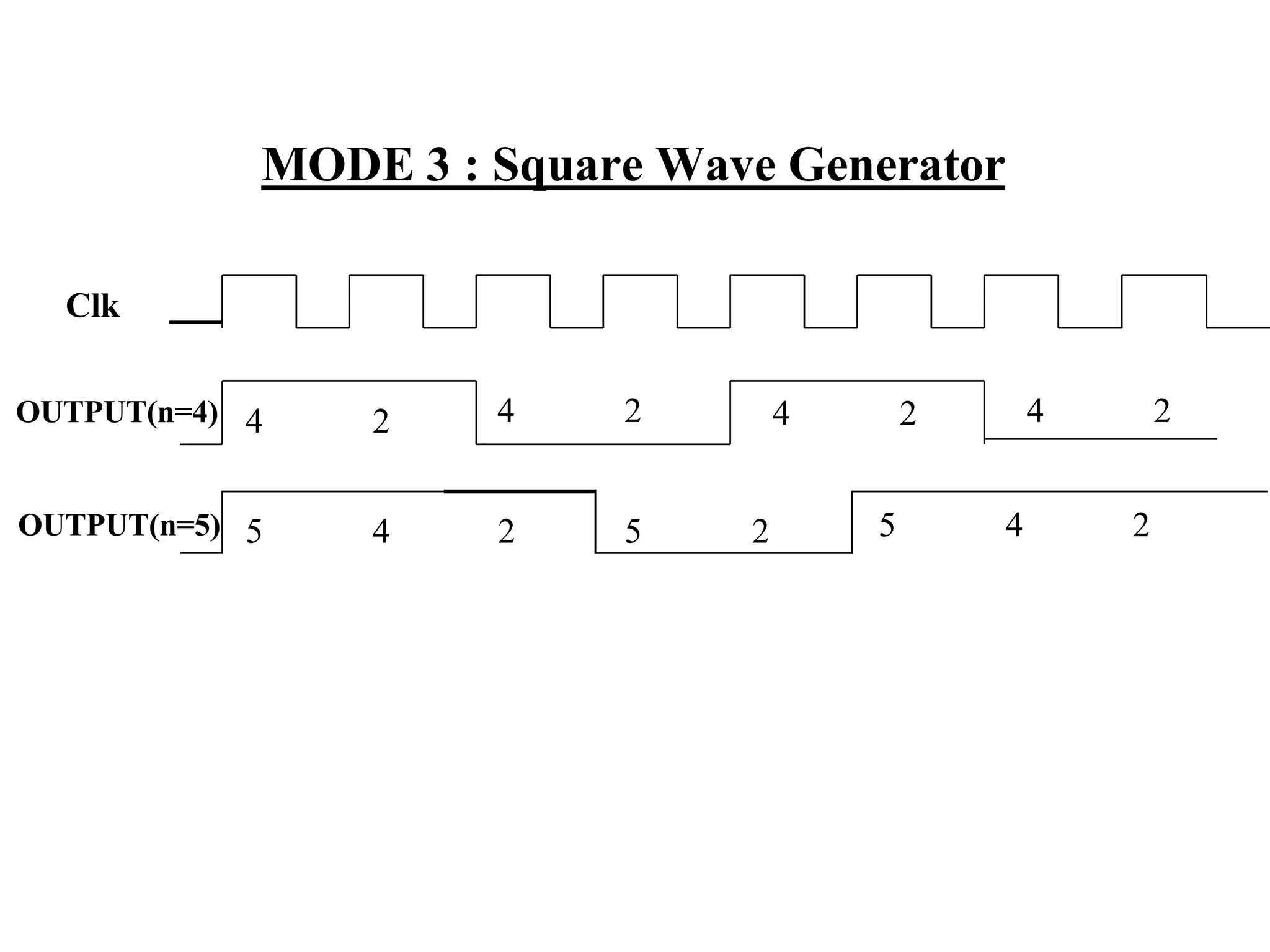
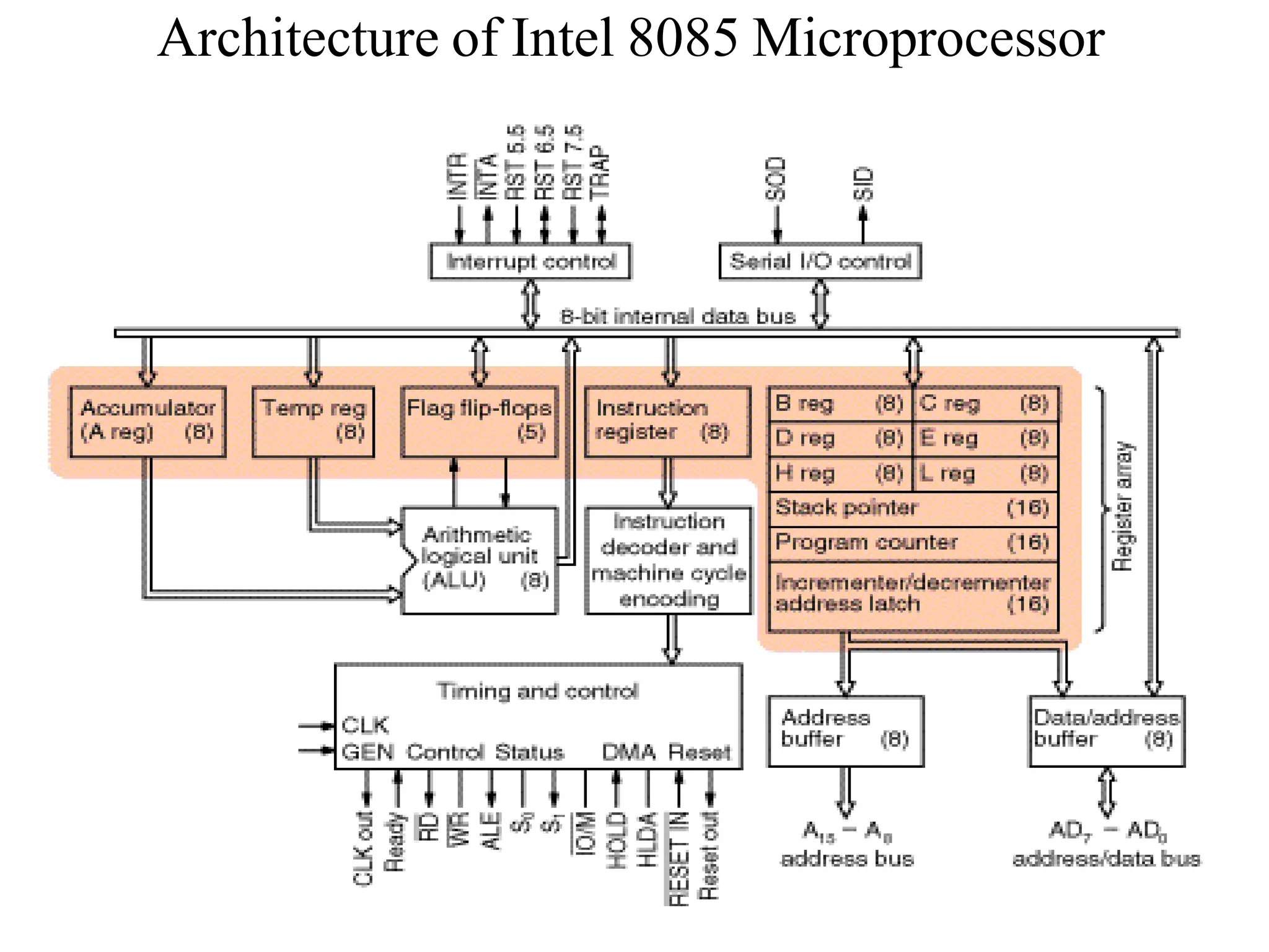
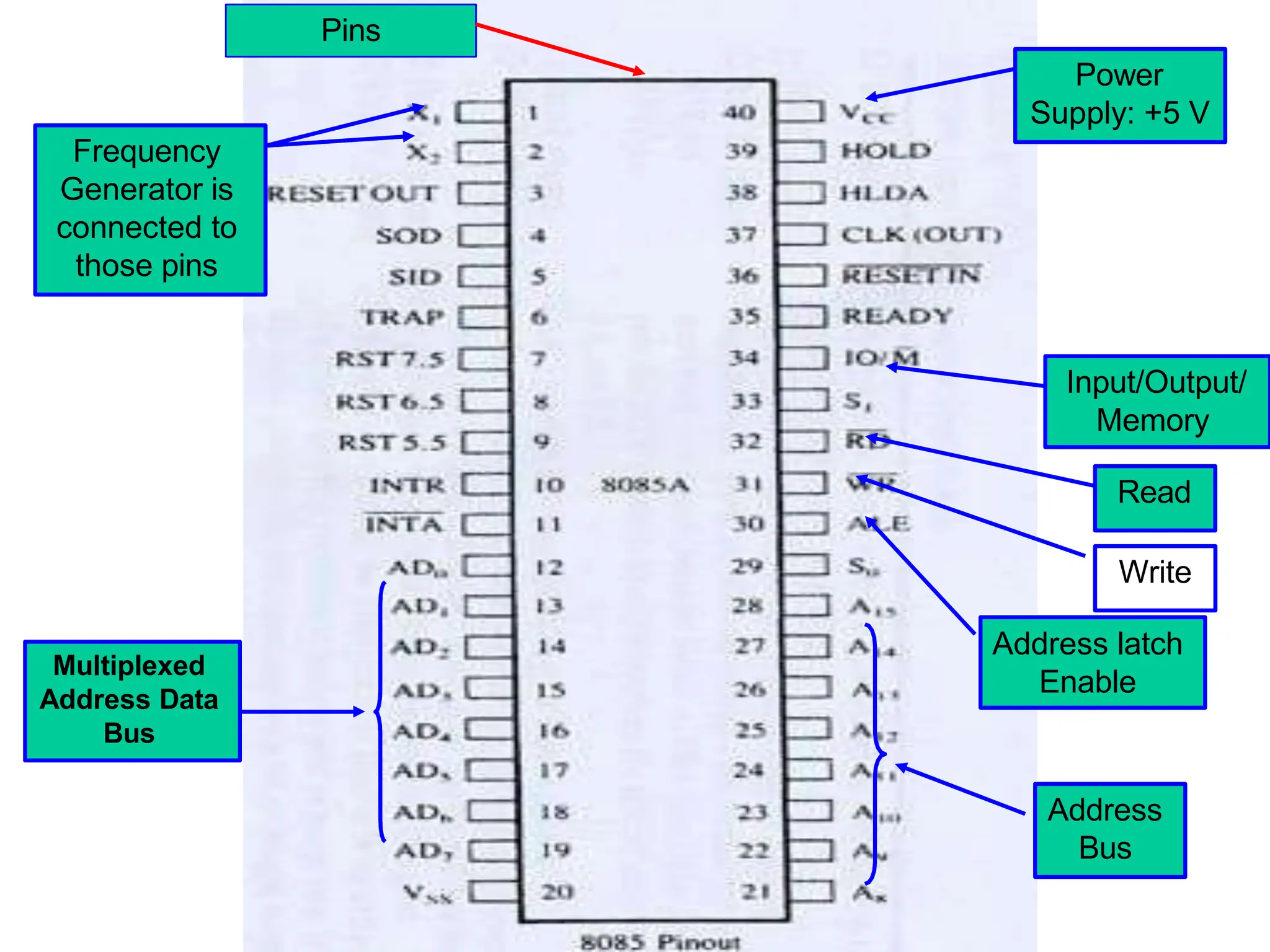
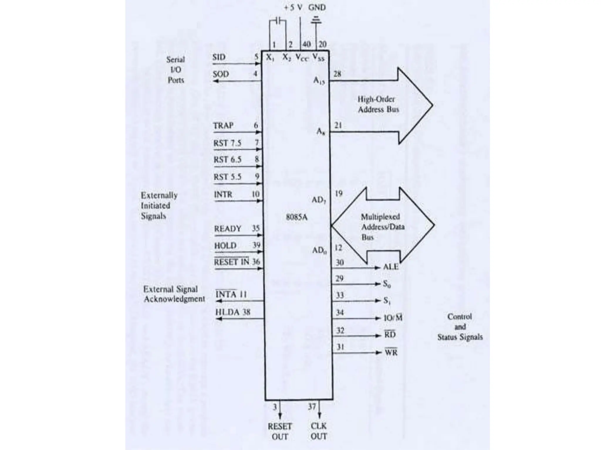
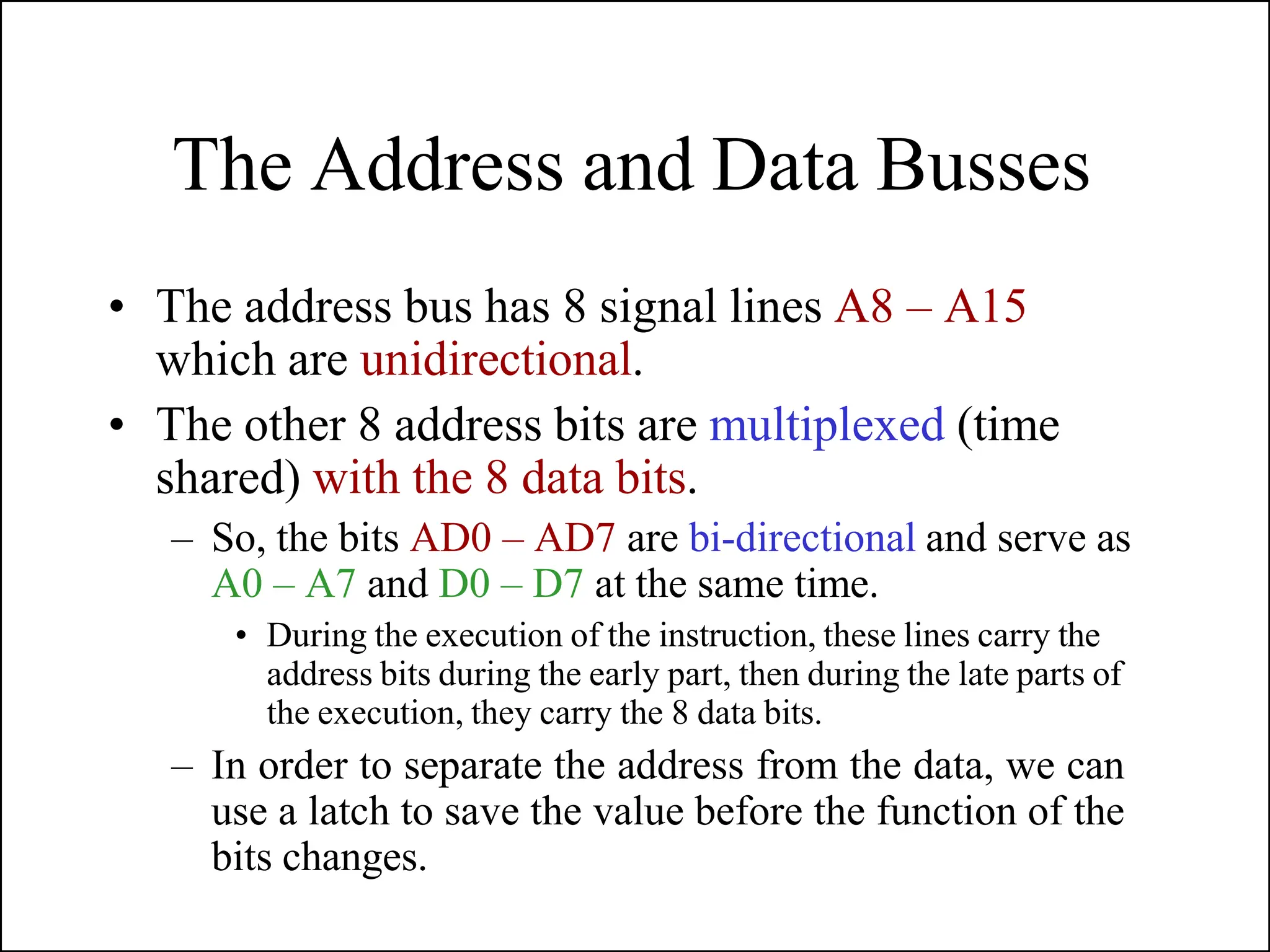
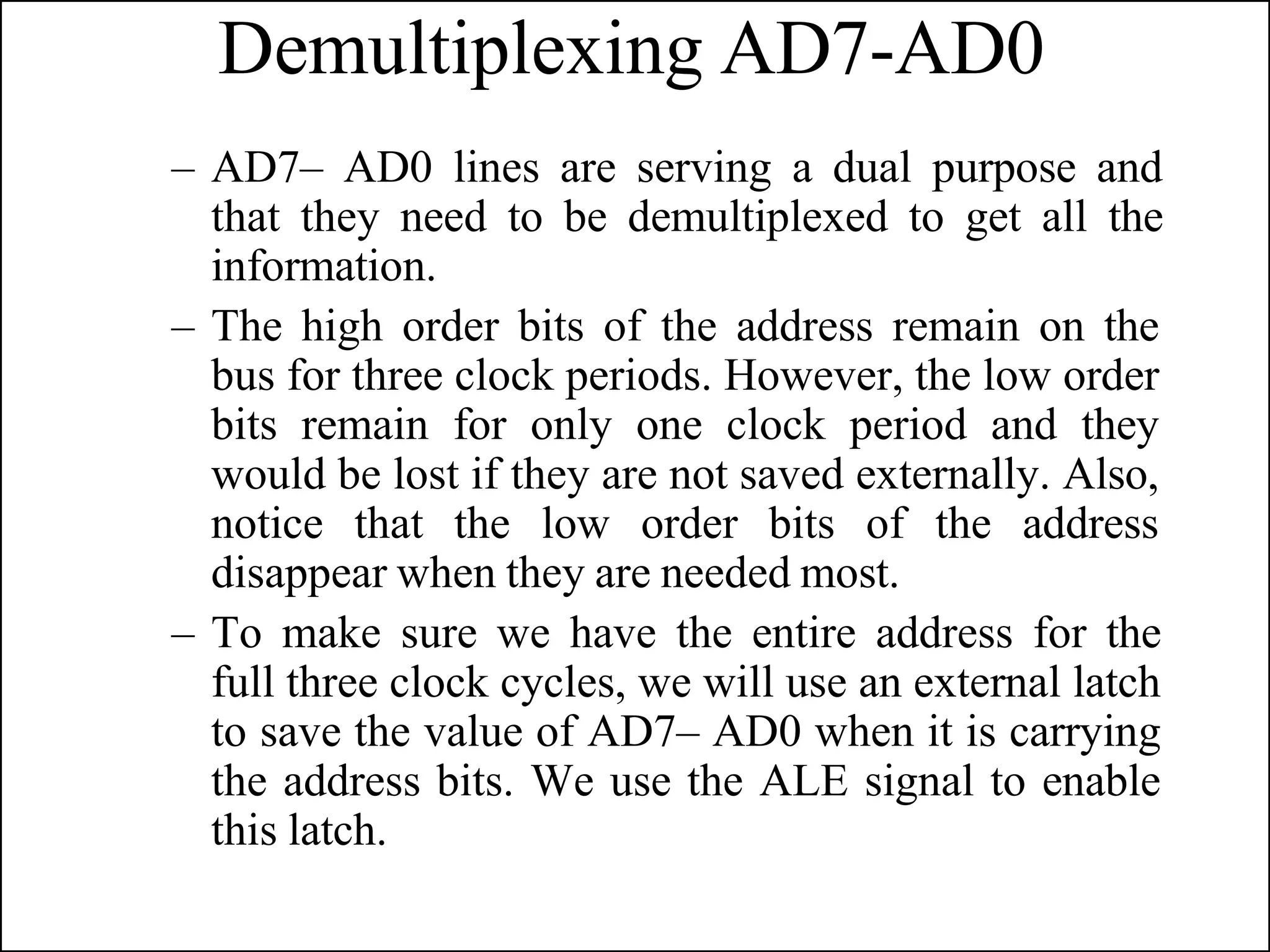
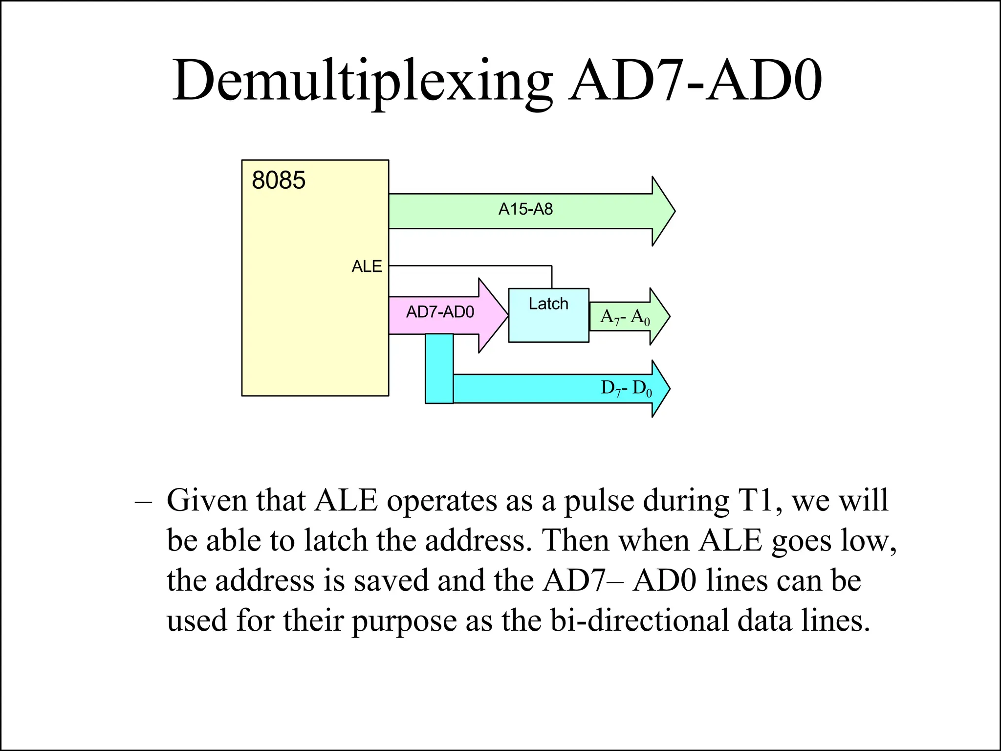
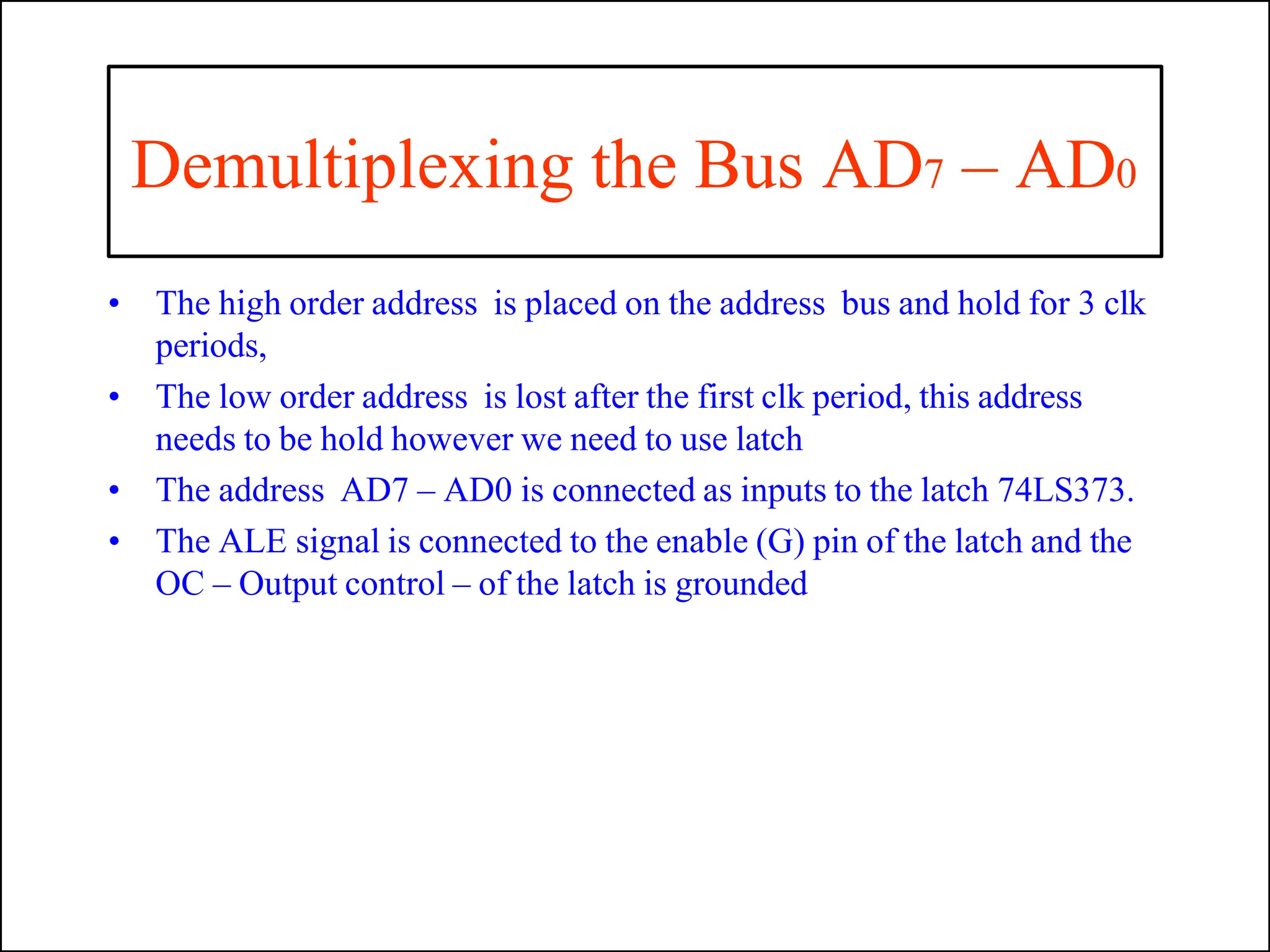
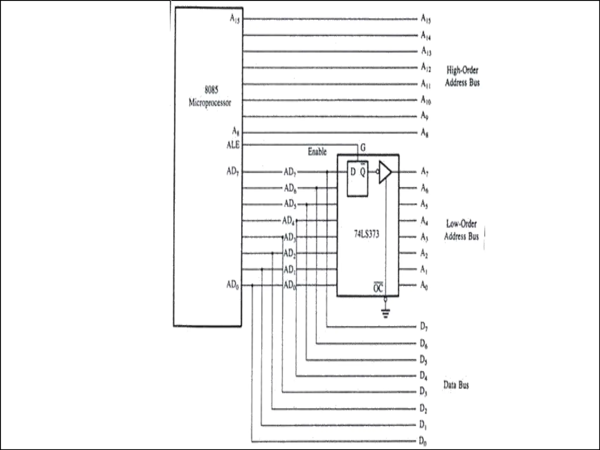
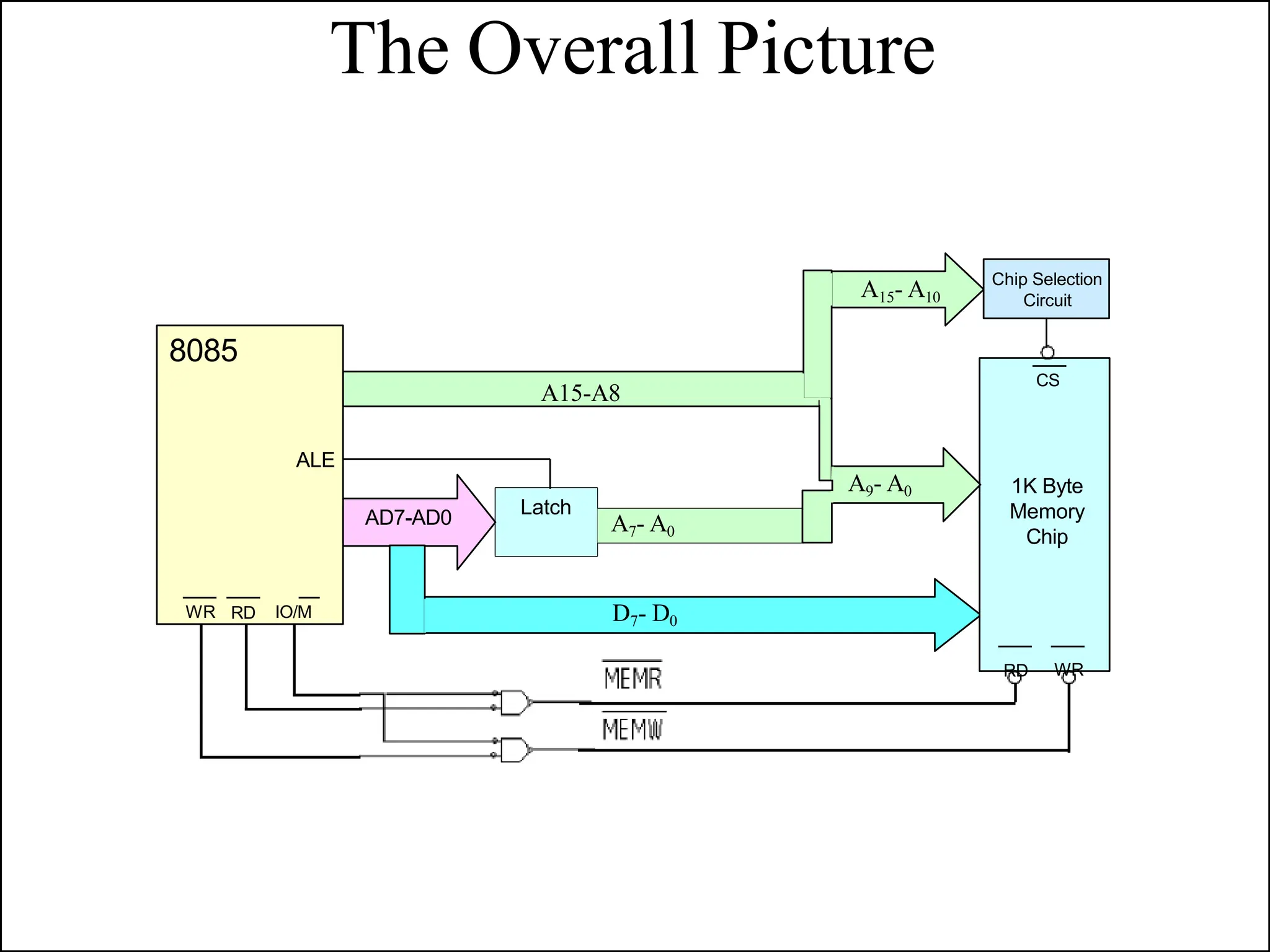
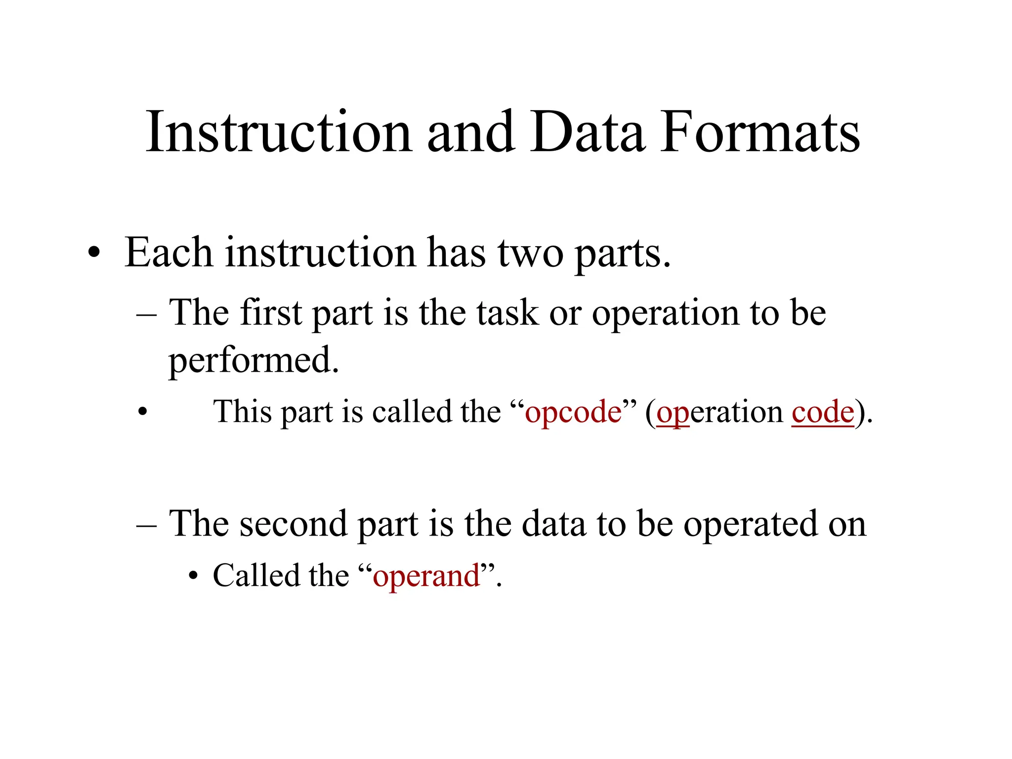
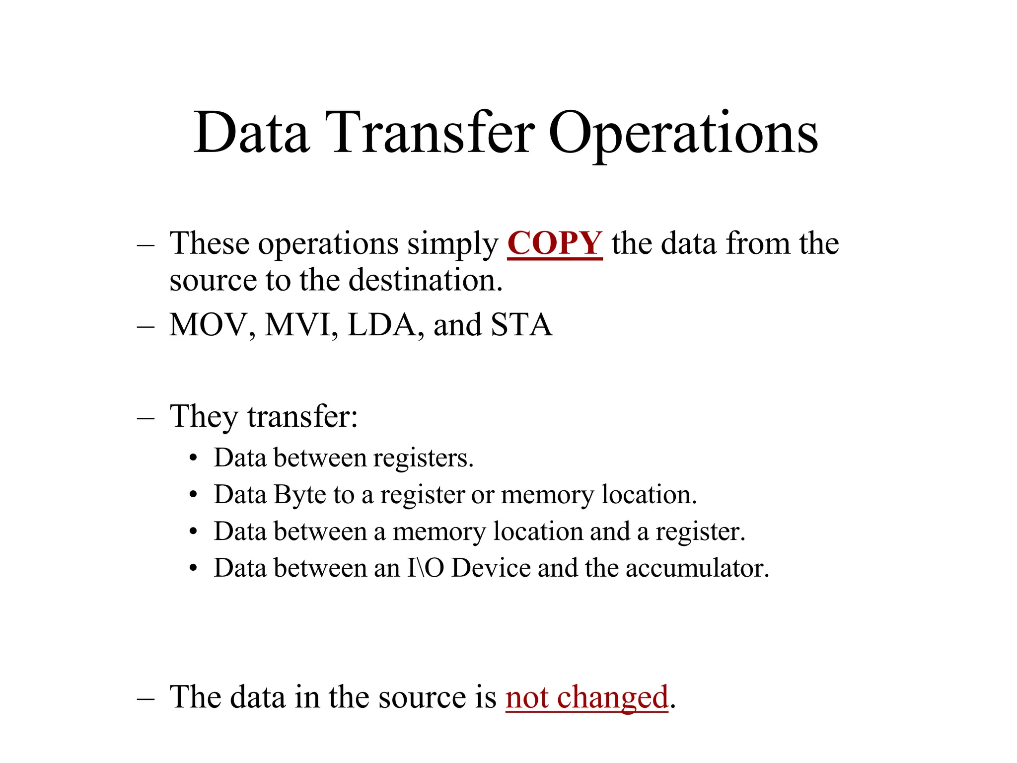
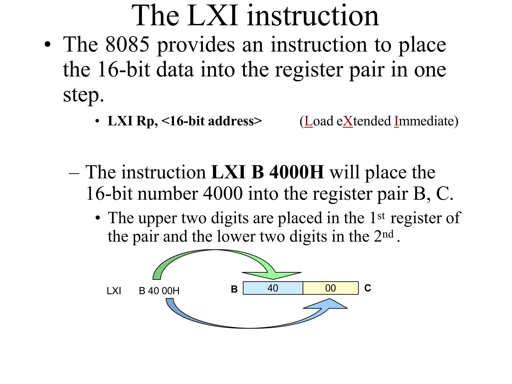
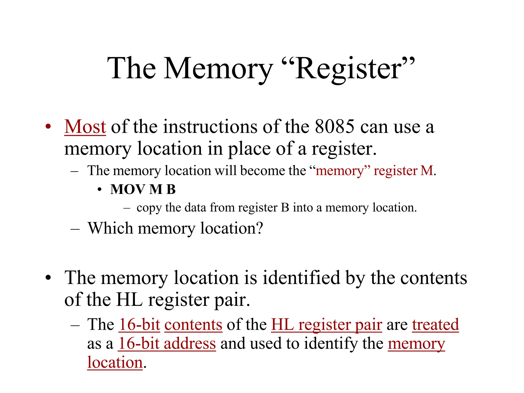
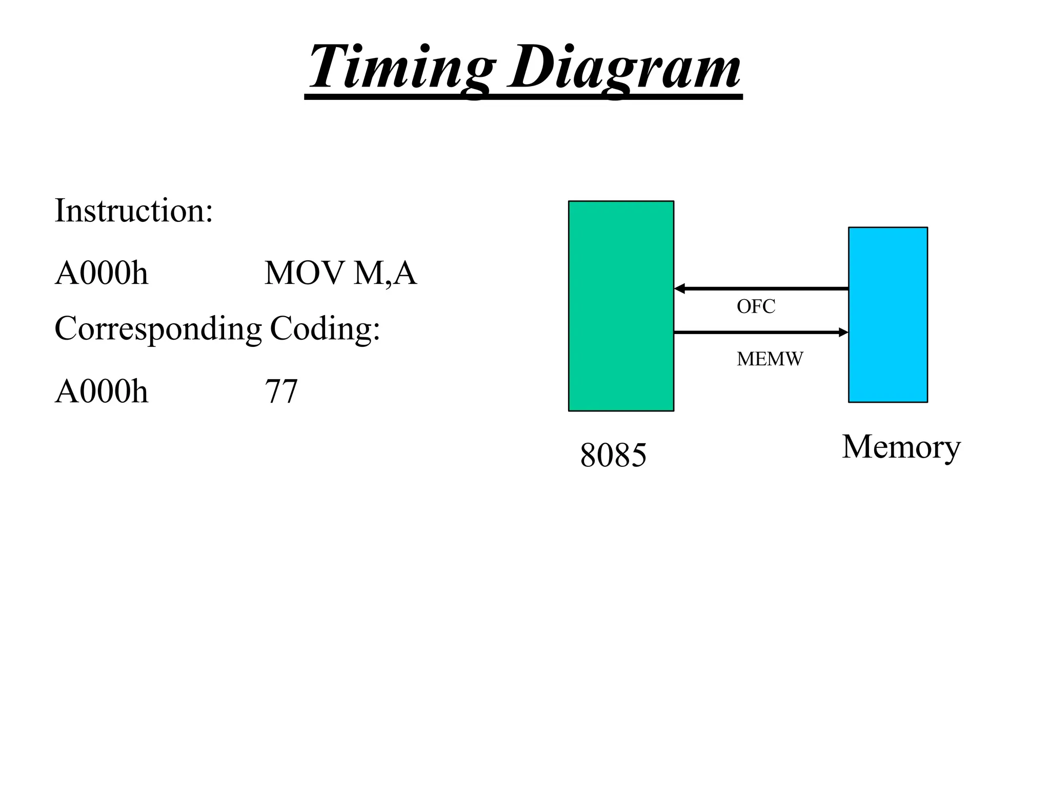
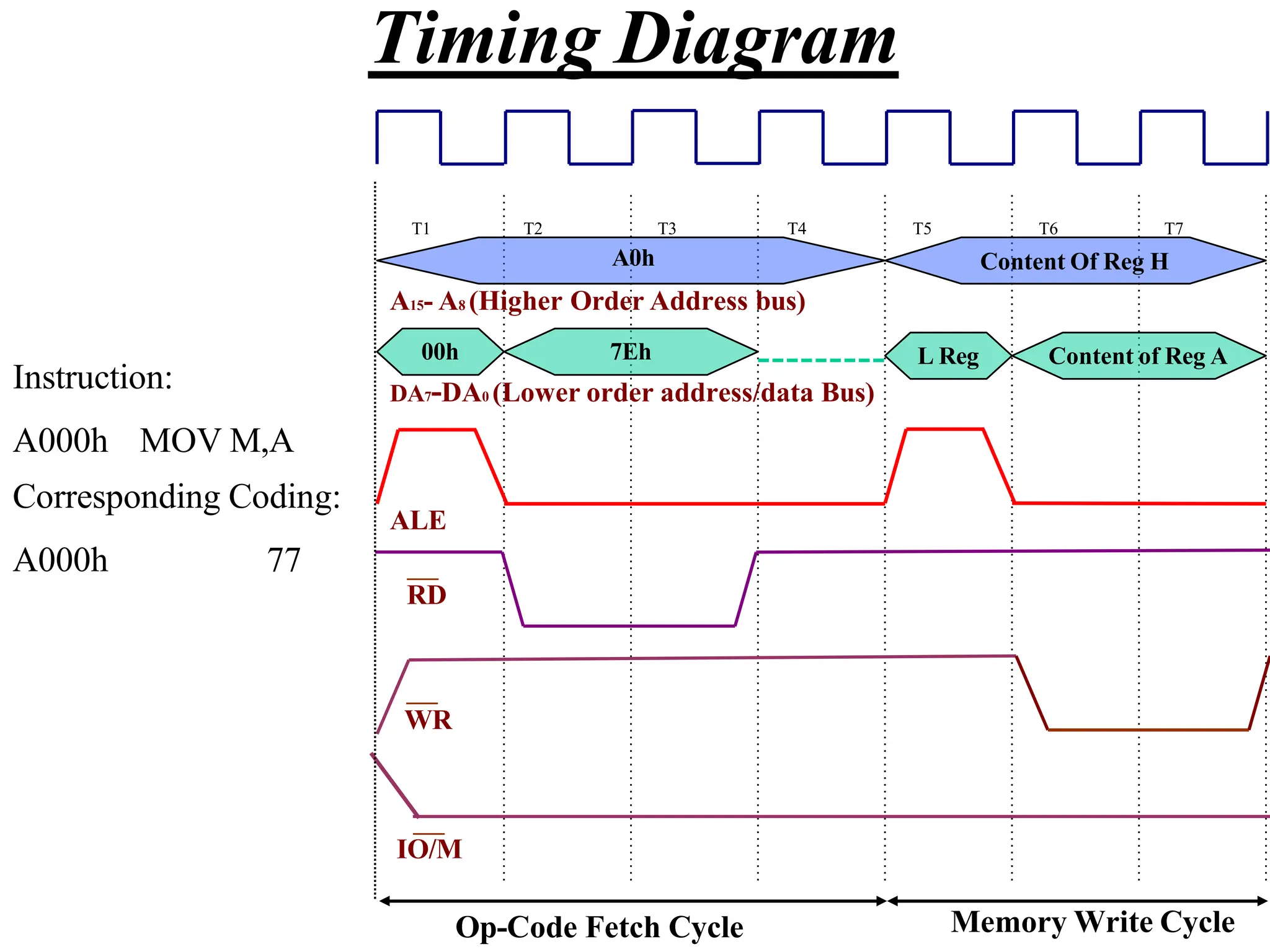
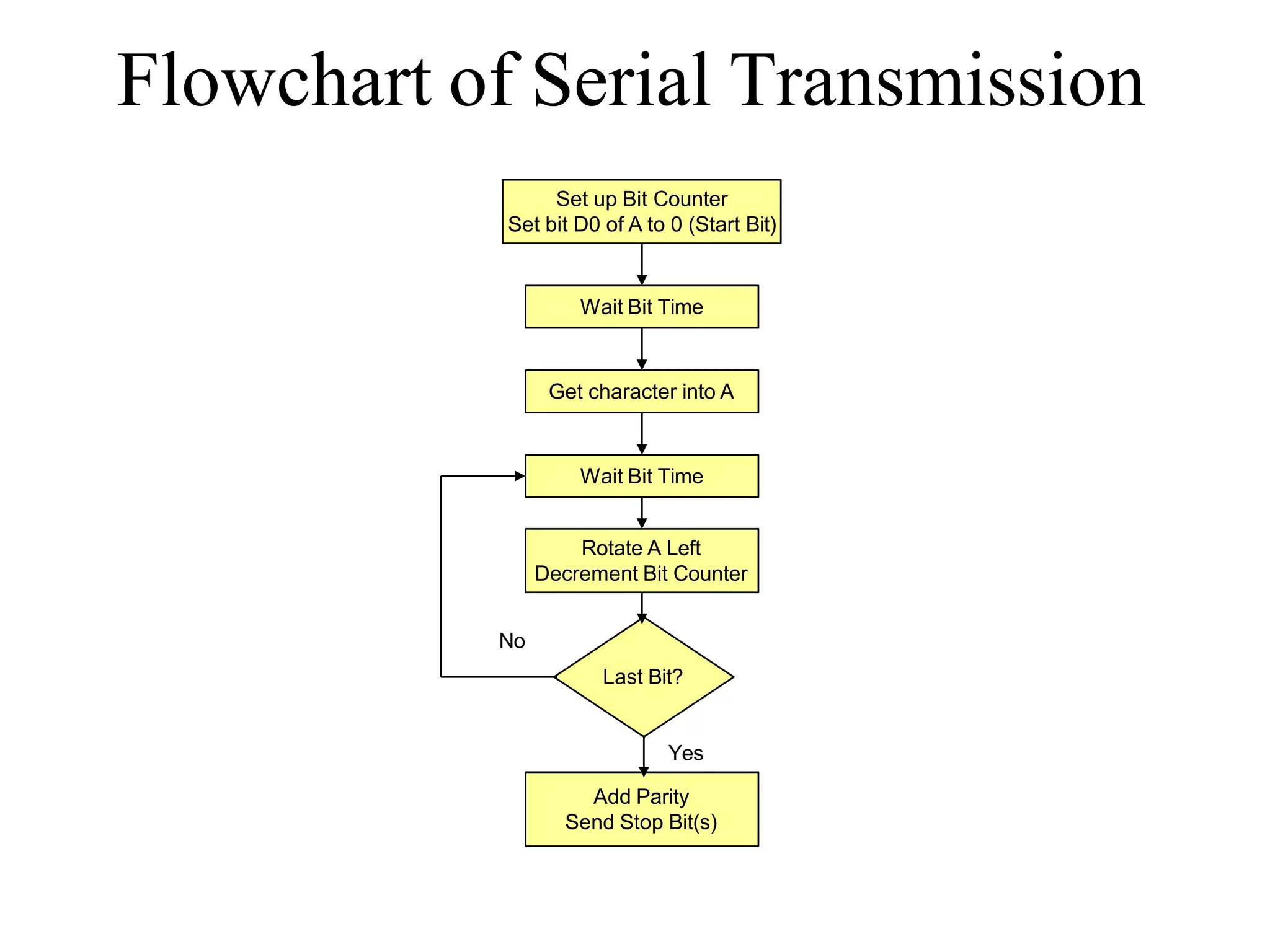
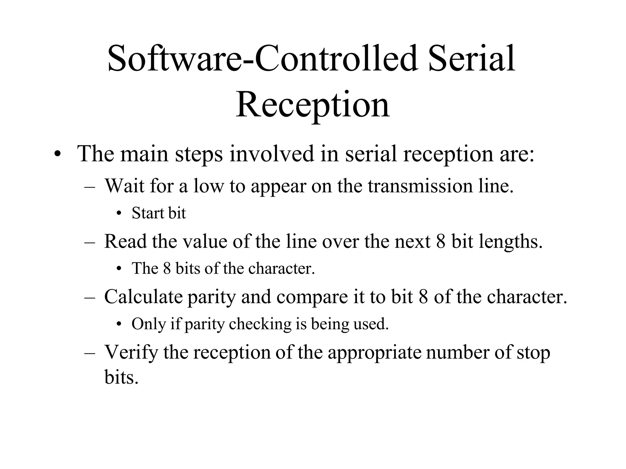
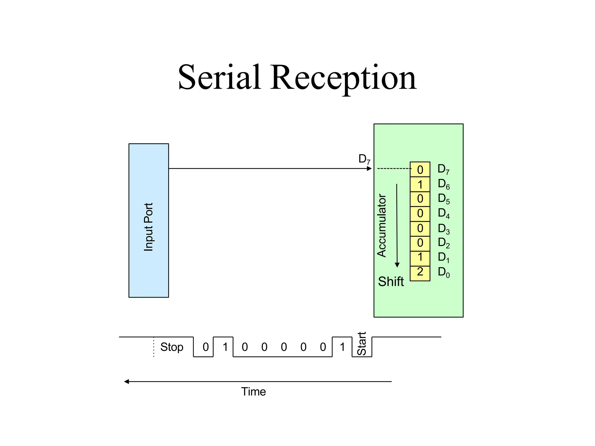
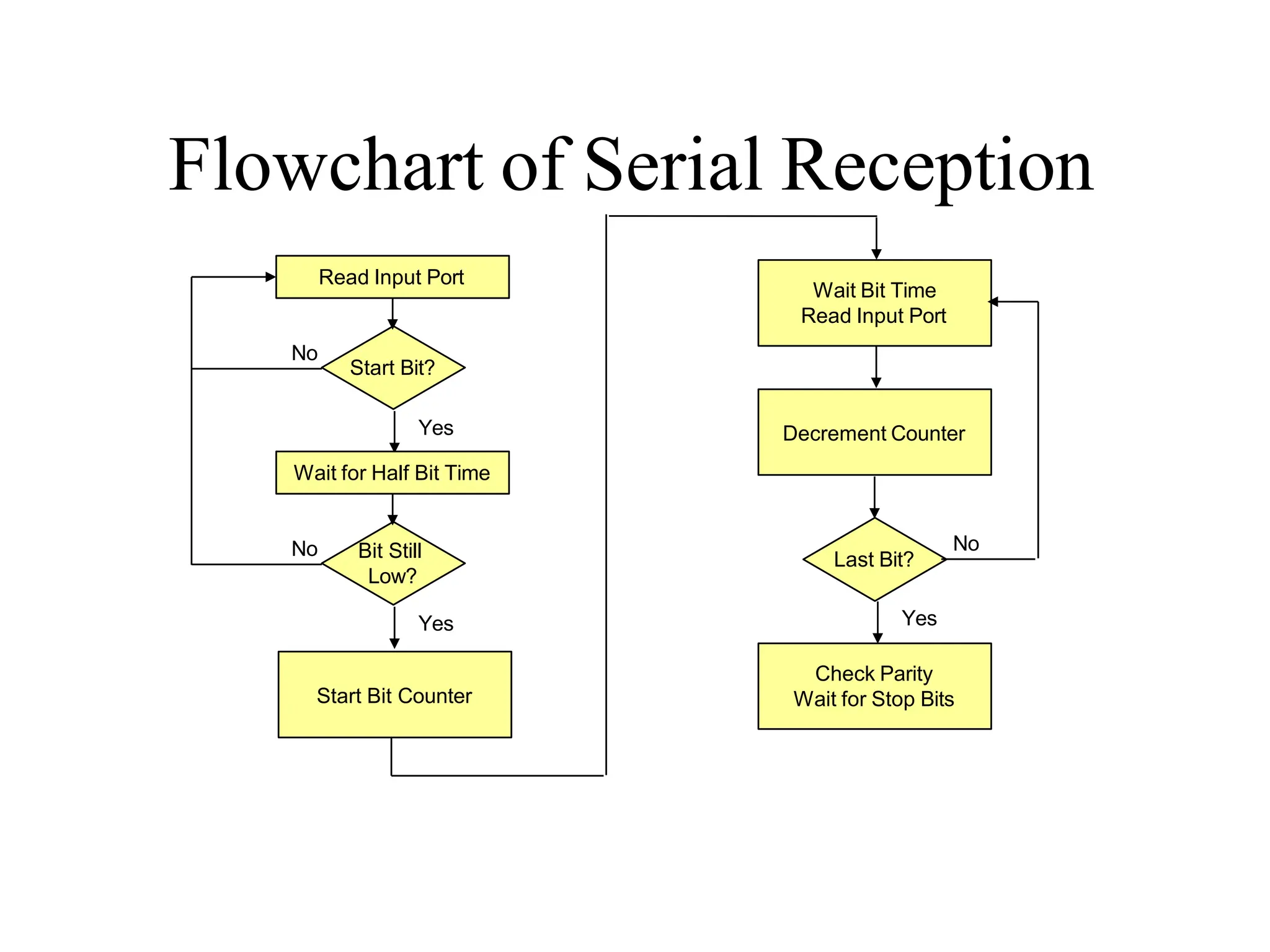
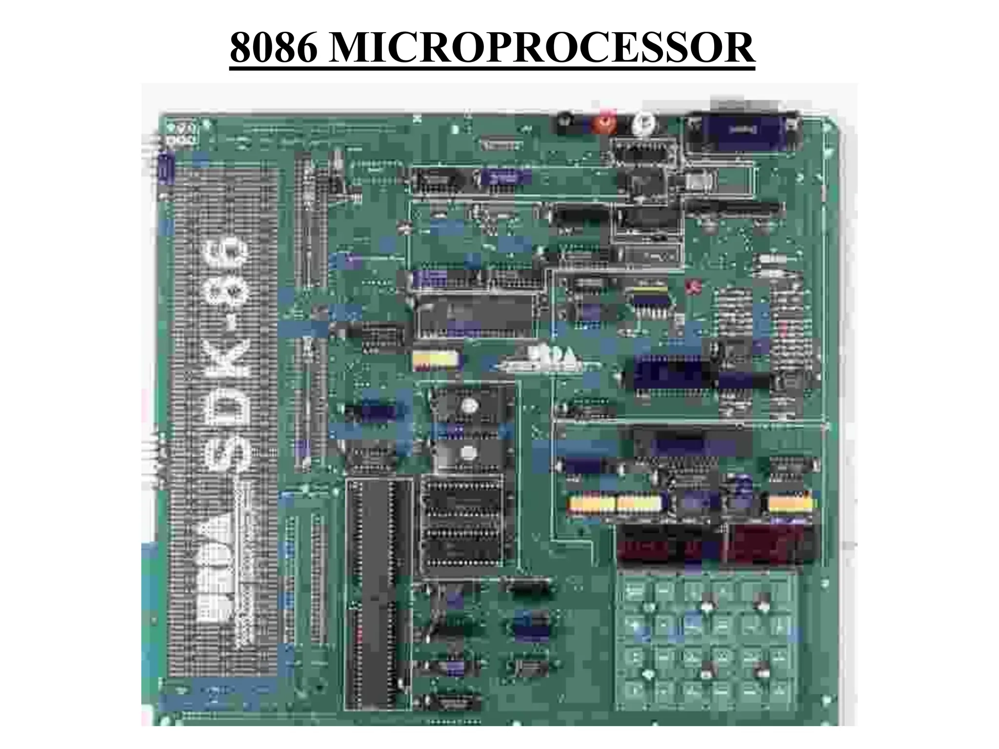
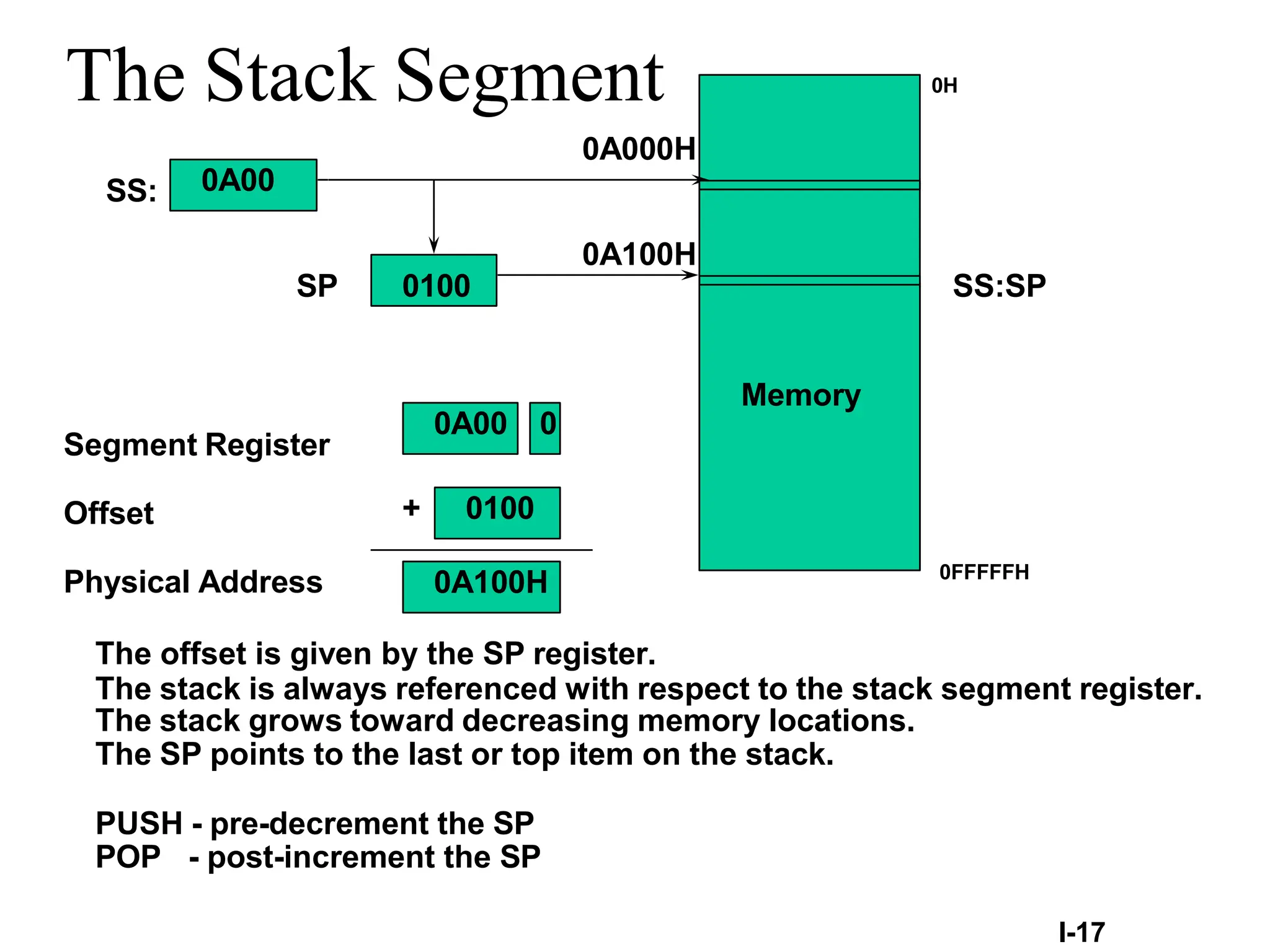
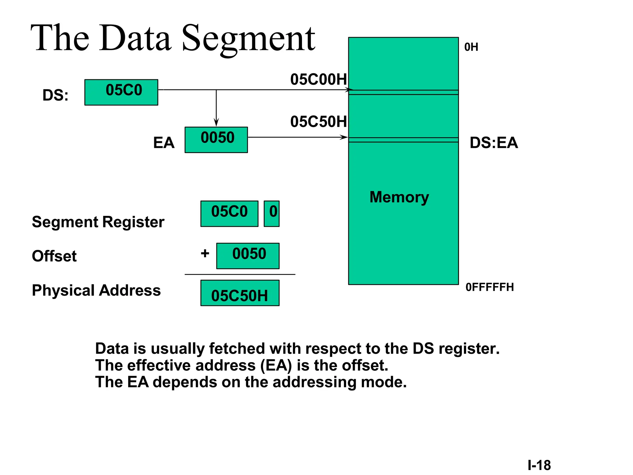
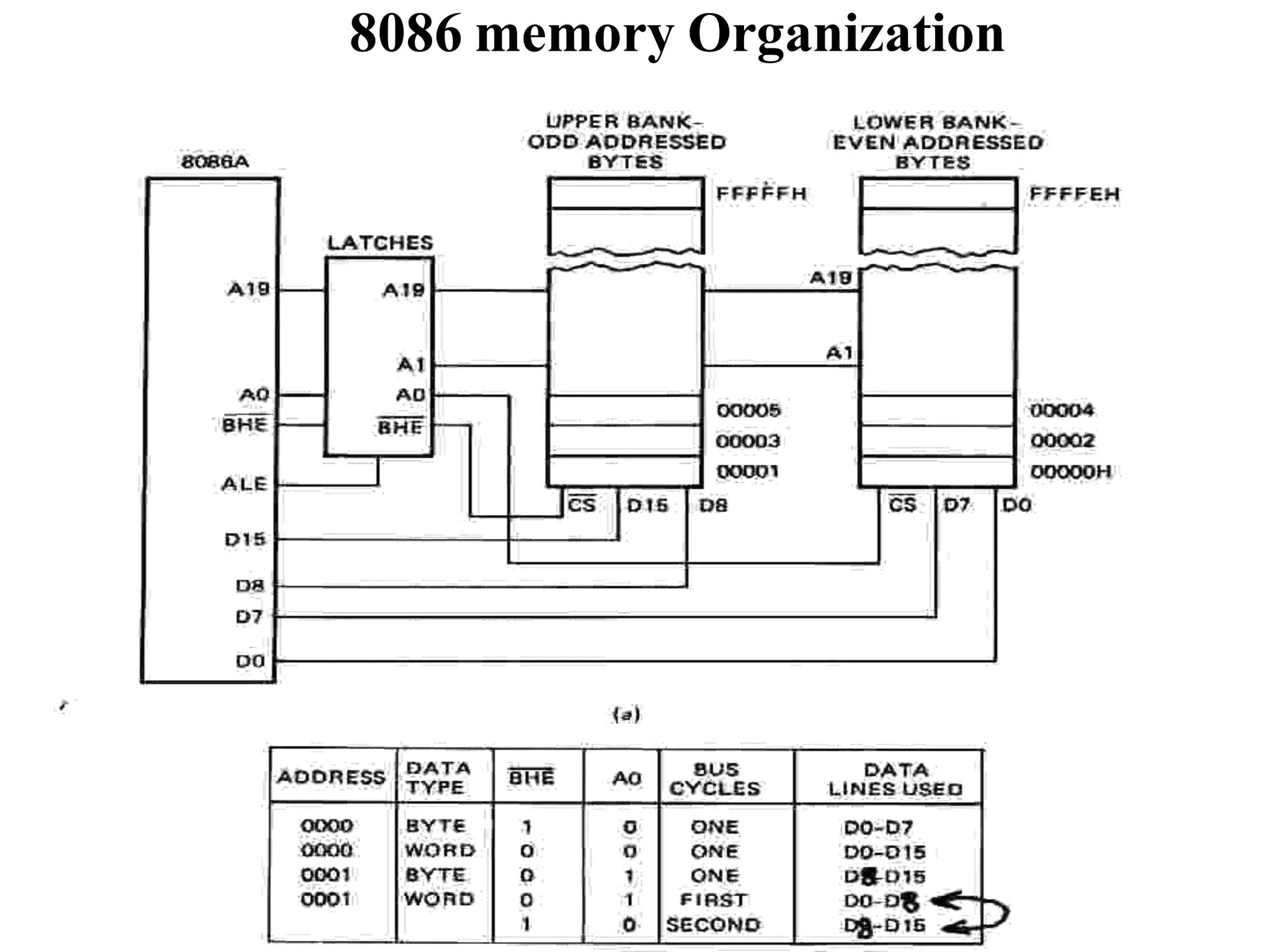
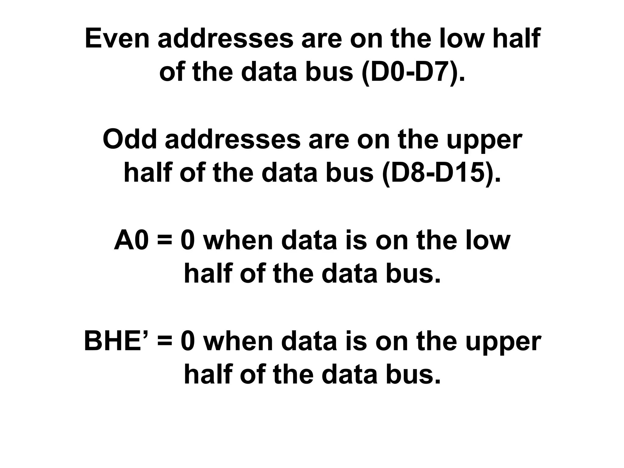
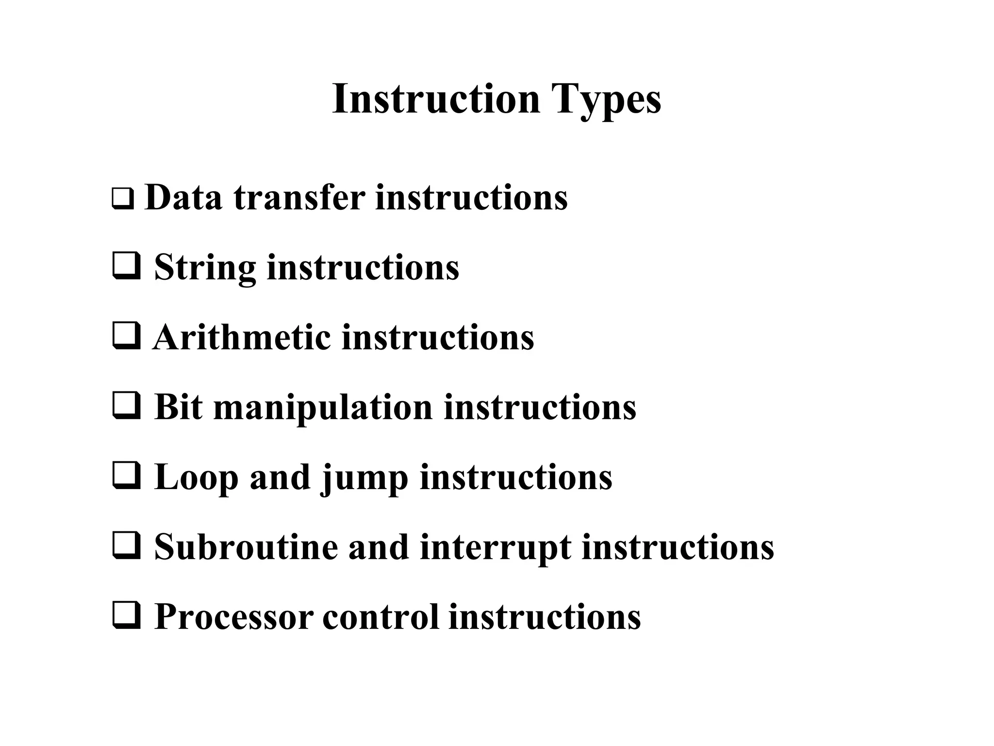
The microprocessor is a programmable device that processes binary numbers according to instructions stored in memory. It contains arithmetic, logic, and control circuits on a single silicon chip. Early processors used discrete components but were large and slow. The invention of the microchip led to much smaller and faster processors by integrating all components onto a single silicon slice. Modern microprocessors manipulate 32-bit or 64-bit words and have instruction sets that define their capabilities. The 8085 was an 8-bit microprocessor that used multiplexed address/data lines, requiring external latching to separate addresses from data.


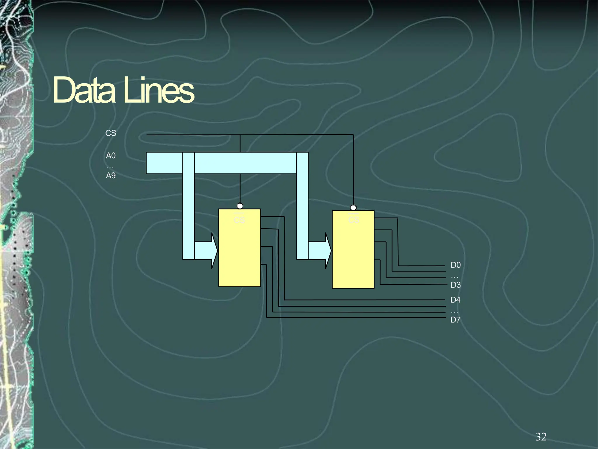
![TheDesignof aMemoryChip
12
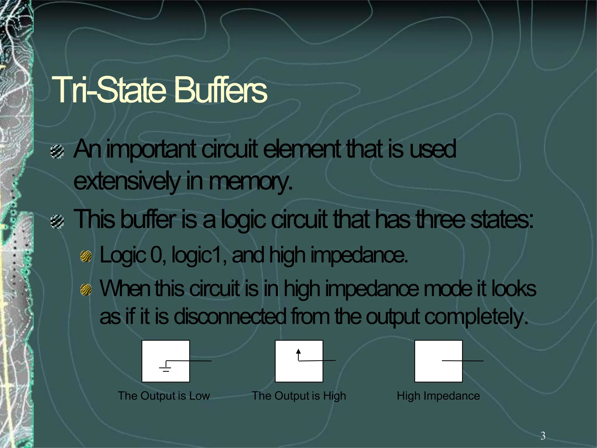
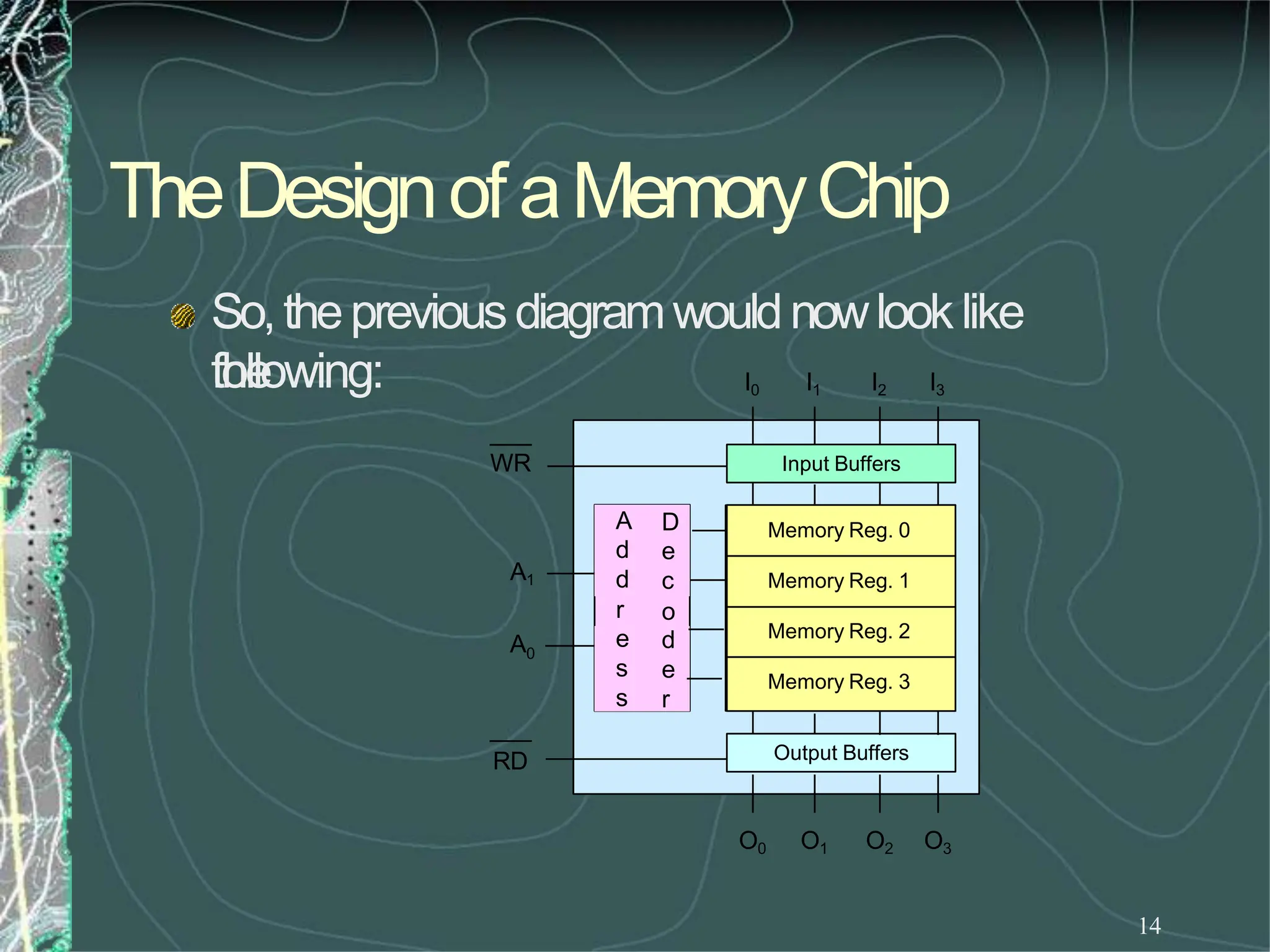
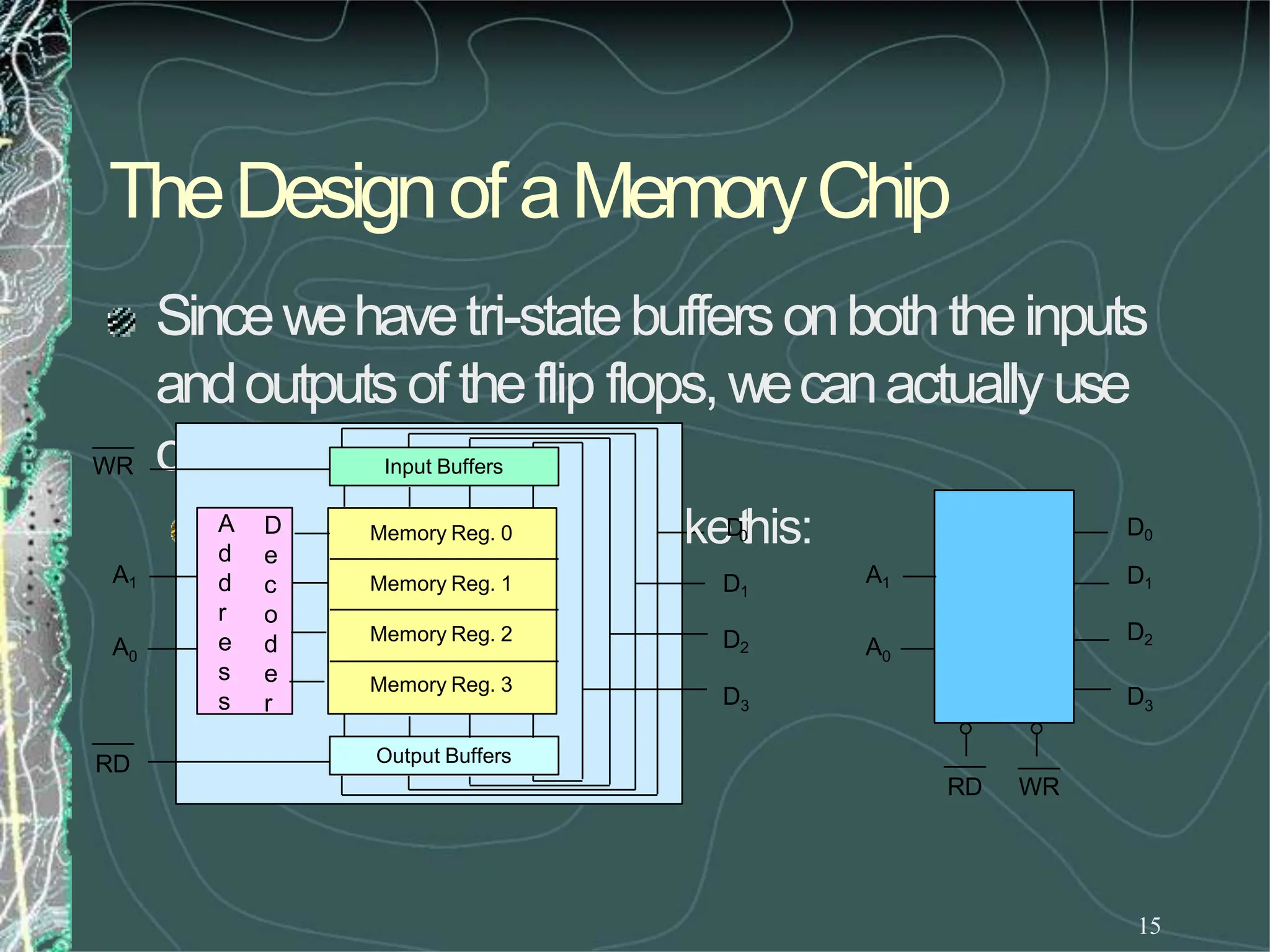
UsingtheRDandWRcontrols wecandeterminethe
direction of flow eitherinto or outof memory.Then
usingtheappropriate Enableinputweenablean
individual memoryregister.
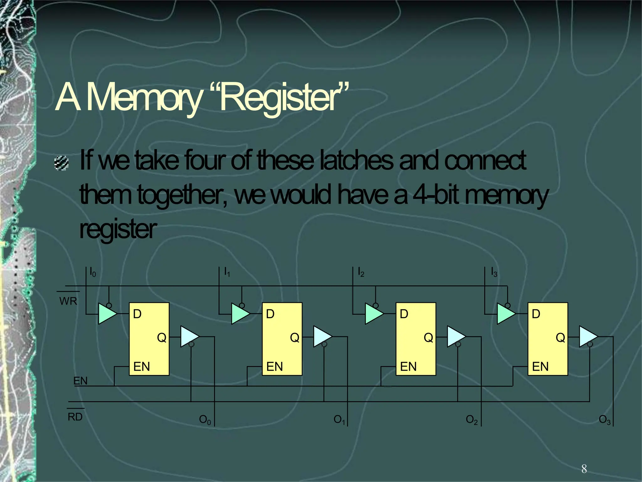
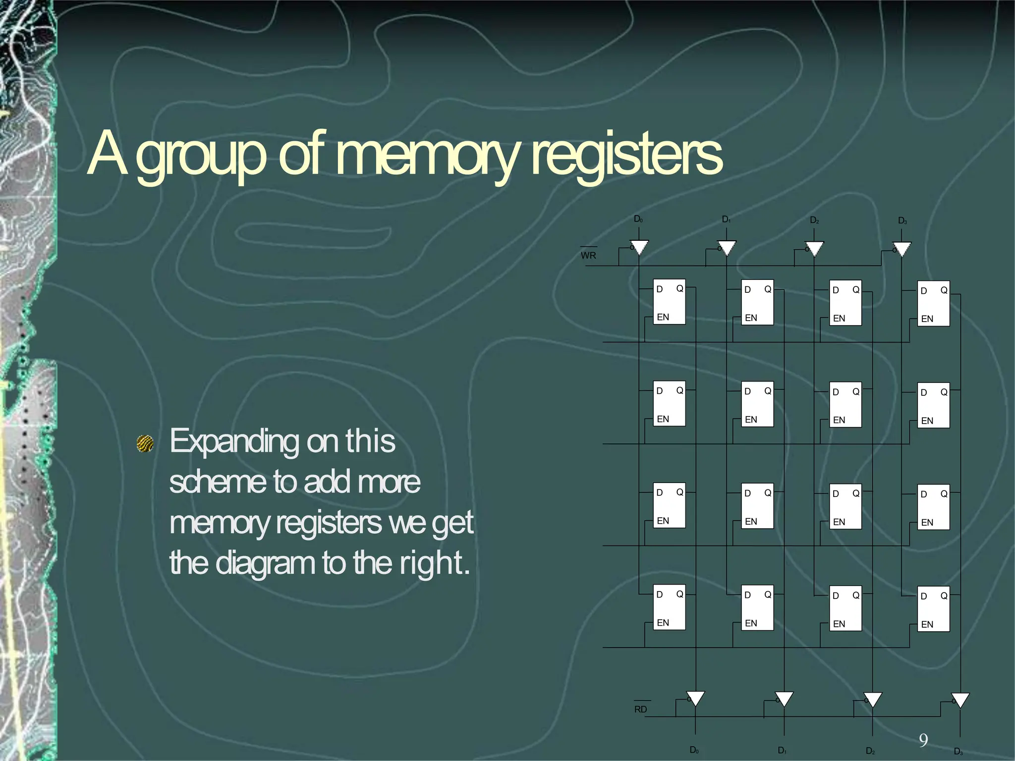
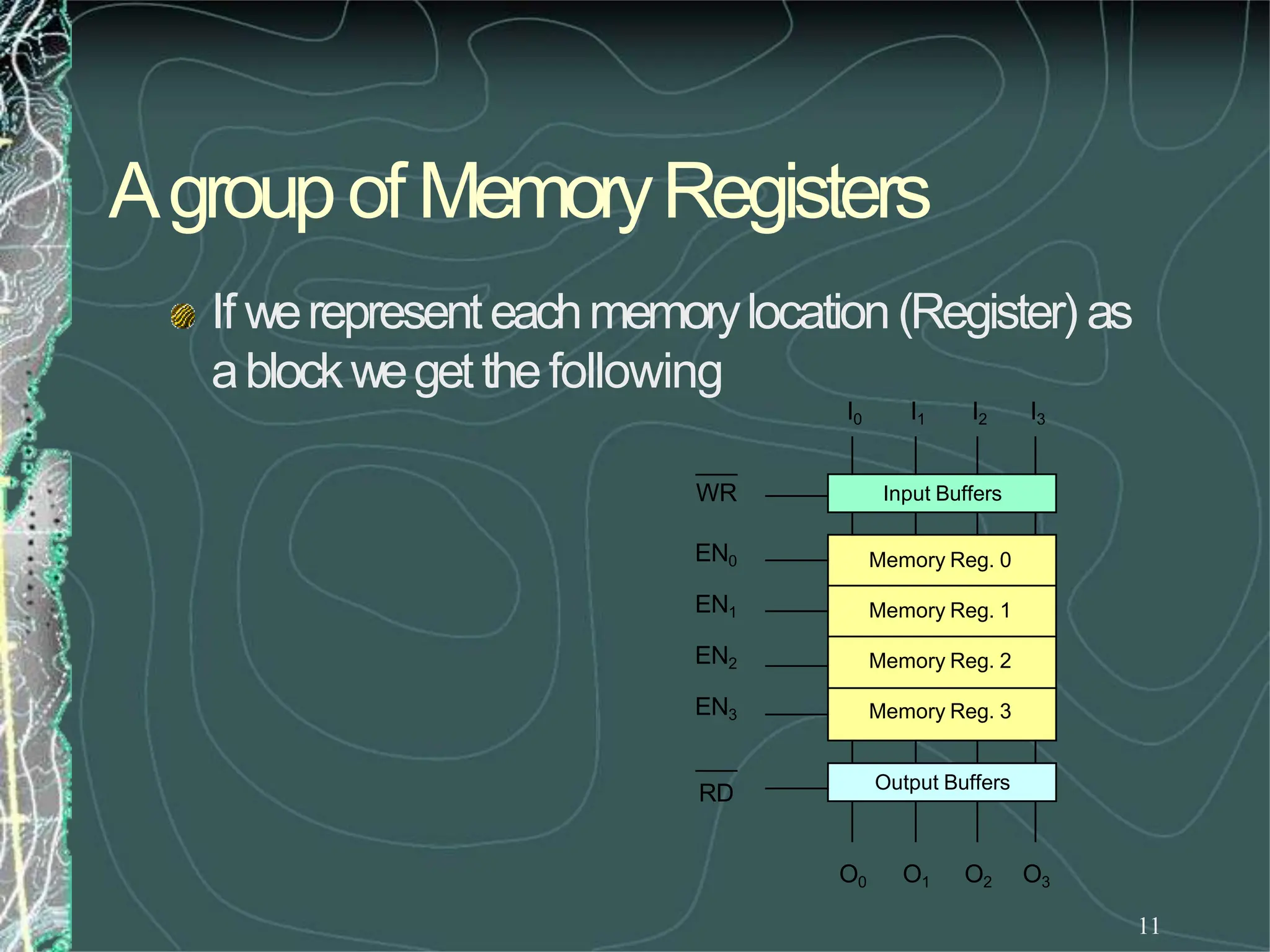
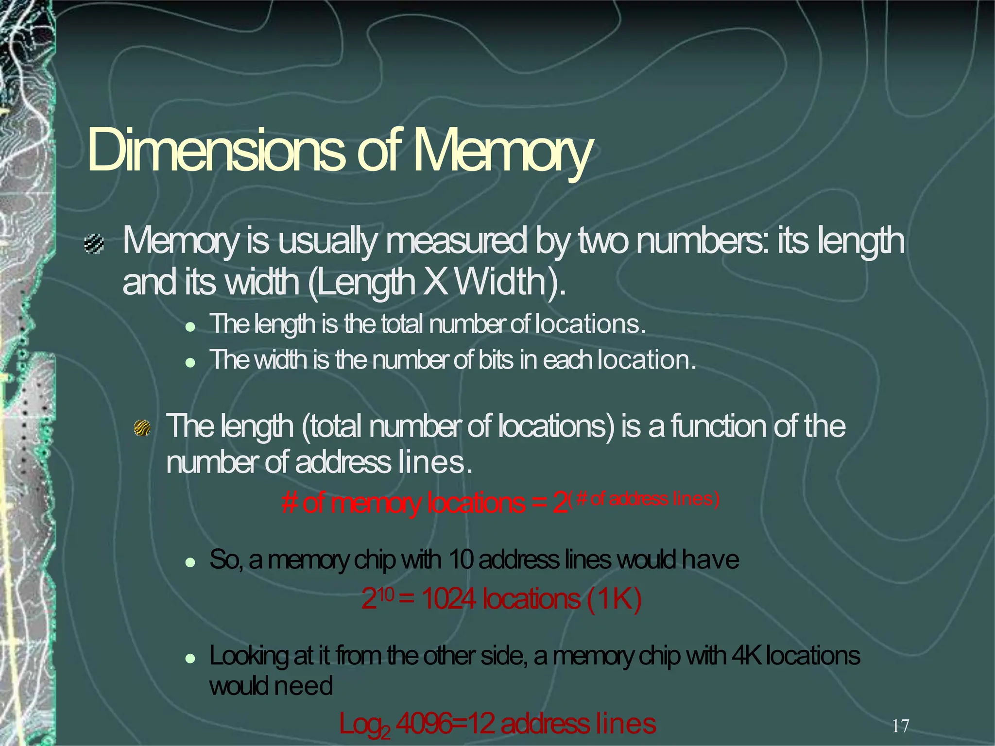
Whatwehavejust designedis amemorywith 4
locations andeachlocationhas4elements (bits). This
memorywouldbecalled4X4[NumberoflocationX
numberof bits per location].](https://image.slidesharecdn.com/8085microprocessor-rameshgaonkar-231105205049-991f4536/75/8085-Microprocessor-Ramesh-Gaonkar-pdf-27-1-pptx-130-2048.jpg)


![Addressing Modes
Immediate addressing
Register addressing
Direct addressing
Register Indirect addressing
Based addressing
Indexed addressing
Based indexed addressing
Based indexed with displacement addressing
MOV AL, 12H
MOV AL, BL
MOV [500H], AL
MOV DL, [SI]
MOV AX, [BX+4]
MOV [DI-8], BL
MOV [BP+SI], AH
MOV CL, [BX+DI+2]
Exceptions
String addressing
Port addressing (e.g. IN AL, 79H)
Addressing Modes Examples](https://image.slidesharecdn.com/8085microprocessor-rameshgaonkar-231105205049-991f4536/75/8085-Microprocessor-Ramesh-Gaonkar-pdf-27-1-pptx-271-2048.jpg)
![Data Transfer Instructions
MOV Destination, Source
— Move data from source to destination; e.g. MOV [DI+100H], AH
— It does not modify flags
For 80x86 family, directly moving data from one memory location to
another memory location is not allowed
MOV [SI], [5000H]
When the size of data is not clear, assembler directives are used
MOV [SI], 0
BYTE PTR
WORD PTR
DWORD PTR
MOV BYTE PTR [SI], 12H
MOV WORD PTR [SI], 12H
MOV DWORD PTR [SI], 12H
You can not move an immediate data to segment register by MOV
MOV DS, 1234H](https://image.slidesharecdn.com/8085microprocessor-rameshgaonkar-231105205049-991f4536/75/8085-Microprocessor-Ramesh-Gaonkar-pdf-27-1-pptx-272-2048.jpg)