The document describes a proposed approach to modify the modified Booth multiplier to generate a more regular partial product array. The conventional MBE generates an irregular array due to an extra partial product bit at the least significant bit position of each row. The proposed approach incorporates this extra bit into the sign extension bits of the first row, reducing the number of rows from n/2+1 to n/2. It generates the partial product bits and new sign extension bits using simple logic gates, minimizing overhead. Experimental results show the proposed MBE multipliers achieve significant improvements in area, delay, and power compared to conventional MBE multipliers due to the more regular array enabling a smaller, faster reduction tree.


![I. INTRODUCTION
ENHANCING the processing performance and reducing the power dissipation of
the systems are the most important design challenges for multimedia and digital signal
processing (DSP) applications, in which multipliers frequently dominate the system’s
performance and power dissipation. Multiplication consists of three major steps: 1) recoding and
generating partial products; 2) reducing the partial products by partial product reduction schemes
(e.g., Wallace tree [1]–[3]) to two rows; and 3) adding the remaining two rows of partial
products by using a carry-propagate adder (e.g., carry look ahead adder) to obtain the final
product. There are already many techniques developed in the past years for these three steps to
improve the performance of multipliers. In this brief, we will focus on the first step (i.e., partial
product generation) to reduce the area, delay, and power consumption of multipliers. The partial
products of multipliers are generally generated by using two-input AND gates or a modified
Booth encoding(MBE) algorithm [3]–[7]. The latter has widely been adopted in parallel
multipliers since it can reduce the number of partial product rows to be added by half, thus
reducing the size and enhancing the speed of the reduction tree. However, as shown in
Fig. 1. Conventional MBE partial product arrays for 8 × 8 multiplication.](https://image.slidesharecdn.com/modifiedbooth-190717135919/85/Modified-booth-7-320.jpg)
![Fig. 1(a), the conventional MBE algorithm generates n/2 + 1partial product rows rather
than n/2 due to the extra partial product bit (neg bit) at the least significant bit position of each
partial product row for negative encoding, leading to an irregular partial product array and a
complex reduction tree. Some approaches [7], [8] have been proposed to generate more regular
partial product arrays, as shown in Fig. 1(b) and (c), for the MBE multipliers. Thus, the area,
delay, and power consumption of the reduction tree, as well as the whole MBE multiplier, can be
reduced. In this brief, we extend the method proposed in [7] to generate a parallelogram-shaped
partial product array, which is more regular than that of [7] and [8]. The proposed approach
reduces the partial product rows from n/2 + 1 to n/2 by incorporating the last neg bit into the sign
extension bits of the first partial product row, and almost no overhead is introduced to the partial
product generator. More regular partial product array and fewer partial product rows result in a
small and fast reduction tree, so that the area, delay, and power of MBE multipliers can further
be reduced. In addition, the proposed approach can also be applied to regularize the partial
product array of post truncated MBE multipliers. Post truncated multiplication, which generates
the 2n-bit product and then rounds the product into n bits, is desirable in many multimedia and
DSP systems due to the fixed register size and bus width inside the hardware.
Experimental results show that the proposed general and post truncated MBE multipliers
with a regular partial product array can achieve significant improvement in area, delay, and
power consumption when compared with conventional MBE multipliers.
TABLE I
MBE TABLE](https://image.slidesharecdn.com/modifiedbooth-190717135919/85/Modified-booth-8-320.jpg)
![1.1. CONVENTIONAL MBEMULTIPLIER
Consider the multiplication of two n-bit integer numbers A (multiplicand) and B (multiplier) in
2’s complement representation,
where b−1 = 0, and mi ∈ {−2,−1, 0, 1, 2}. According to the encoded results from B,
the Booth selectors choose −2A, −A, 0, A, or 2A to generate the partial product rows, as shown in
Table I. The 2A in Table I is obtained by left shifting A one bit. Negation operation is achieved
by complementing each bit of A (one’s complement) and adding “1” to the least significant bit.
Adding “1” is implemented as a correction bit neg, which implies that the partial product row is
negative (neg = 1) or positive (neg = 0). In addition, because partial product rows are represented
in 2’s complement representation and every row is left shifted two bit positions with respect to
the previous row, sign extensions are required to align the most significant parts of partial
product rows. These extra sign bits will significantly complicate the reduction tree. Therefore,
many sign extension schemes [3], [9]–[11] have been proposed to prevent extending up the sign
bit of each row to the (2n − 1)th bit position.
Fig. 1(a) illustrates the MBE partial product array for an 8 × 8 multiplier with a sign
extension prevention procedure, where si is the sign bit of the partial product row PPi, si is the
complement of si, and b_p indicates the bit position. As can beseen in Fig. 1(a), MBE reduces
the number of partial product rows by half, but the correction bits result in an irregular partial
product array and one additional partial product row.](https://image.slidesharecdn.com/modifiedbooth-190717135919/85/Modified-booth-9-320.jpg)
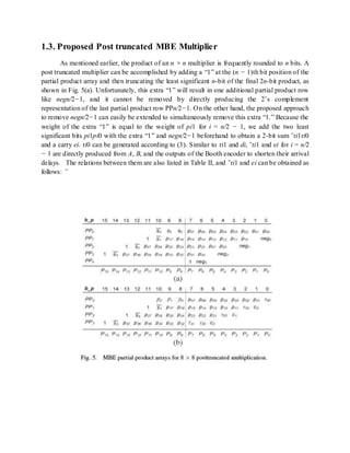
![To have a more regular least significant part of each partial product row PPi, the authors in
[7] added the least significant bit pi0 with negi in advance and obtained a new least significant
bit τi0 Fig. 2. Proposed MBE partial product array for 8 × 8 multiplication. and a carry ci. Note
that both τi0 and ci are generated no later than other partial product bits. Fig. 1(b) depicts the 8 ×
8 MBE partial product array generated by the approach proposed in [7]. Since ci is at the left one
bit position of negi, the required additions in the reduction tree are reduced. However, the
approach does not remove the additional partial product row PP4. The problem is overcome in
[8] by directly producing the 2’s complement representation of the last partial product row
PPn/2−1 while the other partial products are produced so that the last neg bit will not be
necessary.
An efficient method and circuit are developed in [8] to find the 2’s complement of the
last partial product row in a logarithmic time. As shown in Fig. 1(c), the 10-bit last partial
product row and its neg bit in Fig. 1(a) are replaced by the 10-bit 2’s complemented partial
products (s3, s3, t7, t6, . . . , t0) without the last neg bit. Note that one extra “1” is added at the
fourteenth bit position to obtain the correct final product. The approach simplifies and speeds up
the reduction step, particularly for a multiplier that is in the size of a power of 2 and uses 4–2
compressors [12], [13] to achieve modularity and high performance. However, the approach
must additionally develop and design the 2’s complement logic, which possibly enlarges the area
and delay of the partial product generator and lessens the benefit contributed by removing the
extra row.](https://image.slidesharecdn.com/modifiedbooth-190717135919/85/Modified-booth-10-320.jpg)
![1.2.PROPOSED MULTIPLIERS
The proposed MBE multiplier combines the advantages of these two approaches presented in [7]
and [8] to produce a very regular partial product array, as shown in Fig. 2. In the partial product
array, not only each negi is shifted left and replaced by ci but also the last neg bit is removed by
using a simple approach described in detail in the following section. A. Proposed MBE
Multiplier For MB recoding, at least three signals are needed to represent the digit set {−2,−1, 0,
1, 2}. Many different ways have been developed, and Table I shows the encoding scheme
proposed in [14] that is adopted to implement the proposed MBEmultiplier. The Booth encoder
and selector circuits proposed in [14] are depicted in Fig. 3(a) and (b), respectively. Based on the
recoding scheme and the approach proposed in [7], τi0 and ci in Fig. 1(b) can be derived from
the truth table shown in Table II, as follows:
τi0 =onei · a0 = onei + a0------------------------------ (3)
ci =negi · (onei + a0) = negi + onei · a0.------------------------- (4)
Fig. 3. MBE encoder and selector proposed in [14].](https://image.slidesharecdn.com/modifiedbooth-190717135919/85/Modified-booth-11-320.jpg)
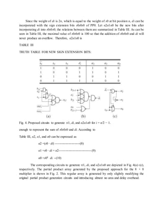
![TABLE II
TRUTH TABLE FOR PARTIAL PRODUCT BITS IN THE PROPOSED PARTIAL
PRODUCT ARRAY:
According to (3) and (4), τi0 and ci can be produced by one NOR gate and one AOI gate,
respectively. Moreover, they are generated no later than other partial product bits. To further
remove the additional partial product row PPn/2 [i.e., PP4 in Fig. 1(b)], we combine the ci for i =
n/2 − 1 with the partial product bit pi1 to produce a new partial product bit τi1 and a new carry
di. Then, the carry di can be incorporated into the sign extension bits of PP0. However, if τi1 and
di are produced by adding ci and pi1, their arrival delays will probably be larger than other
partial product bits. Therefore, we directly produce τi1 and di for i = n/2 − 1 from A, B, and the
outputs of the Booth encoder (i.e., negi, twoi, and onei), as shown in Table II, where L and £
denote the Exclusive-OR and Exclusive-NOR operations, respectively.
The logic expressions of τi1 and di can be written as
τi1 =onei · ε + twoi · a0 = (onei + ε) · (twoi + a0) ---------------------------- (5)
di =(b2i+1 + a0) · [(b2i−1 + a1) · (b2i + a1) · (b2i + b2i−1)]-----------------------(6)
where
ε = La1, if a0 · b2i+1 = 0
a1, otherwise. --------------------(7)](https://image.slidesharecdn.com/modifiedbooth-190717135919/85/Modified-booth-12-320.jpg)
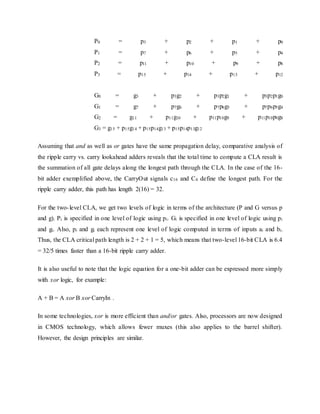
![Figure 3.1. Example of Boolean addition with carry propagation, adapted from [Maf01].
2.2. Boolean Subtraction
When subtracting two numbers, two alternatives present themselves. First, one can
formulate a subtraction algorithm, which is distinct from addition. Second, one can negate the
subtrahend (i.e., in a - b, the subtrahend is b) then perform addition. Since we already know how
to perform addition as well as twos complement negation, the second alternative is more
practical. Figure 2.2 illustrates both processes, using the decimal subtraction 12 - 5 = 7 as an
example.](https://image.slidesharecdn.com/modifiedbooth-190717135919/85/Modified-booth-16-320.jpg)
![Example of Boolean subtraction using (a) unsigned binary representation, and (b) addition
with twos complement negation - adapted from [Maf01].
Just as we have a carry in addition, the subtraction of Boolean numbers uses a borrow. For
example, in Figure 2.2a, in the first (least significant) digit position, the difference 0 - 1 in the
one's place is realized by borrowing a one from the two's place (next more significant digit). The
borrow is propagated upward (toward the most significant digit) until it is zeroed (i.e., until we
encounter a difference of 1 - 0).
2.3. Overflow
Overflow occurs when there are insufficient bits in a binary number representation to portray the
result of an arithmetic operation. Overflow occurs because computer arithmetic is not closed
with respect to addition, subtraction, multiplication, or division. Overflow cannot occur in
addition (subtraction), if the operands have different (resp. identical) signs.
To detect and compensate for overflow, one needs n+1 bits if an n-bit number representation is
employed. For example, in 32-bit arithmetic, 33 bits are required to detect or compensate for
overflow. This can be implemented in addition (subtraction) by letting a carry (borrow) occur
into (from) the sign bit. To make a pictorial example of convenient size, Figure 3.3 illustrates the](https://image.slidesharecdn.com/modifiedbooth-190717135919/85/Modified-booth-17-320.jpg)
![four possible sign combinations of differencing 7 and 6 using a number representation that is
four bits long (i.e., can represent integers in the interval [-8,7]).
Example of overflow in Boolean arithmetic, adapted from [Maf01].
2.4. MIPS Overflow Handling
MIPS raises an exception when overflow occurs. Exceptions (or interrupts) act like procedure
calls. The register $epc stores the address of the instruction that caused the interrupt, and the
instruction
mfc register, $epc
moves the contents of $epc to register. For example, register could be $t1. This is an efficient
approach, since no conditional branch is needed to test for overflow.
Two's complement arithmetic operations (add, addi, and sub instructions) raise exceptions on
overflow. In contrast, unsigned arithmetic (addu and addiu) instructions do not raise an
exception on overflow, since they are used for arithmetic operations on addresses (recall our
discussion of pointer arithmetic in Section 2.6). In terms of high-level languages, C ignores
overflows (always uses addu, addiu, and subu), while FORTRAN uses the appropriate](https://image.slidesharecdn.com/modifiedbooth-190717135919/85/Modified-booth-18-320.jpg)
![instruction to detect overflow. Figure 3.4 illustrates the use of conditional branch on overflow for
signed and unsigned addition operations.
Example of overflow in Boolean arithmetic, adapted from [Maf01].
2.5. Logical Operations
Logical operations apply to fields of bits within a 32-bit word, such as bytes or bit fields (in C, as
discussed in the next paragraph). These operations include shift-left and shift-right operations
(sll and srl), as well as bitwise and, or (and, andi, or, ori). As we saw in Section 2, bitwise
operations treat an operand as a vector of bits and operate on each bit position.
C bit fields are used, for example, in programming communications hardware, where
manipulation of a bit stream is required. In Figure 3.5 is presented C code for an example
communications routine, where a structure called receiver is formed from an 8-bit field called
receivedByte and two one-bit fields called ready and enable. The C routine sets receiver.ready
to 0 and receiver.enable to 1.](https://image.slidesharecdn.com/modifiedbooth-190717135919/85/Modified-booth-19-320.jpg)
![Figure 2.5. Example of C bit field use in MIPS, adapted from [Maf01].
Note how the MIPS code implements the functionality of the C code, where the state of the
registers $s0 and $s1 is illustrated in the five lines of diagrammed register contents below the
code. In particular, the initial register state is shown in the first two lines. The sll instruction
loads the contents of $s1 (the receiver) into $s0 (the data register), and the result of this is shown
on the second line of the register contents. Next, the srl instruction left-shifts $s0 24 bits,
thereby discarding the enable and ready field information, leaving just the received byte. To
signal the receiver that the data transfer is completed, the andi and ori instructions are used to
set the enable and ready bits in $s1, which corresponds to the receiver. The data in $s0 has
already been received and put in a register, so there is no need for its further manipulation.](https://image.slidesharecdn.com/modifiedbooth-190717135919/85/Modified-booth-20-320.jpg)
![Figure 3.6. Example of a simple 1-bit ALU, where the oval represents a multiplexer with a
control code denoted by Op and an output denoted by C - adapted from [Maf01].
3.3. Full Adder. Now let us consider the one-bit adder. Recalling the carry situation shown in
Figure 3.1, we show in Figure 3.7 that there are two types of carries - carry in (occurs at the
input) and carry out (at the output).
Figure 3.7. Carry-in and carry-out in Boolean addition, adapted from [Maf01].
Here, each bit of addition has three input bits (Ai, Bi, and CarryIni), as well as two output bits
(Sumi, CarryOuti), where CarryIni+1 = CarryOuti. (Note: The "i" subscript denotes the i-th bit.)
This relationship can be seen when considering the full adder's truth table, shown below:](https://image.slidesharecdn.com/modifiedbooth-190717135919/85/Modified-booth-22-320.jpg)
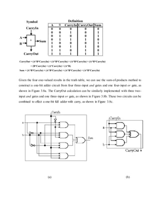
![(c)
Figure 3.7. Full adder circuit (a) sum-of-products form from above-listed truth table, (b)
CarryOut production, and (c) one-bit full adder with carry - adapted from [Maf01].
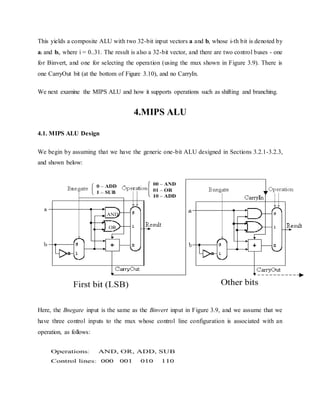
Recalling the symbol for the one-bit adder, we can add an addition operation to the one-bit ALU
shown in Figure 3.6. This is done by putting two control lines on the output mux, and by having
an additional control line that inverts the b input (shown as "Binvert") in Figure 3.9).](https://image.slidesharecdn.com/modifiedbooth-190717135919/85/Modified-booth-24-320.jpg)
![(a) (b)
Figure 3.9. One-bit ALU with three operations: and, or, and addition: (a) Least significant bit,
(b) Remaining bits - adapted from [Maf01].
3.4. 32-bit ALU Design
The final implementation of the preceding technique is in a 32-bit ALU that incorporates the
and, or, and addition operations. The 32-bit ALU can be simply constructed from the one-bit
ALU by chaining the carry bits, such that CarryIni+1 = CarryOuti, as shown in Figure 3.10.
Figure 3.10. 32-bit ALU with three operations: and, or, and addition - adapted from [Maf01].](https://image.slidesharecdn.com/modifiedbooth-190717135919/85/Modified-booth-25-320.jpg)
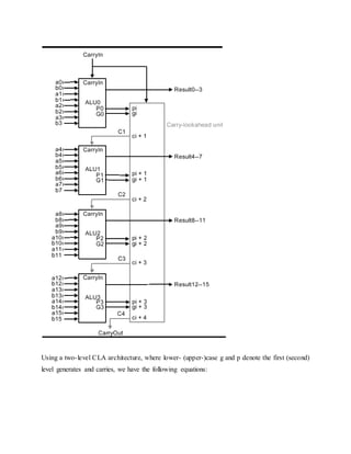
![Figure 3.11. One-bit ALU with additional logic for slt operation - adapted from [Maf01].
Thus, for a 32-bit ALU, the additional cost of the slt instruction is (a) augmentation of each of
32 muxes to have three control lines instead of two, (b) augmentation of each of 32 one-bit
ALU's control signal structure to have an additional (Less) input, and (c) the addition of overflow
detection circuitry, a Set output, and an xor gate on the output of the sign bit.
4.2. Support for the bne Instruction. Recall the branch-on-not-equal instruction bne r1, r2,
Label, where r1 and r2 denote registers and Label is a branch target label or address. To
implement bne, we observe that the following implication holds:
A - B = 0 => A = B .
then add hardware to test if the comparison between A and B implemented as (A - B) is zero.
Again, this can be done using negation and the full adder that we have already designed as part
of the ALU. The additional step is to or all 32 results from each of the one-bit ALUs, then invert](https://image.slidesharecdn.com/modifiedbooth-190717135919/85/Modified-booth-28-320.jpg)
![the output of the or operation. Thus, if all 32 bits from the one-bit full adders are zero, then the
output of the or gate will be zero (inverted, it will be one). Otherwise, the output of the or gate
wil be one (inverted, it will be zero). We also need to consider A - B, to see if there is overflow
when A = 0. A block diagram of the hardware modification is shown in Figure 3.12.
Figure 3.12. 32-bit ALU with additional logic to support bne and slt instructions - adapted from
[Maf01].
Here, the additional hardware involves 32 separate output lines from the 342 one-bit adders, as
well as a cascade of or gates to implement a 32-input nor gate (which doesn't exist in practice,
due to excessive fan-in requirement).
4.3. Support for Shift Instructions. Considering the sll, srl, and sra instructions, these are
supported in the ALU under design by adding a data line for the shifter (both left and right).](https://image.slidesharecdn.com/modifiedbooth-190717135919/85/Modified-booth-29-320.jpg)
![However, the shifters are much more easily implemented at the transistor level (e.g., outside the
ALU) rather than trying to fit more circuitry onto the ALU itself.
In order to implement a shifter external to the ALU, we consider the design of a barrel shifter,
shown schematically in Figure 3.13. Here, the closed siwtch pattern, denoted by black filled
circles, is controlled by the CPU through control lines to a mux or decoder. This allows data line
xi to be sent to output xj, where i and j can be unequal.
Figure 3.13. Four bit barrel shifter, where "x >> 1" denotes a shift amount greater than one -
adapted from [Maf01].
This type of N-bit shifter is well understood and easy to construct, but has space complexity of
O(N2).
4.4. Support for Immediate Instructions. In the MIPS immediate instruction formats, the first
input to the ALU is the first register (we'll call it rs) in the immediate command, while the
second input is either data from a register rt or a zero or sign-extended constant (immediate). To
support this type of instruction, we need to add a mux at the second input of the ALU, as shown
in Figure 3.14. This allows us to select whether rt or the sign-extended immediate is input to the
ALU.](https://image.slidesharecdn.com/modifiedbooth-190717135919/85/Modified-booth-30-320.jpg)
![Figure 3.14. Supporting immediate instructions on a MIPS ALU design, where IR denotes the
instruction register, and (/16) denotes a 16-bit parallel bus - adapted from [Maf01].
4.5 ALU Performance Issues
When estimating or measuring ALU performance, one wonders if a 32-bit ALU is as fast as a 1-
bit ALU - what is the degree of parallelism, and do all operations execute in parallel? In practice,
some operations on N-bit operands (e.g., addition with sequential propagation of carries) take
O(N) time. Other operations, such as bitwise logical operations, take O(1) time. Since addition
can be implemented in a variety of ways, each with a certain level of parallelism, it is wise to
consider the possibility of a full adder being a computational bottleneck in a simple ALU.
We previously discussed the ripple-carry adder (Figure 3.10) that propagates the carry bit from
stage i to stage i+1. It is readily seen that, for an N-bit input, O(N) time is required to propagate
the carry to the most significant bit. In contrast, the fastest N-bit adder uses O(log2N) stages in a](https://image.slidesharecdn.com/modifiedbooth-190717135919/85/Modified-booth-31-320.jpg)

![(b)
Figure 3.15. Pencil-and-paper multiplication of 32-bit Boolean number representations: (a)
algorithm, and (b) simple ALU circuitry - adapted from [Maf01].
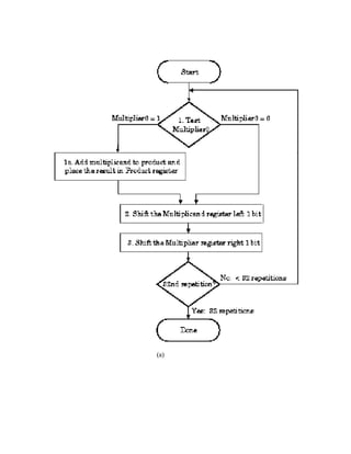
The second version of this algorithm is shown in Figure 3.16. Here, the product is shifted with
respect to the multiplier, and the multiplicand is shifted after the product register has been
shifted. A 64-bit register is used to store both the multiplicand and the product.](https://image.slidesharecdn.com/modifiedbooth-190717135919/85/Modified-booth-37-320.jpg)
![(b)
Figure 3.16. Second version of pencil-and-paper multiplication of 32-bit Boolean number
representations: (a) algorithm, and (b) schematic diagram of ALU circuitry - adapted from
[Maf01].
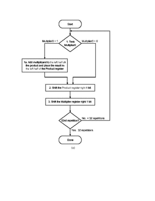
The final version puts results in the product register if and only if the least significant bit of the
product produced on the previous iteration is one-valued. The product register only is shifted.
This reduces by approximately 50 percent the amount of shifting that has to be done, which
reduces time and hardware requirements. The algorithm and ALU schematic diagram is shown in
Figure 3.17.](https://image.slidesharecdn.com/modifiedbooth-190717135919/85/Modified-booth-39-320.jpg)
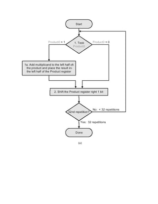
![(b)
Figure 3.17. Third version of pencil-and-paper multiplication of 32-bit Boolean number
representations: (a) algorithm, and (b) schematic diagram of ALU circuitry - adapted from
[Maf01].
Thus, we have the following shift-and-add scheme for multiplication:
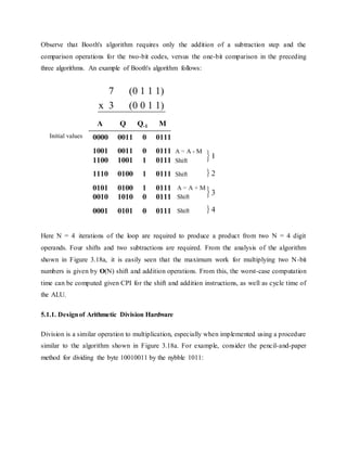
The preceding algorithms and circuitry does not hold for signed multiplication, since the
bits of the multiplier no longer correspond to shifts of the multiplicand. The following example is
illustrative:](https://image.slidesharecdn.com/modifiedbooth-190717135919/85/Modified-booth-41-320.jpg)
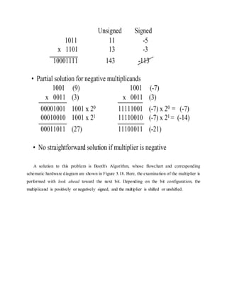
![(a)
(b)
Figure 3.18. Booth's procedure for multiplication of 32-bit Boolean number representations: (a)
algorithm, and (b) schematic diagram of ALU circuitry - adapted from [Maf01].](https://image.slidesharecdn.com/modifiedbooth-190717135919/85/Modified-booth-43-320.jpg)
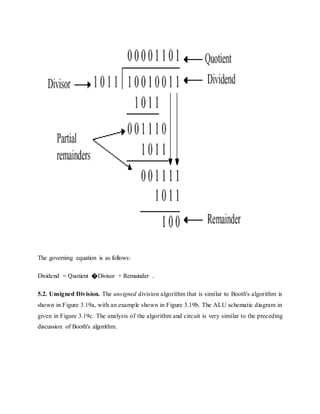
![(c)
Figure 3.19. Division of 32-bit Boolean number representations: (a) algorithm, (b) example
using division of the unsigned integer 7 by the unsigned integer 3, and (c) schematic diagram of
ALU circuitry - adapted from [Maf01].
5.2.1. Signed Division. With signed division, we negate the quotient if the signs of the divisor
and dividend disagree. The remainder and the dividend must have the same signs. The governing
equation is as follows:
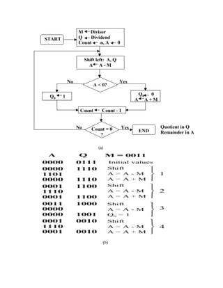
Remainder = Dividend - (Quotient �Divisor) ,](https://image.slidesharecdn.com/modifiedbooth-190717135919/85/Modified-booth-47-320.jpg)
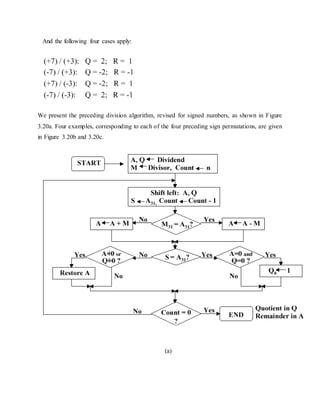
![(b)
(c)
Figure 3.20. Division of 32-bit Boolean number representations: (a) algorithm, and (b,c)
examples using division of +7 or -7 by the integer +3 or -3; adapted from [Maf01].](https://image.slidesharecdn.com/modifiedbooth-190717135919/85/Modified-booth-49-320.jpg)
![5.2.2. Division in MIPS. MIPS supports multiplication and division using existing hardware,
primarily the ALU and shifter. MIPS needs one extra hardware component - a 64-bit register
able to support sll and sra instructions. The upper (high) 32 bits of the register contains the
remainder resulting from division. This is moved into a register in the MIPS register stack (e.g.,
$t0) by the mfhi command. The lower 32 bits of the 64-bit register contains the quotient
resulting from division. This is moved into a register in the MIPS register stack by the mflo
command.
In MIPS assembly language code, signed division is supported by the div instruction and
unsigned division, by the divu instruction. MIPS hardware does not check for division by zero.
Thus, divide-by-zero exception must be detected and handled in system software. A similar
comment holds for overflow or underflow resulting from division.
Figure 3.21 illustrates the MIPS ALU that supports integer arithmetic operations (+,-,x,/).
Figure 3.21. MIPS ALU supporting the integer arithmetic operations (+,-,x,/), adapted from
[Maf01].](https://image.slidesharecdn.com/modifiedbooth-190717135919/85/Modified-booth-50-320.jpg)
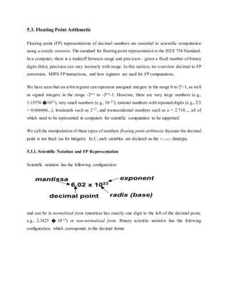
![recommended approach to NaNs, especially for software designers or engineers early in their
respective careers, is not to use NaNs.
Another variant of FP representation is denormalized numbers, also called denorms. These
number representations were developed to remedy the problem of a gap among representable FP
numbers near zero. For example, the smallest positive number is x = 1.00... � 2-127, and the
second smallest positive number is y = 1.0012 �2-127 = 2-127 + 2-150. This implies that the gap
between zero and x is 2-127 and that the gap between x and y is 2-150, as shown in Figure 3.22a.
(a) (b)
Figure 3.22. Denorms: (a) Gap between zero and 2-127, and (b) Denorms close this gap - adapted
from [Maf01].
This situation can be remedied by omitting the leading one from the significand, thereby
denormalizing the FP representation. The smallest positive number is now the denorm 0.0...1 �
2-127 = 2-150, and the second smallest positive number is 2-149.
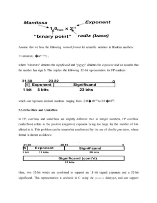
5.3.4. FP Arithmetic
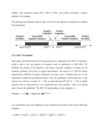
Applying mathematical operations to real numbers implies that some error will occur due to the
floating point representation. This is due to the fact that FP addition and subtraction are not
associative, because the FP representation is only an approximation to a real number.](https://image.slidesharecdn.com/modifiedbooth-190717135919/85/Modified-booth-56-320.jpg)

![Figure 3.23. MIPS ALU supporting floating point addition, adapted from [Maf01].
The use of floating point operations in MIPS assembly code is described in the following simple
example, which implements a C program designed to convert Fahrenheit temperatures to Celsius.](https://image.slidesharecdn.com/modifiedbooth-190717135919/85/Modified-booth-59-320.jpg)
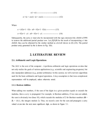
![6.1 EXPERIMENTAL RESULTS
For comparison, we have implemented several MBE multipliers whose partial
product arrays are generated by using different approaches. Except for a few of partial product
bits that are generated by different schemes to regularize the partial product array, the other
partial product bits are generated by using the similar method and circuits for all multipliers. In
addition, the partial product array of each multiplier is reduced by a Wallace tree scheme, and a
carry look-ahead adder is used for the final addition. These multipliers were modeled in Verilog
HDL and synthesized by using Synopsys Design Compiler with an Artisan TSMC 0.18-μm 1.8-
V standard cell library. The synthesized netlists were then fed into Cadence SOC Encounter to
perform placement and routing [15]. Delay estimates were obtained after RC extraction from the
placed and routed netlists. Power dissipation was estimated from the same netlists by feeding
them into Synopsys Nanosim to perform full transistor-level power simulation at a clock
frequency of 50 MHz with 5000 random input patterns. The implementation results, including
the hardware area, critical path delay, and power consumption for these multipliers with n = 8,
16, and 32, are listed in Table IV, where CBMa, CBMb [7], and CBMc [8] denote the MBE
multipliers with the partial product array shown in Fig. 1(a)–(c), respectively. Moreover, A(−),
D(−), and P(−) denote the area, delay, andpower decrements when compared with the CBMa
multiplier.
TABLE IV
EXPERIMENTAL RESULTS OF MBEMULTIPLIERS](https://image.slidesharecdn.com/modifiedbooth-190717135919/85/Modified-booth-65-320.jpg)
![7.PROGRAM CODE
module booth_multi_tb ;
wire [15:0] dout ;
reg [7:0] x ;
reg [7:0] y ;
booth_multi
DUT (
.dout (dout ) ,
.x (x ) ,
.y (y ) );
initial
fork
x=8'b00001010;
y=8'b00001010;
join
endmodule
module fulladd (carry,sum,a,b,c);
output carry;
output sum;
input a;
input b;
input c;
assign carry= (a&b)|(a&c)|(c|a);
assign sum = a^b^c;
endmodule
module halfadd (carry,sum,a,b);
output carry;
output sum;
input a;
input b;
assign carry= (a&b);
assign sum = a^b;
endmodule
module negout (b2i1,b2i,b2i_1,aj,aj_1,pij,negi);
input b2i1;
input b2i;
input b2i_1;
input aj;
input aj_1;](https://image.slidesharecdn.com/modifiedbooth-190717135919/85/Modified-booth-69-320.jpg)
![module pij_out1 (x2i1,x2i,x2i_1,yi,yi_1,pij);
input x2i1;
input x2i;
input x2i_1;
input yi;
input yi_1;
output pij;
assign negi = x2i1 & ((~x2i) | (~x2i_1));
assign onebar = ~(x2i^ x2i_1);
assign w1= ((~x2i1)& x2i & x2i_1);
assign w2= (x2i1& (~x2i) &(~x2i_1));
assign twobar = ~(w1|w2);
assign w3 = twobar|yi_1;
assign w4 = ~(yi^x2i1);
assign w5 = onebar|w4;
assign pij = ~(w3&w4);
endmodule
module pij_out2 (x2i1,x2i,x2i_1,yi,yi_1,pij);
input x2i1;
input x2i;
input x2i_1;
input yi;
input yi_1;
output pij;
assign negi = x2i1 & ((~x2i) | (~x2i_1));
assign onebar = (x2i^ x2i_1);
assign w1= ((~x2i1)& x2i & x2i_1);
assign w2= (x2i1& (~x2i) &(~x2i_1));
assign twobar = (w1|w2);
assign w3 = onebar & yi;
assign w4 = yi_1 & twobar;
assign w5 = ~(w3|w4);
assign pij = ~(w5^negi);
endmodule
//------------------ Y x X -----------------------//
module booth_multi (x,y,dout);
input [7:0] y;
input [7:0] x;
output[15:0] dout;
wire [7:0]pp1;](https://image.slidesharecdn.com/modifiedbooth-190717135919/85/Modified-booth-71-320.jpg)
![wire [7:0]pp2;
wire [7:0]pp3;
wire [7:0]pp4;
wire [15:0] ppf1;
wire [15:0] ppf2;
wire [15:0] ppf3;
wire [15:0] ppf4;
wire [15:0] const;
wire [3:0]neg;
////////i=0; j=0;
pij_out2 p00(.x2i1(x[1]),
.x2i(x[0]),
.x2i_1(1'b0),
.yi(y[0]),
.yi_1(1'b0),
.pij(pp1[0])
);
////////i=0; j=1;
pij_out2 p01(.x2i1(x[1]),
.x2i(x[0]),
.x2i_1(1'b0),
.yi(y[1]),
.yi_1(y[0]),
.pij(pp1[1])
);
////////i=0; j=2;
pij_out2 p02(.x2i1(x[1]),
.x2i(x[0]),
.x2i_1(1'b0),
.yi(y[2]),
.yi_1(y[1]),
.pij(pp1[2])
);
////////i=0; j=3;
pij_out2 p03(.x2i1(x[1]),
.x2i(x[0]),
.x2i_1(1'b0),
.yi(y[3]),
.yi_1(y[2]),
.pij(pp1[3])
);
pij_out2 p04(.x2i1(x[1]),
.x2i(x[0]),
.x2i_1(1'b0),
.yi(y[4]),
.yi_1(y[3]),
.pij(pp1[4])
);
pij_out2 p05(.x2i1(x[1]),
.x2i(x[0]),](https://image.slidesharecdn.com/modifiedbooth-190717135919/85/Modified-booth-72-320.jpg)
![.x2i_1(1'b0),
.yi(y[5]),
.yi_1(y[4]),
.pij(pp1[5])
);
pij_out2 p06(.x2i1(x[1]),
.x2i(x[0]),
.x2i_1(1'b0),
.yi(y[6]),
.yi_1(y[5]),
.pij(pp1[6])
);
pij_out2 p07(.x2i1(x[1]),
.x2i(x[0]),
.x2i_1(1'b0),
.yi(y[7]),
.yi_1(y[6]),
.pij(pp1[7])
);
//--------------------------pp2
////////i=1; j=0;
pij_out2 p10(.x2i1(x[3]),
.x2i(x[2]),
.x2i_1(x[1]),
.yi(y[0]),
.yi_1(1'b0),
.pij(pp2[0])
);
////////i=1; j=1;
pij_out2 p11(.x2i1(x[3]),
.x2i(x[2]),
.x2i_1(x[1]),
.yi(y[1]),
.yi_1(y[0]),
.pij(pp2[1])
);
////////i=1; j=2;
pij_out2 p12(.x2i1(x[3]),
.x2i(x[2]),
.x2i_1(x[1]),
.yi(y[2]),
.yi_1(y[1]),
.pij(pp2[2])
);
pij_out2 p13(.x2i1(x[3]),
.x2i(x[2]),
.x2i_1(x[1]),
.yi(y[3]),](https://image.slidesharecdn.com/modifiedbooth-190717135919/85/Modified-booth-73-320.jpg)
![.yi_1(y[2]),
.pij(pp2[3])
);
pij_out2 p14(.x2i1(x[3]),
.x2i(x[2]),
.x2i_1(x[1]),
.yi(y[4]),
.yi_1(y[3]),
.pij(pp2[4])
);
pij_out2 p15(.x2i1(x[3]),
.x2i(x[2]),
.x2i_1(x[1]),
.yi(y[5]),
.yi_1(y[4]),
.pij(pp2[5])
);
pij_out2 p16(.x2i1(x[3]),
.x2i(x[2]),
.x2i_1(x[1]),
.yi(y[6]),
.yi_1(y[5]),
.pij(pp2[6])
);
pij_out2 p17(.x2i1(x[3]),
.x2i(x[2]),
.x2i_1(x[1]),
.yi(y[7]),
.yi_1(y[6]),
.pij(pp2[7])
);
//--------------------pp3---------------------------------//
// i=2 j=0;
pij_out2 p20(.x2i1(x[5]),
.x2i(x[4]),
.x2i_1(x[3]),
.yi(y[0]),
.yi_1(1'b0),
.pij(pp3[0])
);
pij_out2 p21(.x2i1(x[5]),
.x2i(x[4]),
.x2i_1(x[3]),
.yi(y[1]),
.yi_1(y[0]),
.pij(pp3[1])
);
pij_out2 p22(.x2i1(x[5]),
.x2i(x[4]),
.x2i_1(x[3]),
.yi(y[2]),](https://image.slidesharecdn.com/modifiedbooth-190717135919/85/Modified-booth-74-320.jpg)
![.yi_1(y[1]),
.pij(pp3[2])
);
pij_out2 p23(.x2i1(x[5]),
.x2i(x[4]),
.x2i_1(x[3]),
.yi(y[3]),
.yi_1(y[2]),
.pij(pp3[3])
);
pij_out2 p24(.x2i1(x[5]),
.x2i(x[4]),
.x2i_1(x[3]),
.yi(y[4]),
.yi_1(y[3]),
.pij(pp3[4])
);
pij_out2 p25(.x2i1(x[5]),
.x2i(x[4]),
.x2i_1(x[3]),
.yi(y[5]),
.yi_1(y[4]),
.pij(pp3[5])
);
pij_out2 p26(.x2i1(x[5]),
.x2i(x[4]),
.x2i_1(x[3]),
.yi(y[6]),
.yi_1(y[5]),
.pij(pp3[6])
);
pij_out2 p27(.x2i1(x[5]),
.x2i(x[4]),
.x2i_1(x[3]),
.yi(y[7]),
.yi_1(y[6]),
.pij(pp3[7])
);
//--- i=3 j=0 ------//
pij_out2 p30(.x2i1(x[7]),
.x2i(x[6]),
.x2i_1(x[5]),
.yi(y[0]),](https://image.slidesharecdn.com/modifiedbooth-190717135919/85/Modified-booth-75-320.jpg)
![.yi_1(1'b0),
.pij(pp4[0])
);
pij_out2 p31(.x2i1(x[7]),
.x2i(x[6]),
.x2i_1(x[5]),
.yi(y[1]),
.yi_1(y[0]),
.pij(pp4[1])
);
pij_out2 p32(.x2i1(x[7]),
.x2i(x[6]),
.x2i_1(x[5]),
.yi(y[2]),
.yi_1(y[1]),
.pij(pp4[2])
);
pij_out2 p33(.x2i1(x[7]),
.x2i(x[6]),
.x2i_1(x[5]),
.yi(y[3]),
.yi_1(y[2]),
.pij(pp4[3])
);
pij_out2 p34(.x2i1(x[7]),
.x2i(x[6]),
.x2i_1(x[5]),
.yi(y[4]),
.yi_1(y[3]),
.pij(pp4[4])
);
pij_out2 p35(.x2i1(x[7]),
.x2i(x[6]),
.x2i_1(x[5]),
.yi(y[5]),
.yi_1(y[4]),
.pij(pp4[5])
);
pij_out2 p36(.x2i1(x[7]),
.x2i(x[6]),
.x2i_1(x[5]),
.yi(y[6]),
.yi_1(y[5]),
.pij(pp4[6])
);](https://image.slidesharecdn.com/modifiedbooth-190717135919/85/Modified-booth-76-320.jpg)
![pij_out2 p37(.x2i1(x[7]),
.x2i(x[6]),
.x2i_1(x[5]),
.yi(y[7]),
.yi_1(y[6]),
.pij(pp4[7])
);
neggen u1 (
.x2i1(x[1]),.x2i(x[0]),.x2i_1(1'b0),.negi(neg[0])
);
neggen u2 (
.x2i1(x[3]),.x2i(x[2]),.x2i_1(x[1]),.negi(neg[1])
);
neggen u3 (
.x2i1(x[5]),.x2i(x[4]),.x2i_1(x[3]),.negi(neg[2])
);
neggen u4 (
.x2i1(x[7]),.x2i(x[6]),.x2i_1(x[5]),.negi(neg[3])
);
assign ppf1 = {5'd0,(~pp1[7]),pp1[7],pp1[7] ,pp1};
assign ppf2 = {4'd0,1'b1,(~pp2[7]),pp2,1'b0,neg[0]};
assign ppf3 = {2'd0,1'b1,(~pp3[7]),pp3,1'b0,neg[1],2'd0};
assign ppf4 = {1'b1,(~pp4[7]),pp4,1'd0,neg[2],4'd0};
assign const = {9'd0,neg[3],6'd0};
assign dout = ppf1+ppf2+ppf3+ppf4+const;
endmodule](https://image.slidesharecdn.com/modifiedbooth-190717135919/85/Modified-booth-77-320.jpg)

![References
[1][Maf01] Mafla, E. Course Notes, CDA3101, at URL http://www.cise.ufl.edu/~emafla/ (as-of
11 Apr 2001).
[2][Pat98] Patterson, D.A. and J.L. Hennesey. Computer Organization and Design: The
Hardware/Software Interface, Second Edition, San Francisco, CA: Morgan Kaufman (1998).
[3]. S. Wallace, “A suggestion for parallel multipliers,” IEEE Trans. Electron.Comput., vol. EC-
13, no. 1, pp. 14–17, Feb. 1964.
[4] O. Hasan and S. Kort, “Automated formal synthesis of Wallace tree multipliers,”in Proc.
50th Midwest Symp. Circuits Syst., 2007, pp. 293–296.
[5] J. Fadavi-Ardekani, “M × N booth encoded multiplier generator using optimized Wallace
trees,” IEEE Trans. Very Large Scale Integr. (VLSI) Syst., vol. 1, no. 2, pp. 120–125, Jun. 1993.
[6] F. Elguibaly, “A fast parallel multiplier-accumulator using the modified Booth algorithm,”
IEEE Trans. Circuits Syst. II, Analog Digit. Signal Process., vol. 47, no. 9, pp. 902–908, Sep.
2000.
[7] K. Choi and M. Song, “Design of a high performance 32 × 32-bit multiplier with a novel sign
select Booth encoder,” in Proc. IEEE Int. Symp. Circuits Syst., 2001, vol. 2, pp. 701–704.
[8] Y. E. Kim, J. O. Yoon, K. J. Cho, J. G. Chung, S. I. Cho, and S. S. Choi, “Efficient design of
modified Booth multipliers for predetermined coefficients,” in Proc. IEEE Int. Symp. Circuits
Syst., 2006, pp. 2717–2720.
[9] W.-C. Yeh and C.-W. Jen, “High-speed booth encoded parallel multiplier design,” IEEE
Trans. Comput., vol. 49, no. 7, pp. 692–701, Jul. 2000.
[10] J.-Y. Kang and J.-L. Gaudiot, “A simple high-speed multiplier design,” IEEE Trans.
Comput., vol. 55, no. 10, pp. 1253–1258, Oct. 2006.](https://image.slidesharecdn.com/modifiedbooth-190717135919/85/Modified-booth-79-320.jpg)