Download to read offline

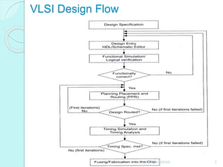
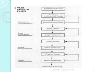
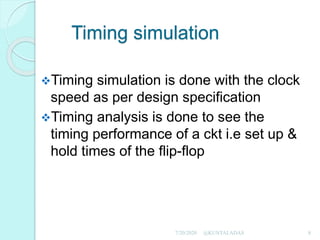
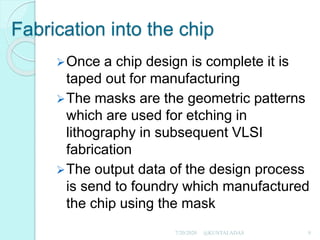


The VLSI design flow involves several steps: (1) specifying the design requirements, (2) entering the design using schematics or a hardware description language, (3) performing functional simulation to verify the logic, (4) planning placement and routing of components on the chip, (5) conducting timing simulation to check timing performance, and (6) fabricating the chip using the generated masks.