The document summarizes key details about the Intel 8086 microprocessor, including:
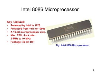
- It was released in 1978 and produced until the 1990s, with a clock speed of 5-10MHz and 40-pin DIP package.
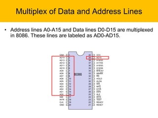
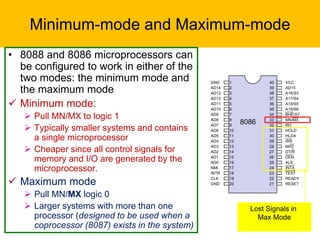
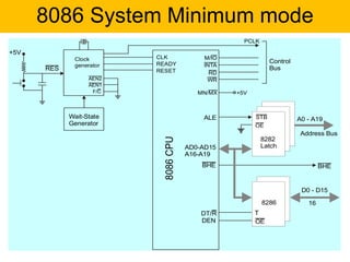
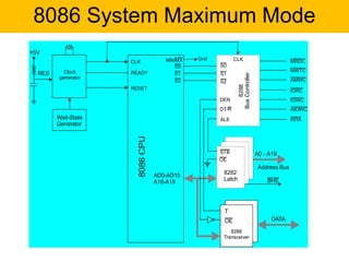
- It has a 16-bit architecture and multiplexed address/data lines. Systems using the 8086 can operate in minimum or maximum mode depending on the MN/MX pin setting.
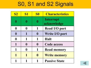
- The document describes the various pins of the 8086 chip, their functions, and how they are used to interface with memory and I/O devices in minimum and maximum mode systems.