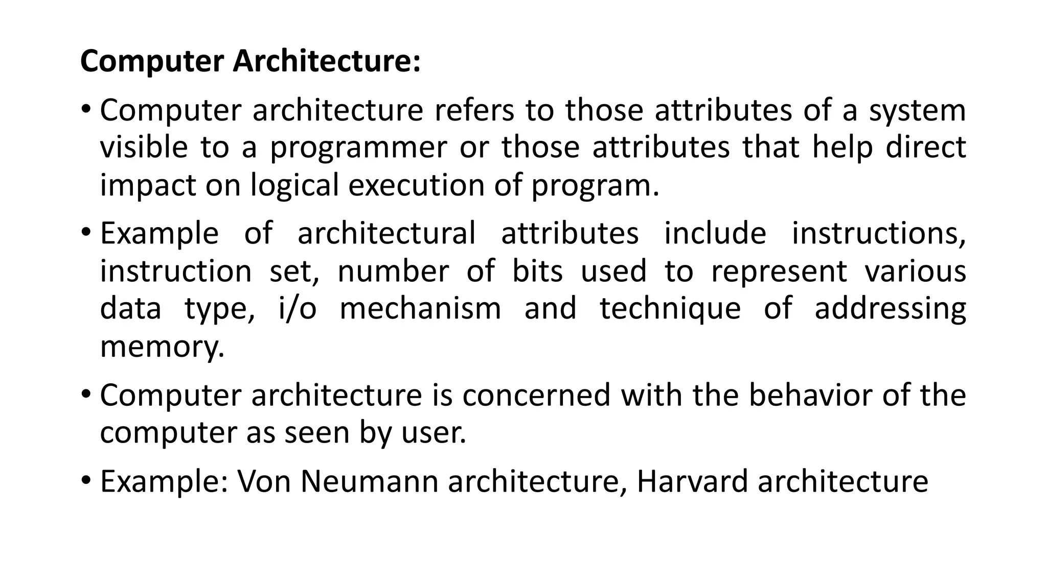
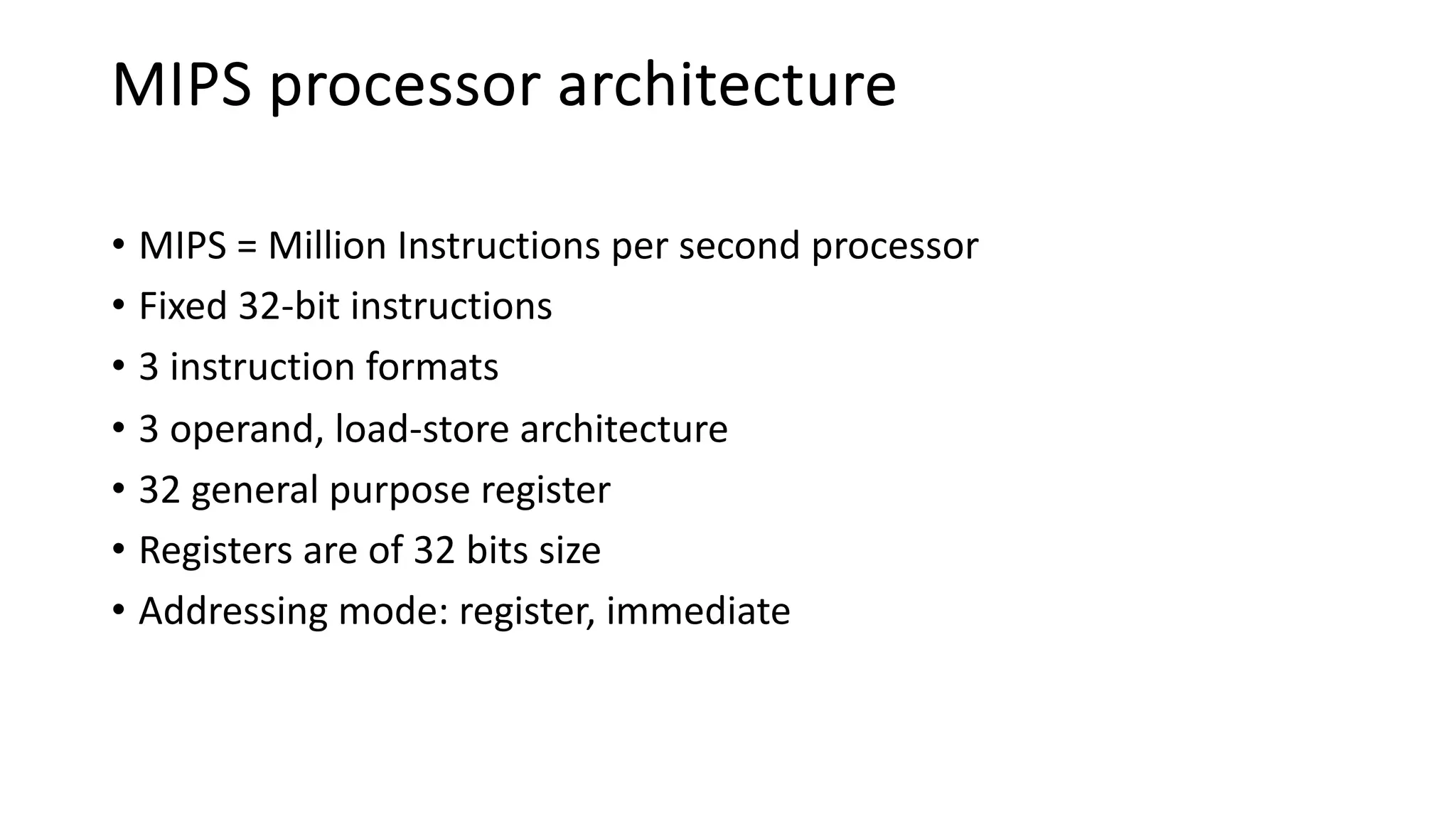
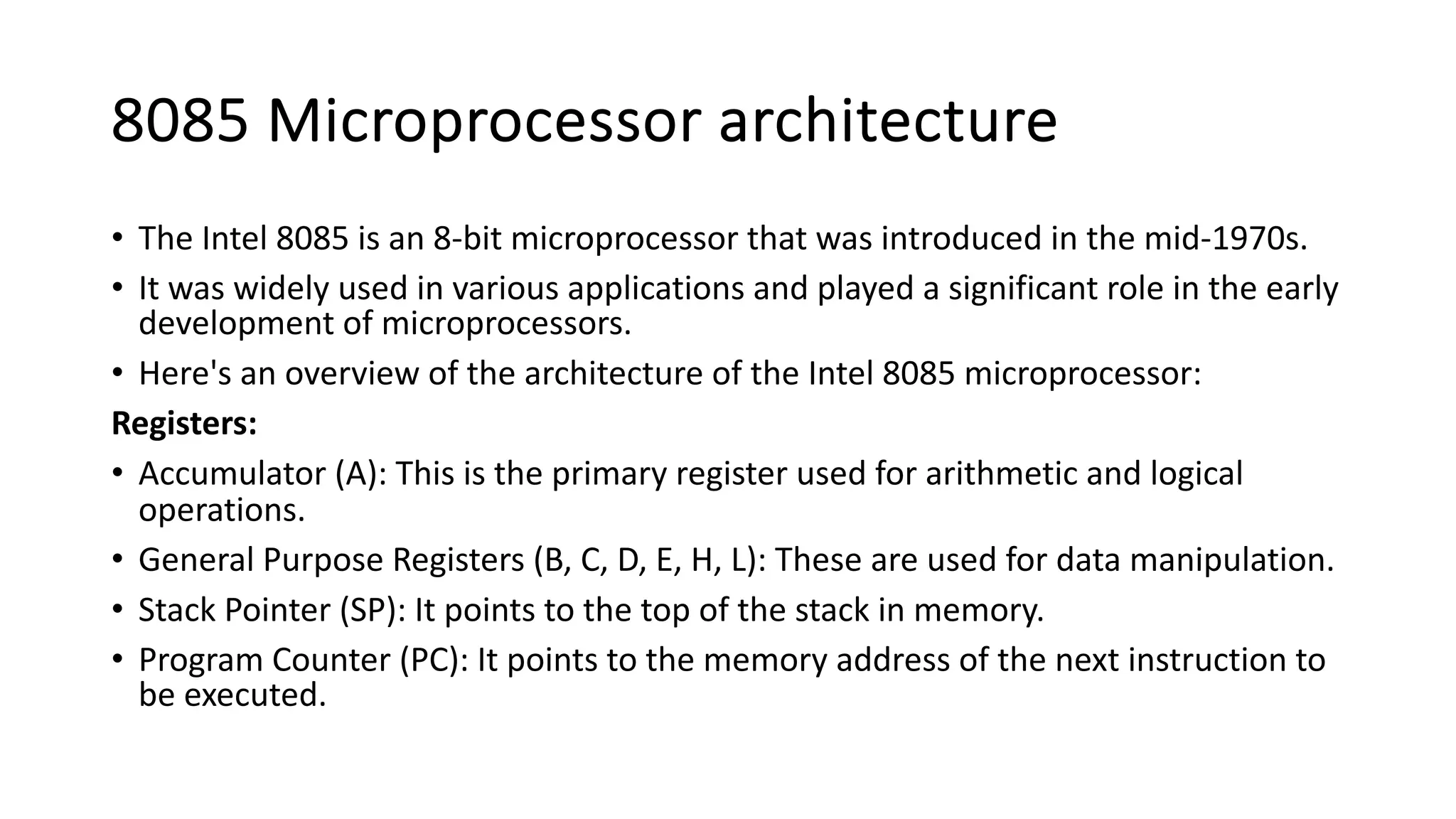
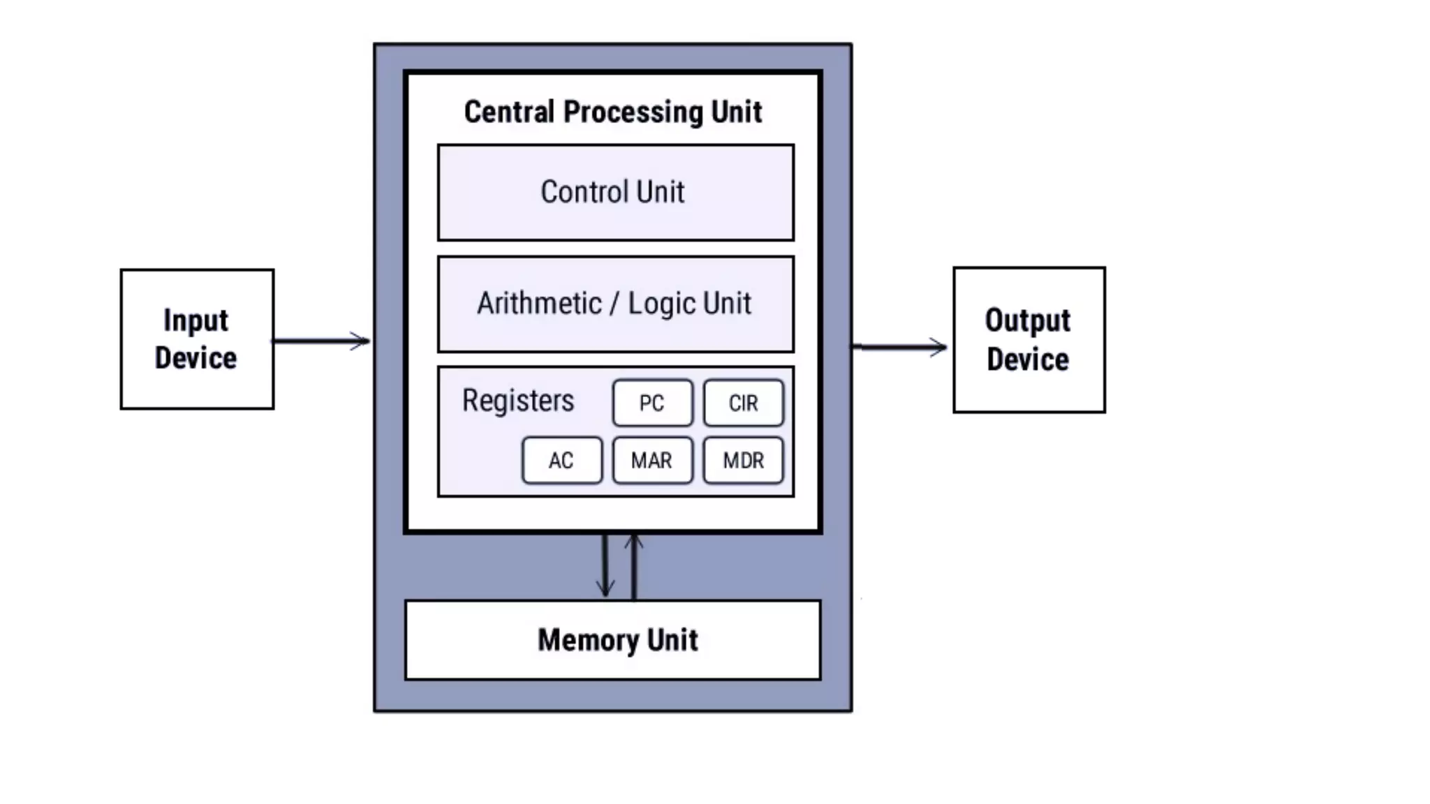
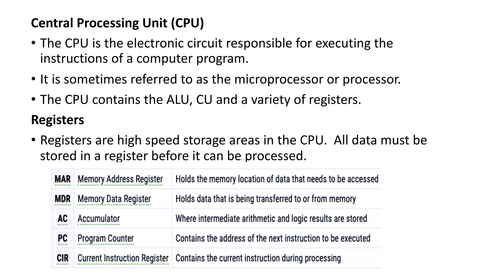
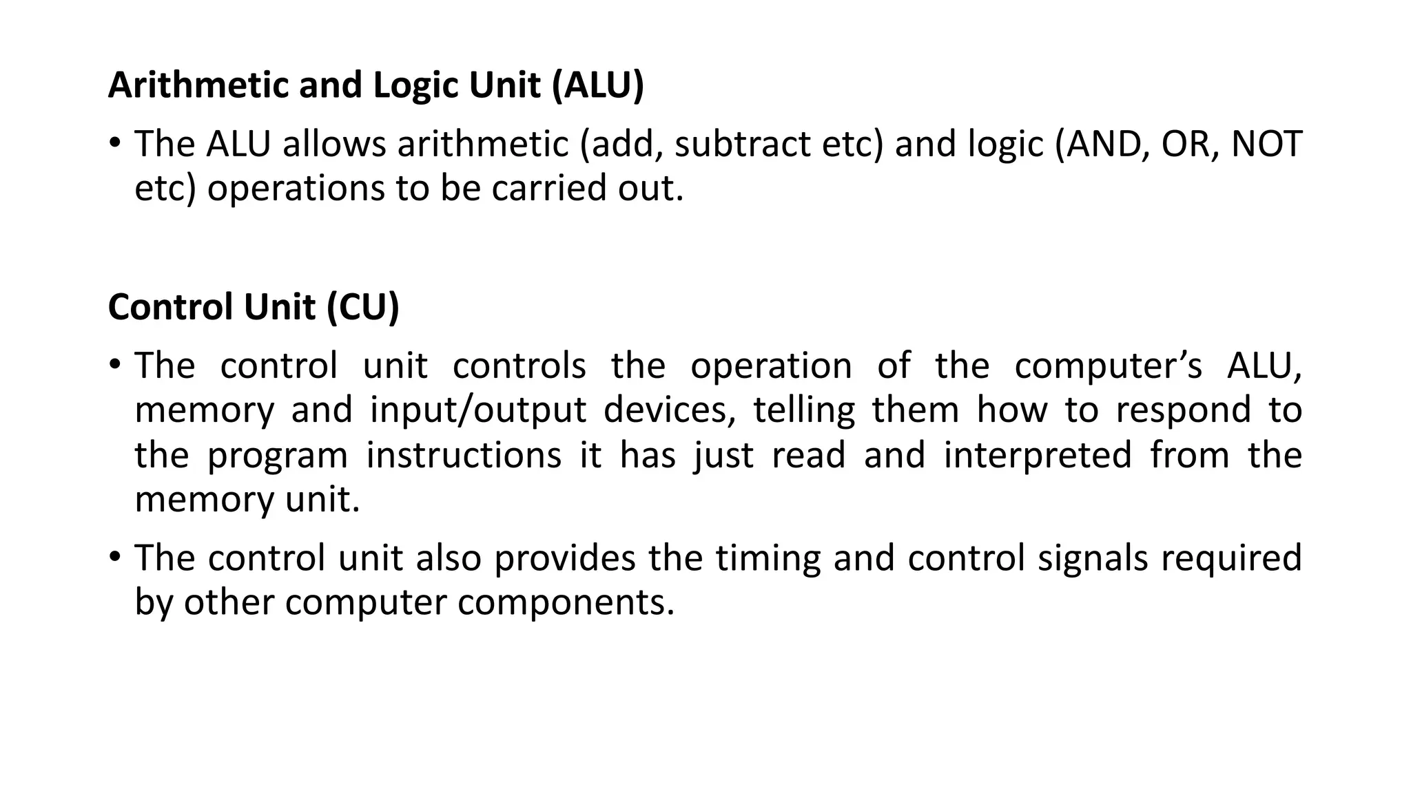
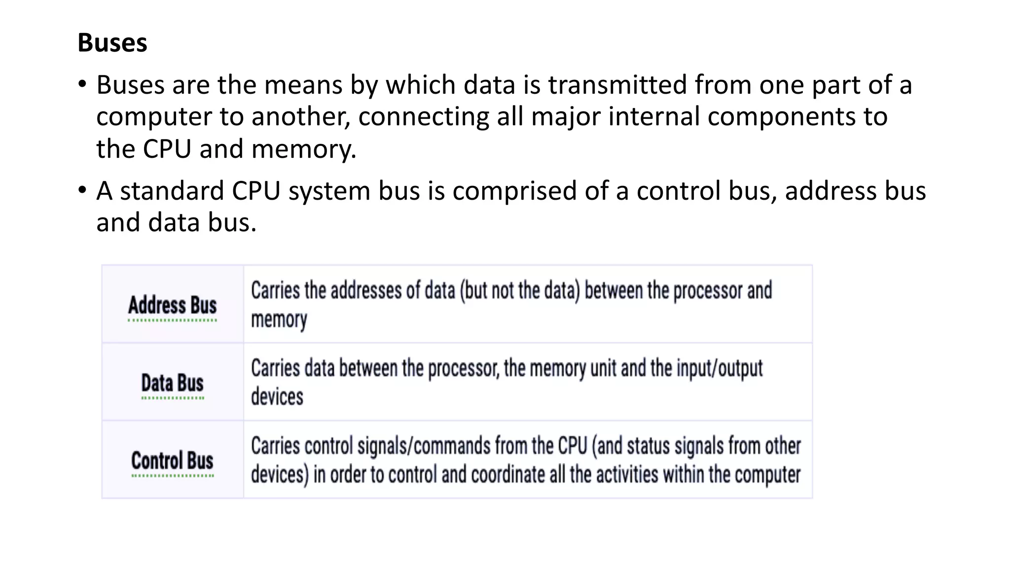
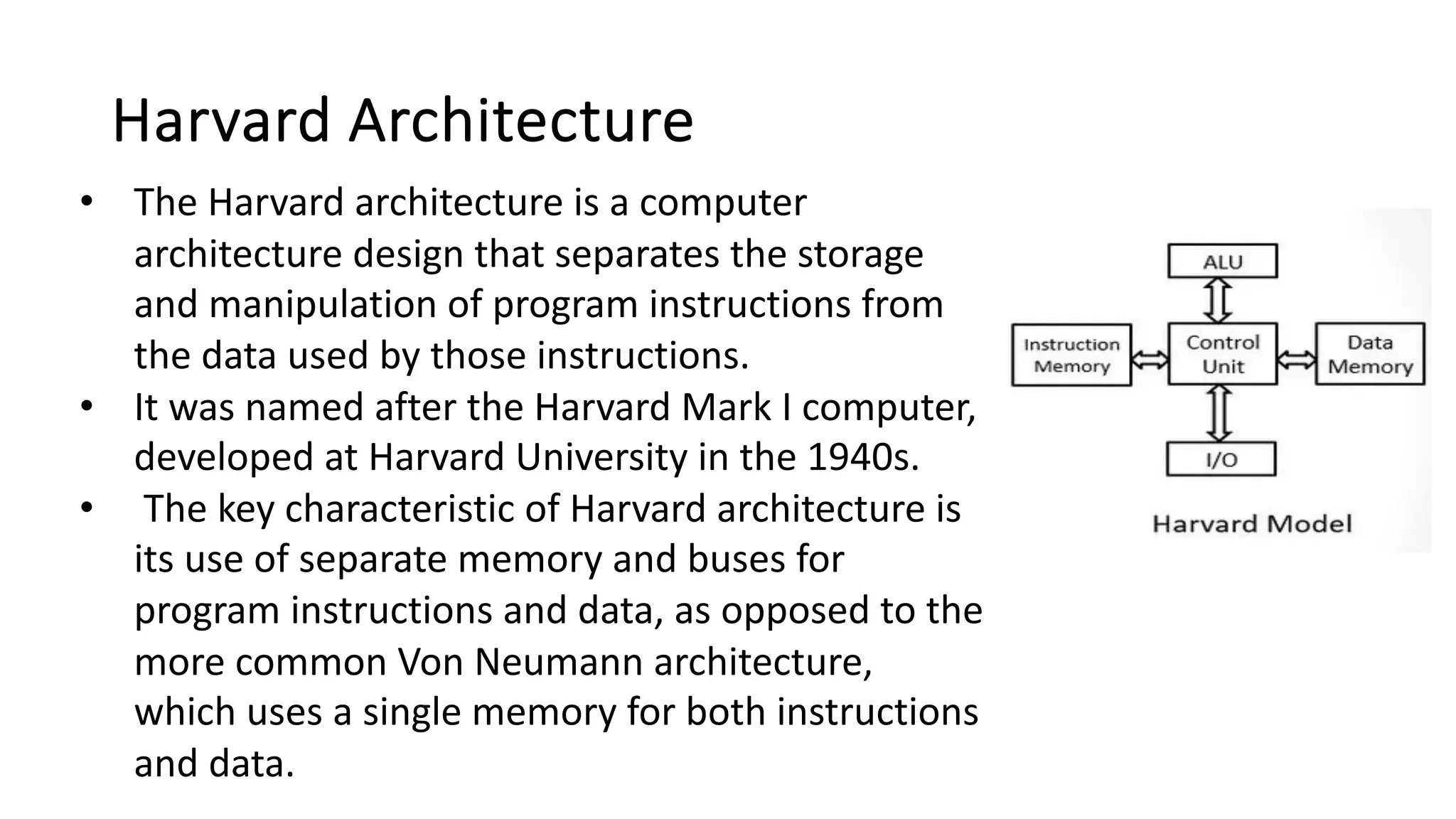
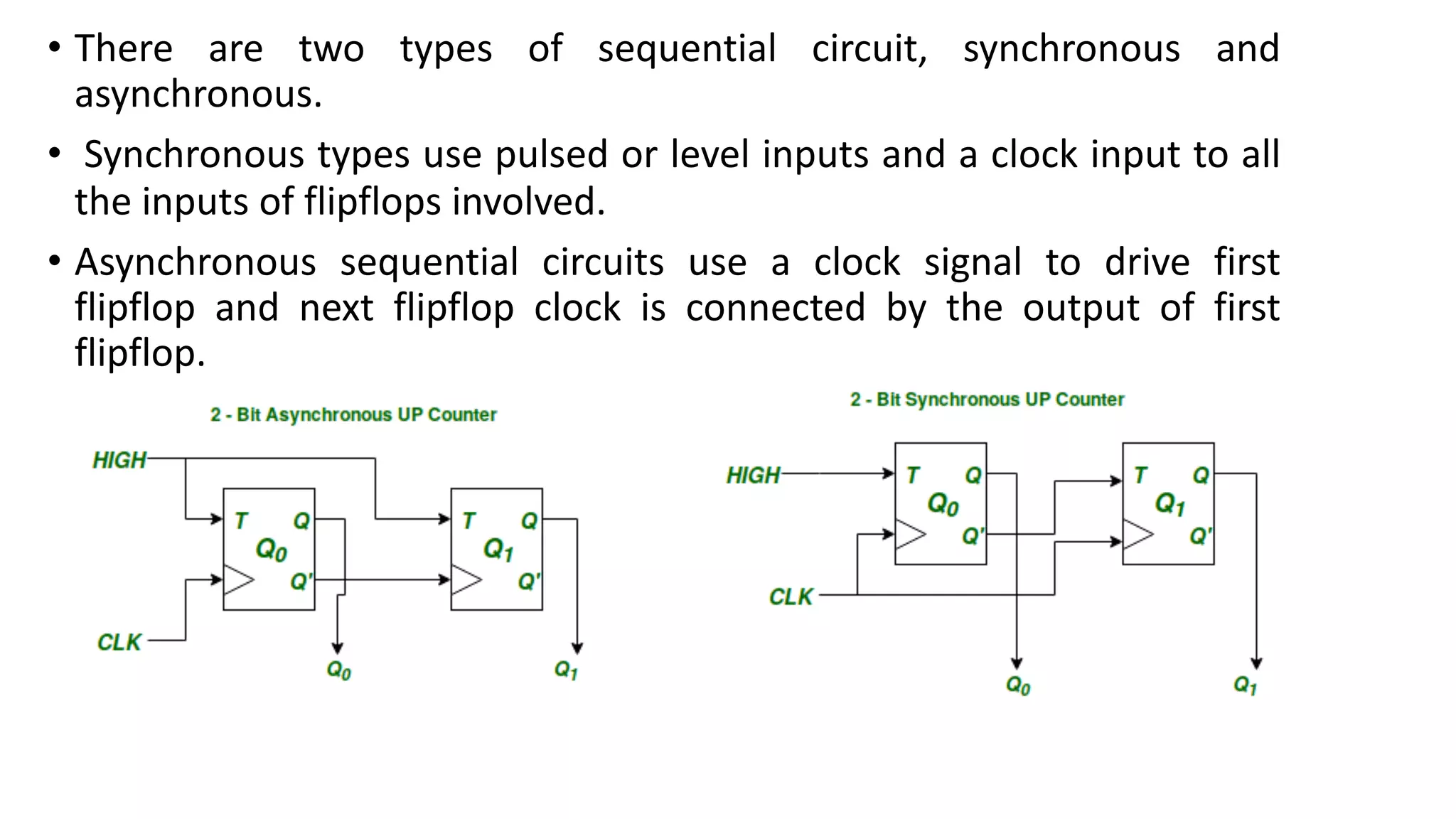
This document provides an overview of the syllabus for a course on computer architecture and organization. The course objectives are to build upon concepts from prior digital logic and computer foundation courses. The contents cover topics like basic computer structures, addressing methods, the processing unit, memory systems, and arithmetic operations. Examples of specific computer architectures discussed include the Von Neumann architecture, MIPS, 8085, and 8086 microprocessors. Key components of a computer like the CPU, ALU, control unit, registers, buses, and memory are also defined.
![Contents:
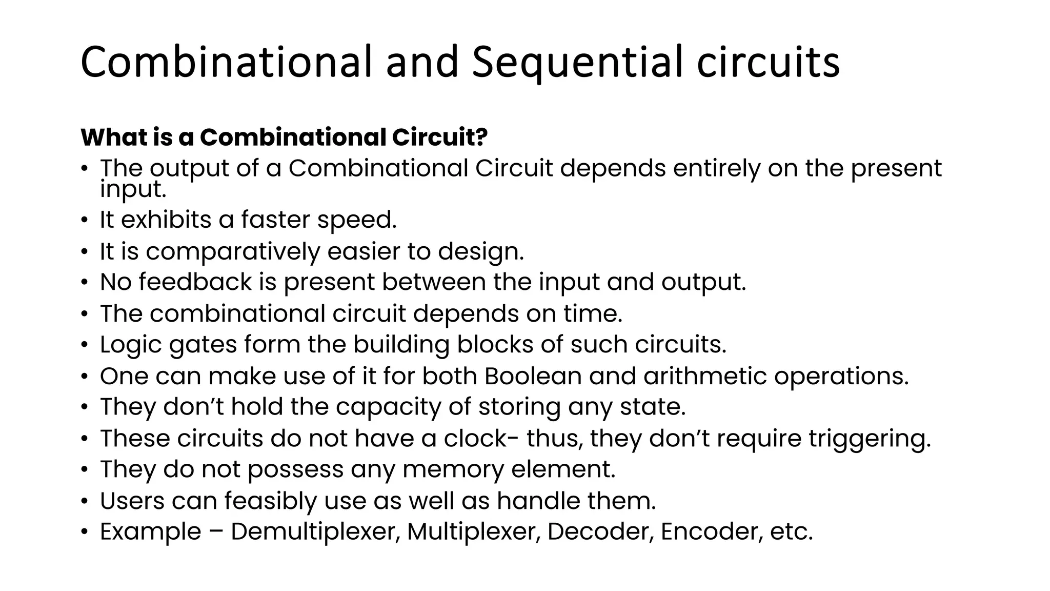
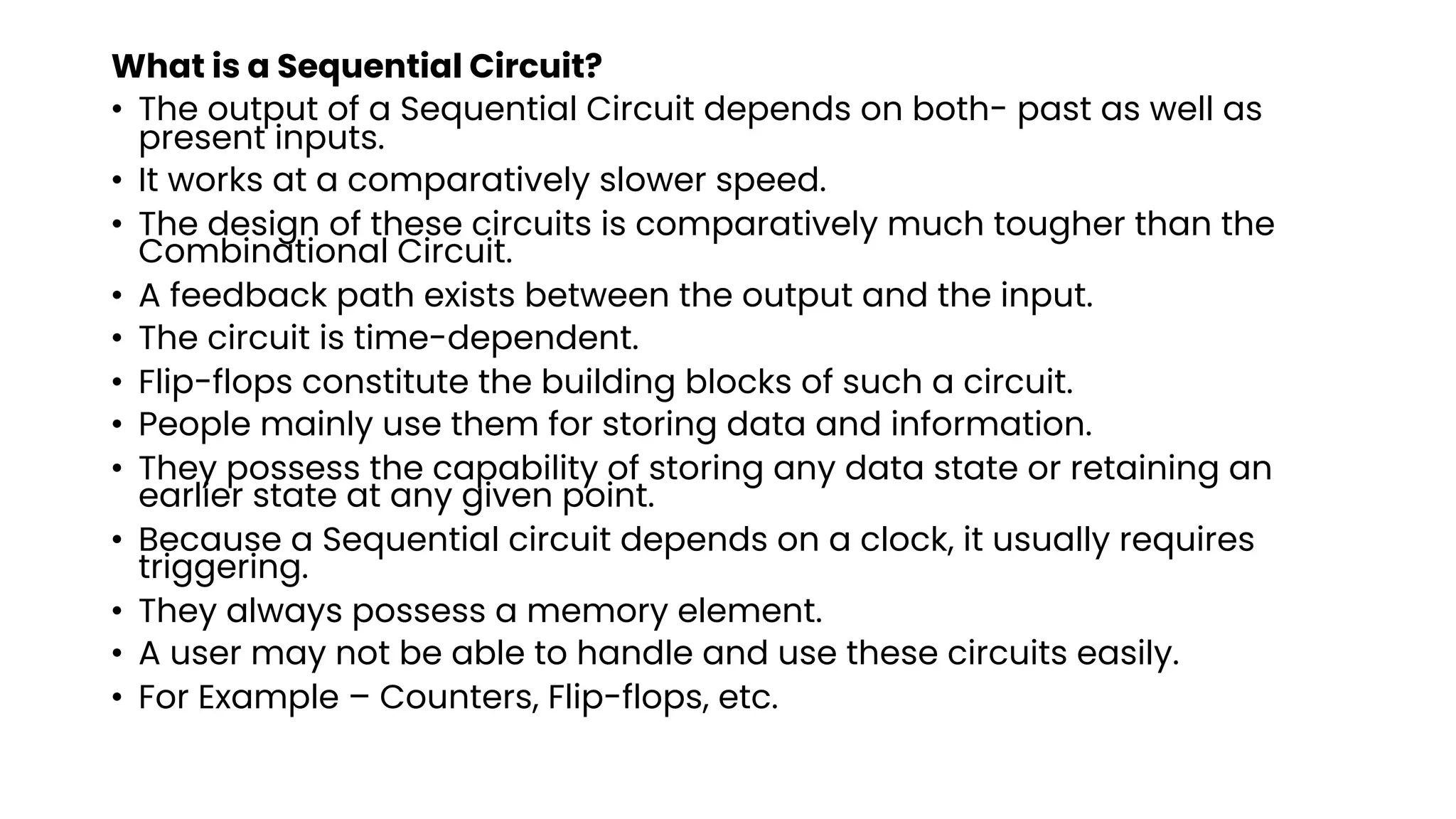
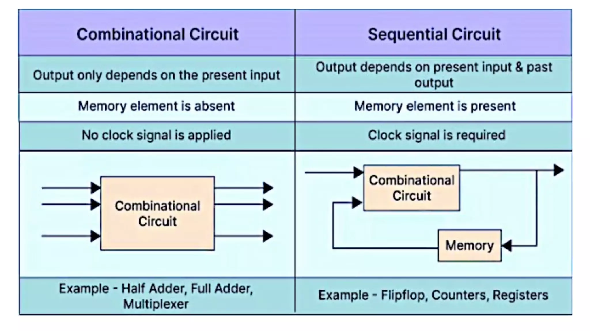
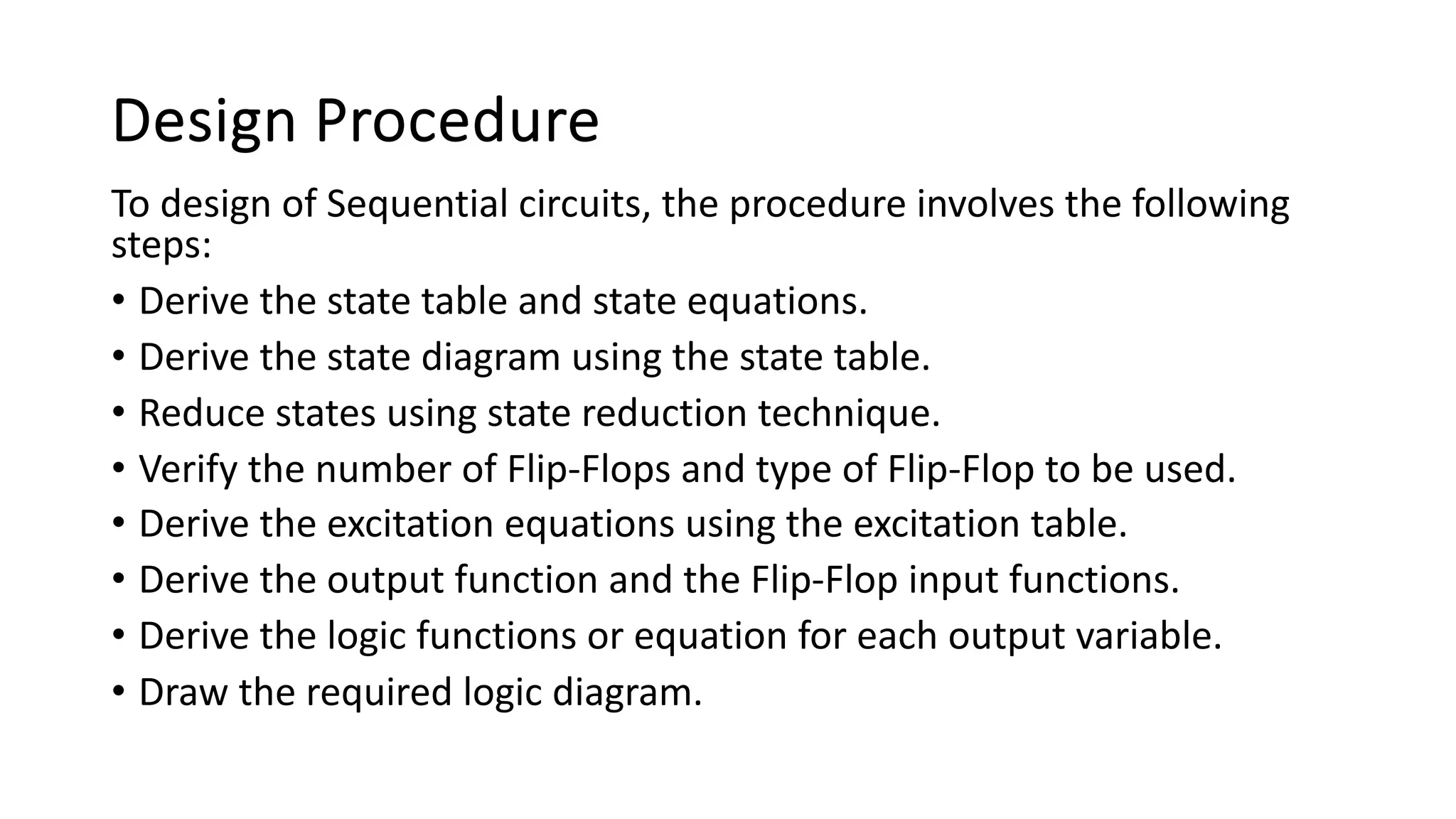
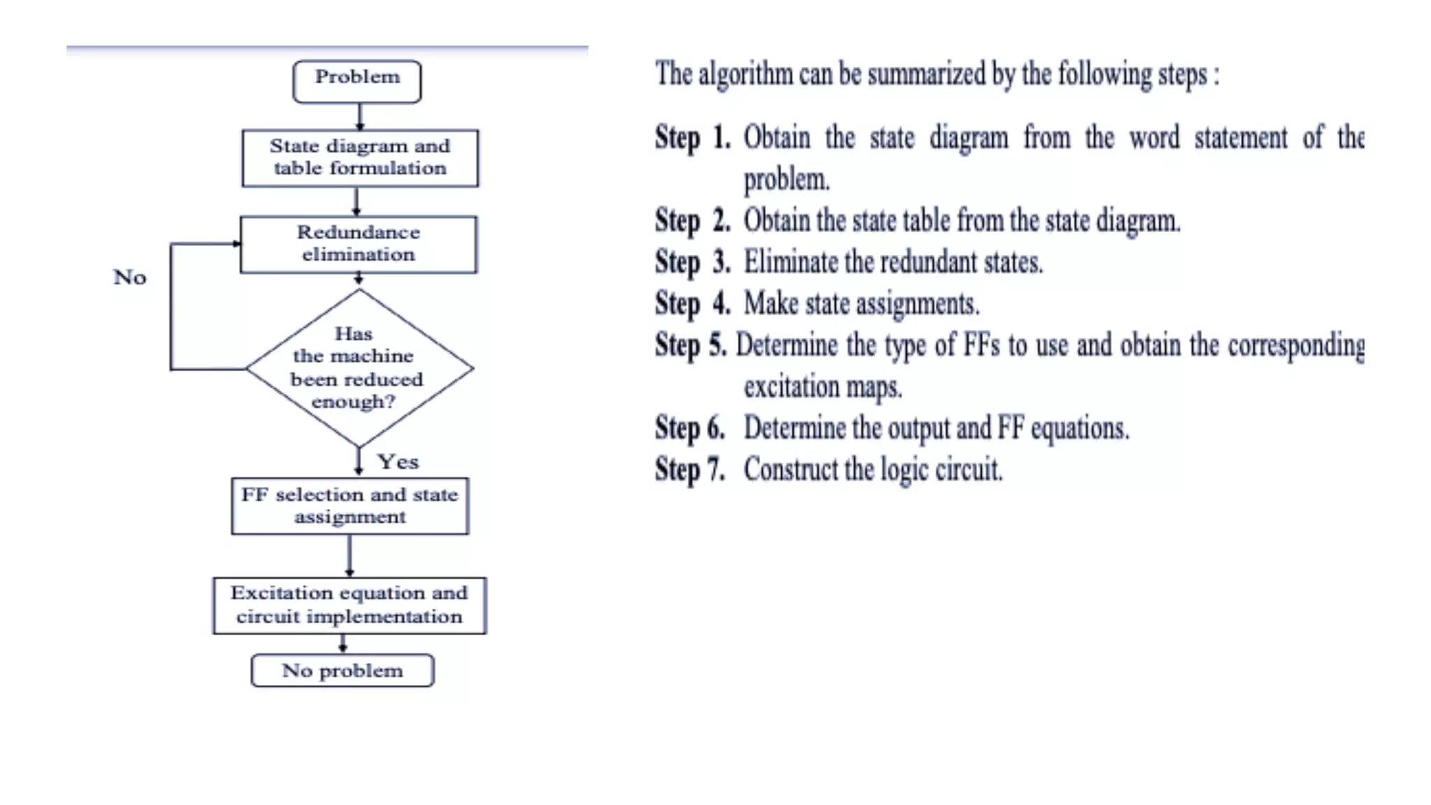
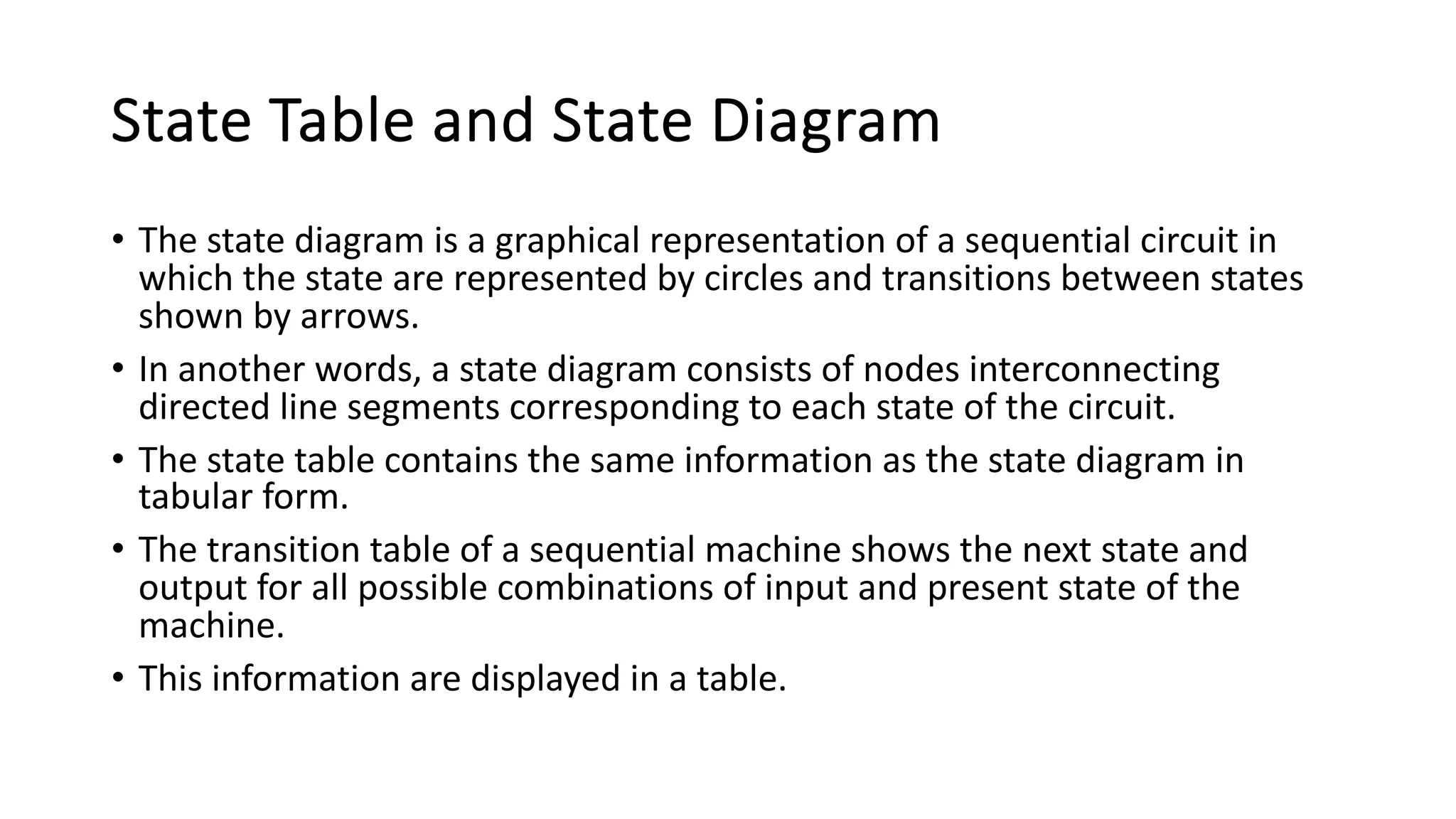
1. Basic Structures: Sequential circuits, design procedure, state table and state
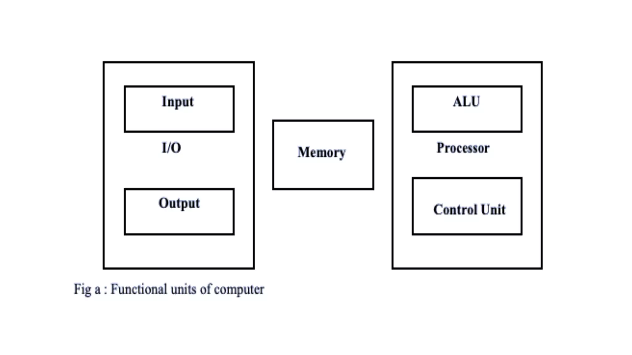
diagram Von Neumann architecture, stored program concepts and functional
units.[3 hrs.]
2. Addressing Methods and Programs: Programming view of a processor, data
types, and representation of data, arithmetic operations, basic operational
concepts, bus structures, instruction cycle and excitation cycle. [8 hrs.]
3. Processing Unit: Instruction formats: computer instruction, instruction length,
address instruction, arithmetic instruction, and logical instruction. [6 hrs.]
4. Addressing modes: General concepts, single-component addressing modes,
multi-component addressing modes, and position-independent code. [6 hrs.]
5. Input Output Organization: Basic principles of interrupt-driven I/O and DMA,
I/O operations, I/O programming, memory-mapped I/O, basic interrupt system,
direct memory access, DMA channel programming, and memory-mapped
screens.[6 hrs.]](https://image.slidesharecdn.com/unit1basicstructurecoa-231002082542-3f6e5b76/75/Unit-1-Basic-structureCOA-pdf-3-2048.jpg)
![6)Arithmetic: Magnitude comparator, complements, straight
subtraction, subtraction with complements, addition and subtraction
algorithms, hardware implementation, multiplication and division
algorithms, hardware implementation, and divide overflow [6 hrs.]
7) Memory System: Auxiliary memory: magnetic drum, magnetic disks,
and magnetic tapes; microcomputer. [4 hrs.]
8)Memory: RAM/ROM chips, memory address map, memory
connection to microprocessor; memory hierarchy; associative memory:
hardware organization, Match logic, read operation, write operation;
virtual memory: address space memory space, address mapping,
associative memory page table; cache memory: associative mapping,
direct mapping, set associative mapping; memory management
hardware [6 hrs.]](https://image.slidesharecdn.com/unit1basicstructurecoa-231002082542-3f6e5b76/75/Unit-1-Basic-structureCOA-pdf-4-2048.jpg)


![Unit 03 Computer and Internet Crime [5 hrs] v1.2.pdf](https://cdn.slidesharecdn.com/ss_thumbnails/unit03computerandinternetcrime5hrsv1-240428164706-fc842b5e-thumbnail.jpg?width=640&height=640&fit=bounds)