The document describes a thesis submitted for a Doctor of Philosophy degree that investigated optical time-division multiplexing (OTDM) techniques for high-speed local and wide area network interconnects. Specifically, it demonstrated a 40 Gbit/s optical TDMA network establishing 2.5 Gbit/s connections between computer workstations using single-mode fiber. The thesis explored different optical pulse sources for OTDM including gain-switched distributed feedback lasers and electroabsorption modulators. It also investigated techniques for pulse compression, modulation, multiplexing, and demultiplexing to enable fast reconfigurable high-bandwidth interconnects.


![List of Tables
2.1 Classification and properties of normal and anomalously dispersive
optical fibre. . . . . . . . . . . . . . . . . . . . . . . . . . . . . . . . . 37
3.1 Specification of dispersion decreasing fibre. . . . . . . . . . . . . . . . 92
3.2 Sampling oscilloscope channel jitter measurements. . . . . . . . . . . 98
3.3 Classification and properties of the various pulse sources described in
this chapter. . . . . . . . . . . . . . . . . . . . . . . . . . . . . . . . . 130
4.1 Non-linear optical properties and figure of merit of several material
systems. . . . . . . . . . . . . . . . . . . . . . . . . . . . . . . . . . . 154
5.1 Classification of switching speeds. . . . . . . . . . . . . . . . . . . . . 171
5.2 Optical fibre characteristics from ref. [8]. D, is the group delay disper-
sion; λo, is the zero-dispersion wavelength; θ, is the temperature; So, is
the dispersion slope. dλ/dθ|λ=λo , is the thermal coefficient term. NZ-
DSF: non-zero dispersion shifted fibre, LCF: large-core fibre, DFF:
dispersion-flattened fibre. . . . . . . . . . . . . . . . . . . . . . . . . . 192
xviii](https://image.slidesharecdn.com/a1b5bb05-a929-4e33-93de-a2dfe5b88eed-160311214335/85/thesis-19-320.jpg)
![Chapter 1
Introduction
1.1 Historical background
1.1.1 Information transmission
The digital communication age began when Samuel Morse invented both telegraphy
and morse code1
in 1835 [1]. At that time a good morse operator could transmit
10 bit/s of information. Western Union commercialised telegraphy in 1844 and laid
the first operational transatlantic telegraphic cable by 1866 [1]. Ten years later, on
March 10 1876 to be precise [2], in the attic of a boarding house in Boston, Mas-
sachusetts Alexander Graham Bell used twisted-pair copper wires to transmit the
words, “Mr. Watson, come here. I want you [2, 3]” to his colleague in the adjoining
room and so with the telephone laid the foundation of the present information age.
At the beginning of the sixties T H Maiman at the Hughes Research Laboratory
provided the first demonstration of a device that emitted coherent electromagnetic
radiation—the ruby laser. Several competing groups [4, 5, 6, 7] announced coherent
emission at 900nm from small, compact Gallium-Arsenide (GaAs) semiconductor
laser diodes at 77K within weeks of one another. The spectral purity and low-spatial
divergence of laser light held great promise for the transmission of information over
free-space point-to-point links. However the transmission distance was limited by
environmental conditions such as rain and fog.
By 1966, Kao and Hockham [8] suggested that thin, glass optical fibres could
provide a channel for transporting information using infrared light—including lasers,
but only if the then huge material losses ∼1000dB/km could be reduced to ∼20dB/km.
1
On 31st December 1997 morse code was discontinued as the global means of conveying distress
at sea!
1](https://image.slidesharecdn.com/a1b5bb05-a929-4e33-93de-a2dfe5b88eed-160311214335/85/thesis-20-320.jpg)
![Chapter 1 2 Introduction
In April 1970 one of the co-inventors of low-loss optical fibre, Donald Keck from
Corning, wrote in his notebook of his measurement on a 1m sample of optical fi-
bre: “Attenuation equals 16dB. Eureka! [9]” Later that year, at an IEE conference
in London, Corning announced the fabrication of an optical fibre with a loss of ∼
20dB/km at ∼900nm. So as the Seventies unfolded the possibility began to emerge
of using a modulated laser source to transmit information within an optical fibre.
By the latter half of the seventies this possibility became reality as several field trials
of optical fibre systems were deployed. In the UK one of the first trials ran from
BT Laboratories to Ipswich telephone exchange: 8 Mbit/s over 13km. In 1979 Miya
and co-workers [10] reported the fabrication of a single-mode optical fibre with a
loss of 0.2dB/km. The most significant advance in optical fibre transmission during
the eighties concerned the demonstration of lasing and amplification in single-mode,
Erbium-doped silica fibres, pumped by semiconductor lasers [11]. Fibre attenua-
tion could now be compensated by in-fibre optical gain element. Wavelength- and
time- division multiplexing technologies were then developed to increase the aggre-
gate data rate that could be supported by a single optical fibre. By February 1998
this had advanced sufficiently for Lucent Technlogies to announce a commercial 400
Gbit/s WDM system called Wavestar
TM
.
1.1.2 Information processing
In parallel with the developments in information transmission, remarkable advances
have been made in computer technology. The first computing engine design, al-
beit mechanical, is attributed to Charles Babbage and his Difference Engine in the
19th Century—although it wasn’t actually built until recently. The first electronic
computer was demonstrated by Mauchley and Eckert in 1946 [12]. They called it
the ENIAC and the logic gates were based on unreliable, bulky and power-hungry
triode valves. A recurring theme during the evolution of computer technology is
the reduction in physical size of the logic elements. Such an opportunity was pre-
sented in 1947 when John Bardeen and Walter Brattain invented the transistor [13].
Two years later, Maurice Wilkes at Cambridge University demonstrated EDSAC,
the world’s first general purpose stored-program computer. At about the same time
that T H Maiman was demonstrating the first laser, Fairchild Semiconductor pro-
duced the worlds first integrated circuit that comprised four transistors. By 1971
Intel had produced the first microprocessor, the 4004. The following year Chuck
Thacker at Xerox PARC started to design what is now widely recognised as the first](https://image.slidesharecdn.com/a1b5bb05-a929-4e33-93de-a2dfe5b88eed-160311214335/85/thesis-21-320.jpg)
![Chapter 1 3 Introduction
personal computer—the Alto [14]. As that decade came to an end personal com-
puters such as the Apple II were in some businesses and fewer homes. Then in 1981
the IBM PC was announced and it ushered in the era of a computer on every desk
and within many homes. It has now evolved into cheap PC-based, multi-processor
workstations.
1.1.3 Local- and wide- area networks
The forerunner of the Internet—ARPANET—began with just four nodes on the west
coast of the US in 1969. Interoperability was assured between the many different
proprietary protocols by Cerf and Kahn with their development of the TCP/IP in-
ternetworking protocol suite in 1974 [15]. In 1976 Xerox PARC introduced 3Mbit/s
Ethernet [16] which has evolved into the worlds most ubiquitous Local Area Network
(LAN) technology. The latest version—Gigabit Ethernet [17] is capable of switch-
ing and routing at 1Gbit/s allowing full-duplex interconnections at wire speed. A
10Gbit/s version is near completion and 100Gbit/s Ethernet and even Terabit/s
Ethernet are likely to follow. By 1983 the widespread adoption of TCP/IP allowed
many other wide-area networks such as the NFSNET and MILNET to form a net-
work that spanned the globe—the Internet [15]. The 1990s were notable for the
emergence of the Internet particularly the world-wide web (WWW) and the ex-
plosive growth of private intranets and extranets. The WWW has pervaded every
aspect of the work and home environments.
At the turn-of-the-millenium information is truly an economic force: the timely
transmission and sharing of this information is now a valuable and exploitable
commodity. But at its foundation is the abilty to generate and disseminate such
information-rich content via fast processor chips, fast interconnects, and fast switch-
ing systems. It is widely appreciated (and endured) that WWW is an acronym for
“world wide wait” studies have concluded that the effective bandwidth available to
Internet users is a mere 40Kbit/s [18]!
To this end in an attempt to increase bandwidth and reduce latency new protocol
stacks that place IP directly on top of an optical layer and render the SONET/SDH
layer2
superfluous are emerging. Moreover network technology that was traditionally
implemented in software is now being performed with faster, dedicated hardware
with an attendent reduction in latency [19].
2
At the time of writing Cisco systems can provide 2.5Gbit/s optical interface cards running
their Dynamic Packet Transport technology which is an implemetation of ‘IP over Optics.’](https://image.slidesharecdn.com/a1b5bb05-a929-4e33-93de-a2dfe5b88eed-160311214335/85/thesis-22-320.jpg)
![Chapter 1 4 Introduction
1.2 Emerging trends and Limitations
1.2.1 Market drivers
Advances in computing technology for example rapidly increasing processor clock
speeds [20], allied with the push towards multi-processor computer platforms3
re-
quire ever-faster interconnection networks for high speed communication both within
and between computing machines or networking devices at various length scales that
span several hierarchies of interconnect:
• Intra-chip—Optics has a minimal impact because of the small dimensions typ-
ical on this scale which allow huge interconnect densities [21] Dimension on
the order of µm
• Inter-chip—of the order of mm’s
• MCM-to-MCM—Multichip module to multichip module cm’s
• PCB-to-PCB—Printed circuit board to printed circuit board distances up to
• Backplane to backplane over distances greater than say 20cm. Reconfiguration
likely
• Rack-to-rack—several metres
• System Area Networks—1m-to-1km
Desirable attributes for all these hierarchies include low latency, high bandwidth and
fast reconfiguration of the interconnection fabric. The applications at the so-called
‘bleeding-edge’ that drive these advances include [22]:
• Cryptography
• Nuclear weapons design
• Atmospheric dynamics simulations
• Fly-by-wire aircraft
• Synthethic aperture radar
• Molecular dynamics/Pharamaceuticals
3
At time of writing (March 1999) the Cray T3E-1200 can contain up to 2048, 600MHz processors
providing a peak performance of 2.5Teraflops.](https://image.slidesharecdn.com/a1b5bb05-a929-4e33-93de-a2dfe5b88eed-160311214335/85/thesis-23-320.jpg)
![Chapter 1 5 Introduction
• Oil exploration
• Synthethic theatres of war.
• Distributed interactive collaborative environments
1.2.2 Inter-chip: removal of the Von Neumann bottleneck
The application of advanced lithographic techniques that reduce the feature size on
processor and memory chips permit a ×4 increase in the number of transistors per
die every three years in-line with Moore’s law. There is no sign that this trend is
likely to stop. But whilst the clock speed of processors is increasing by 60% annu-
ally, memory speed is increasing at a mere 10% over the same interval [23]. This is
important because the Von Neumann architecture, that is predominant today and
which emerged during the forties, separates the processing unit from the memory
unit via an interconnect [24]. Consequently various trade-offs are carefully weighed
to amorotise the mismatch in latency and bandwidth between the processor and
memory. The use of a hierarchy of on- and off-chip caches [25] is one particular
example. But it relies on software compliers that make the best use of the caches
through temporal and spatial data locality in the processors references to mem-
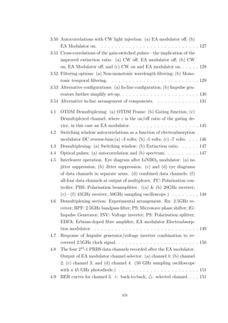
ory [21]. Figure 1.1 graphically illustrates the bandwidth hierarchy of the memory
system (32 MBytes of 16Mbit DRAM) within an admittedly dated 100MHz com-
puter [26]. Most striking is that the bandwidth available within the memory is some
3000 times larger than that provided by the I/O pins—the bottleneck is mostly due
to the pins [27]. The most telling feature is how bandwidth is progressively squan-
dered as hierarchies of elements are crossed within the chip. The net effect is to
increase latency leaving the processor idle for several clock cycles. Moreover mod-
ern computer designs include advanced graphic engines for multimedia rendering
that compete with the processor for a share of the memory bandwidth which makes
matters worse still [28]. Taken together the memory latency, reduced bandwidth and
the faster clock speed serve to conspire against processor efficiency and represent
a large and growing gap between the processor and memory variously termed the
“von Neumann bottleneck” [29] or “memory wall” [30, 31].
However since it is now possible to include additional features and, by implica-
tion, functionality upon a single die a persuasive argument has emerged which con-
tends that if you cannot bring the memory bandwidth to the processor then why not
bring the processor to the memory? This idea for processor-memory integration has
various names: Computational RAM (CRAM) [26]; Intelligent RAM (IRAM) [23];](https://image.slidesharecdn.com/a1b5bb05-a929-4e33-93de-a2dfe5b88eed-160311214335/85/thesis-24-320.jpg)
![Chapter 1 6 Introduction
1TB/s100GB/s10GB/s1GB/s100MB/s
(c) Duncan Elliott 1998, used with permission
Figure 1.1: Typical memory bandwidth hierarchy within a 100MHz computer.
processor-in-memory (PIM) [32]. When implemented it has been conservatively es-
timated that the latency would be reduced by ×10, whilst the bandwidth available
between the memory and the processor would increase ×100 [23]. An additional
benefit that would accrue is that interactions between the PIM and off-chip inter-
connect would be reduced ×100 [33]. In addition a portion of the PIM chip could
be dedicated to re-configurable logic cells so that tailored functionality could be
incorporated after fabrication perhaps dynamically in-situ [32, 34] with attendent
benefits of scale and cost reductions. Once PIM chips become a commercial reality
then multi-PIM computers or networking elements that communicate to neighbour-
ing elements within a cabinet or across a network will emerge. This would shift
the bandwidth and latency bottlenecks onto the interconnection fabric that exists
”outside-the-box” and so low-latency, high bandwidth interconnections to service
this need will be at a premium.
1.2.3 SAN: System Area Networks
Working in the opposite direction it is now widely recognised that many of these
applications can be implemented more cost-effectively using low-cost, networks of
workstations (NOW) [35]. Scalability is possible by just adding more workstations.](https://image.slidesharecdn.com/a1b5bb05-a929-4e33-93de-a2dfe5b88eed-160311214335/85/thesis-25-320.jpg)
![Chapter 1 7 Introduction
Commodity computer clusters are challenging conventional supercomputers in terms
of processing power but for a fraction of the cost. Beowulf from IBM is one working
example that uses conventional LAN technology to interconnect commodity PCs via
standard interface cards connected to the PCI bus4
.
That said the type of problems that can be addressed require a high ratio of
computation-to-communication because of the high latency overhead of conventional
LAN technologies and access via the PCI bus. Consequently problems or applica-
tions that require a low ratio of computation-to-communication are less successful.
To address this deficiency an emerging trend has been to scale-up high-performance
electronic interconnects typical of supercomputers to local-area network (LAN) di-
mensions. These so-called system area networks (SANs) span distances ranging
from 1m-1km—falls between that within a supercomputer cabinet and that of a
LAN [36, 23].
The most commercially successful SAN, to date, is produced by Myricom net-
works. The Myricom approach is centred on an 8-port electronic crossbar-based hub.
Each one of up to 8 hosts is attached to the hub by an electrical cable containing 18
separate twisted pairs (9 in each direction) that allows parallel bi-directional data
transfer of 9-bit words over distances of up to 25m at 1.28Gbit/s (160MByte/s) [37].
Specialised cards interface to the the memory bus within each workstation. The su-
percomputer supernet testbed (SST) envisages internetworking between Myrinet
switches to form a wide area network (WAN) that could interconnect supercom-
puters throughout the west coast of the US [38]. If the Myrinet approach is a
scaling-up of traditional electronic supercomputer fabric. An alternative approach
is to scale-down both developed and emerging technologies in optical networking
which have not been considered applicable over short distances (<1km) [39, 40].
The next section will argue why this alternative approach is now needed.
1.3 Electrical Problems and Optical Solutions
1.3.1 Physical limits of Electrical interconnects
Present-day computers rely on metallic interconnects for chip-chip interconnections.
However the bandwidth that they can provide is now coming up against hard phys-
ical limits. The main constraints include the increase in signal attenuation with
4
17 IBM netfinity servers containing 36 Pentium chips and running the Linux operating system
have equalled the performanace of a $5.5Million Cray T3T-900-AC64 in rendering a ray tracing,
image rendering a ray tracing program. The IBM Beowulf cluster cost only $150,000!](https://image.slidesharecdn.com/a1b5bb05-a929-4e33-93de-a2dfe5b88eed-160311214335/85/thesis-26-320.jpg)
![Chapter 1 8 Introduction
propagation length at frequencies above 1GHz due to the skin-effect resistance of
the metallic track and the nature of the dielectric substrate.
A metric has been proposed based on the aspect ratio–the ratio of propagation
length to cross-sectional area–of cu-based interconnects [41]. This maintains that for
a given length, an interconnect comprising many, small cross-section wires running
at low data rates is equivalent to a few, large cross-section wires running at high data
rates. Traditionally the problem of providing high bandwidth was addressed by the
former approach—spatially multiplexing a flat array of adjacent, parallel metallic
tracks at low signalling frequencies. But as computer clock rates increase so the
adverse effect of capacitative coupling between adjacent tracks leads to enhanced
crosstalk with a consequent loss of data integrity. Data skew between tracks requires
additional de-skewing circuitry and requires careful spatial routing of tracks within
the machine. Consequently there has been a gradual shift away from multiple,
narrow parallel tracks running at 100MHz towards a single serial track operating
at 1+ GHz. The benefits that follow from this approach include the greatly reduced
skew of a single track over several parallel tracks and the relaxation of track routing
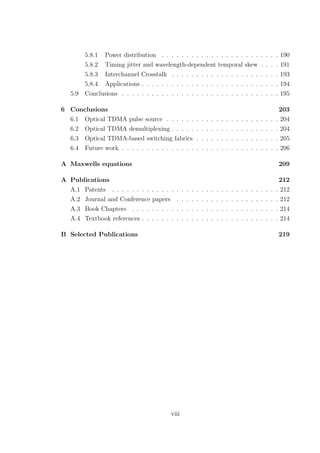
constraints.
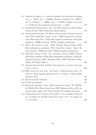
However as clock frequencies increase above 1GHz, the physical limitations inher-
ent in a metallic interconnection network become apparent. Figure 1.2 [42] illustrates
this in graphic form. In effect, each point-to-point link acts as an antenna that
serves as both a source and a sink of time-varying, radio frequency (RF) noise en-
ergy commonly called electromagnetic interference (EMI.) For example, RF noise
energy transmitted to, and received from, the surroundings can affect the decision at
receiver modules and induce phantom data events that cause incoherence between
memory registers. In addition, the fan-out and radiation-induced energy losses need
to be compensated by amplifiers to ensure an adequate signal-to-noise ratio at the
termination points of the system. But the introduction of amplifiers increases noise
and adds to the thermal load and power consumption of the system. Moreover,
thermal variations of the resistance cause variations in the signal phase that require
additional control elements. Nevertheless a pristine, untapped and properly termi-
nated single track with specialised dielectric substrate has been demonstrated to
9.6Gb/s over 0.5m. But this must be qualified by noting that improperly termi-
nated signal taps along the span of the interconnect would adversely impact signal
quality due to reflections from impedance mismatches. Optical Interconnects can
provide a solution to this problem.](https://image.slidesharecdn.com/a1b5bb05-a929-4e33-93de-a2dfe5b88eed-160311214335/85/thesis-27-320.jpg)
![Chapter 1 9 Introduction
10
10
10
10
10
10
13
12
11
9
8
10
10
10
7
6
frequency,Hz
distance, m
Transmission Line
Optics
Wire
1010
-2 -1
1 10
1
10
2
10
3
10
-3
Figure 1.2: Preferred interconnect technology: frequency-distance dependence.
1.3.2 Optical Interconnects emerge
It is easy to appreciate how interconnects have now become the dominant factor
in determining both the productivity and performance of computer technology [43].
Consequently data transfer rates within and between computing machines are sub-
ject to performance bottlenecks that expose the bandwidth limitations of electrical
interconnects and offer a compelling case for optical interconnects.
Amongst the compelling advantages of an opticall interconnect are [44]:
• High distance-bandwidth product: through much lower attenuation and greatly
reduced frequency dependent effects requiring fewer amplifiers.
• EMI immunity providing excellent isolation between data channels.
• High packing density through reduced weight and volume allow greater free-
dom to the system architect.
• Greatly enhanced bandwidth per track through the use of wave-, time-, or
spatial multiplexing can be used to extend the total bandwidth of the fibre](https://image.slidesharecdn.com/a1b5bb05-a929-4e33-93de-a2dfe5b88eed-160311214335/85/thesis-28-320.jpg)
![Chapter 1 10 Introduction
and not be hampered by the limited operational frequency of end-components:
Transmitter modulation and receiver demodulation.
It is this last point that is central to the use of optical fibre, namely the three
bandwidth-enhanced degrees of freedom: spatial, spectral and temporal that can be
provided by optical fibre. For example a number of optical fibres can be assembled
into a spatial multiplex. In turn the wide spectral bandwidth available within each
individual fibre can be utilised for wavelength multiplexing of several distinct data
channels. Each wavelength channel can, in turn, be time-multiplexed in the optical
domain into further independently modulated channels.
A suitable combination of spatial-, wavelength and time-multiplexing can form
a very high capacity interconnect albeit limited by the constraints particular to
each degree of freedom i.e. chromatic dispersion in OTDM system or crosstalk in
a WDM system [?]. For example a range of 16 applied to each dimension gives
an aggregated capacity of over 40Tbit/s (= Modulating frequency of 10GHz x 16
fibres x 16 wavelength channels x 16 time channels.) Of course suitable multiplexing
transmitters and de-multiplexing receivers are required at the access-points of the
system.
But the main constraint to the use of optical interconnects has been down to
economics. Traditionally fibre optic component costs, when compared to their cop-
per brethren, were very much more expensive. Whilst silica optical fibre is cost
comparable to copper, the higher cost of end equipment such as transmitters and
receivers has rendered it viable for all but low-volume, high-margin telecommuni-
cation systems and supercomuters. However this is changing due to the economies
of scale that flow from the mass-production of advanced optical sources such as
distributed feedback (DFB) lasers and high-bandwidth optoelectronic receivers for
deployment in local and wide-area network technologies such as Gigabit Ethernet
and SONET/SDH. Consequently the distance over which optical interconnects com-
bined with advanced switching techniques are becoming economically attractive has
been shrinking continuously [45].
1.3.3 A practical demonstration: Optical Clock Distribu-
tion
Computing machines that contain two or more processors present the software en-
gineer with a concurrent programming environment that considerably lightens the
programming task. This concurrency is ultimately derived from a central clock](https://image.slidesharecdn.com/a1b5bb05-a929-4e33-93de-a2dfe5b88eed-160311214335/85/thesis-29-320.jpg)
![Chapter 1 11 Introduction
source based on a quartz crystal oscillator that generates a global timing reference.
The timing reference is fanned-out and electrically propagated across an interconnec-
tion network comprised of many copper- (or aluminium-) based point-to-point links
that terminate on the spatially dispersed timing modules located on every printed
circuit board, each of which contains one or several processors. The timing module
provides a local timing reference from which the event transitions for the hardware
registers originate. Consequently all local atomic data transition events that occur
within the hardware registers of the processors can be traced to a common source
and hence can be treated as being globally synchronous.
The excess time per clock cycle that remains after each register transition is
referred to as the clock margin. Insufficient clock margin can cause a register to
load or store data either before it has become valid or after it is no longer valid.
Both are manifest as data incoherence between the dispersed registers which if left
unchecked can lead to errors. The clock margin, then, serves to mitigate this effect
by providing timing slack for all global event transitions to occur and settle. But as
machines become physically larger the timing skew arising from the differences in
propagation delay between the dispersed point-to-point links increases and requires
careful design to manage the clock tolerances. These tolerances are now set to
become even tighter as the clock frequency of processors exceeds the 1GHz (sub
1ns) barrier. Moreover the proportion of timing jitter as a fraction of the clock
cycle period becomes more pronounced and places tight constraints on the design
of interconnections between modules.
For these reasons designers of advanced multiprocessor computing machines have
turned their attention towards optical interconnections for clock distribution [46].
Early attempts used free-space optics and weren’t practical propositions because
of the alignment tolerances and mechanical stability as well as clear line-of-sight
optical paths [47] that were required. In this context the benefits of optical fibre
are many. Optical fibre provides a noise-free clock conduit that neither generates
or is affected by RF interference. Its broad bandwidth (tens of THz) can support
high clock transmission rates per optical fibre strand. Silica based optical fibre, in
particular, has extremely low-attenuation and occupies 1/50th the area of a copper
equivalent. It is not constrained by line-of-sight and is mechanically stable
A less well-appreciated advantage of optical interconnects is related to the grow-
ing problem of thermal management and heat dissipation within a modern computer
system [48]. At the microscopic level the increased density of gates on each proces-
sor die adds to the heat flux of the system and this must be serviced at all levels](https://image.slidesharecdn.com/a1b5bb05-a929-4e33-93de-a2dfe5b88eed-160311214335/85/thesis-30-320.jpg)
![Chapter 1 12 Introduction
right up to the cabinet level. Modern multiprocessor systems must remove of the
order 10kW/cm2
of thermal flux. To put this into perspective a thermal flux of
100W/cm2
would be typical one mile from the blast centre of a 1 megaton nuclear
device [49]. At the very least this requires additional cooling elements to remove
the excess generated. To reduce this effect it is necessary to move the processing
elements further apart, in effect trading latency against thermal load. But if the
processing elements are moved apart then the data rate must be reduced because of
the physical limitations such as crosstalk and frequency dependent attenuation of
the Cu-based interconnects that have been outlined earlier.
Somewhat less appreciated is the real-estate constraints that compel manufac-
turers to keep the footprint and overall volume of a system tightly constrained in
line with standardised racking systems. The small cross-sectional area coupled with
its physical flexibility allows optical fibre to make full use of the 3rd dimension to
thread its way through the restricted passages and the confined spaces found within
these machines. The low expansion coefficient and refractive index variation are
particularly compelling reasons for choosing optical fibre. The fast rising edge of
an optical clock distribution system can provide a precise decision point to initi-
ate switching. In fact the viability of the optical approach for clock distribution
has been experimentally demonstrated in the laboratory [50] and found sufficiently
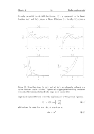
compelling for deployment within a commercial supercomputer system [46]. The
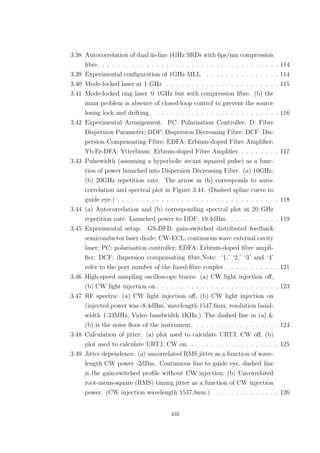
latter is shown in Figure 1.3 where Cray have implemented a laser clock distribu-
tion system for their T90 supercomputer. More recently, Cray have described a
Source: Carol Kleinfield, Cray Research
Figure 1.3: Laser source for clock distribution to module boards within CrayT90
supercomputer.](https://image.slidesharecdn.com/a1b5bb05-a929-4e33-93de-a2dfe5b88eed-160311214335/85/thesis-31-320.jpg)
![Chapter 1 13 Introduction
more advanced, yet potentially lower-cost, version of the clock distribution optics
based on low-cost polyimide waveguides [51].
1.4 Optical data distribution
The next logical step is to extend the use of optics from clock distribution to data
distribution within multi-processor computing systems. Architecturally, clock dis-
tribution is a fanned-out, unidirectional broadcast with a static configuration. In
contrast a data interconnect needs to support bi-directional operation between the
connected nodes. A facility for dynamic reconfiguration that allows any node to
exchange data with any other node is also required. The bandwidth requirements
are substantially higher than for clock distribution and this mandates some form of
multiplexing.
Early attempts at increasing the transmission capacity with optoelectonics used
spatial divivion multiplexing techniques (SDM) utilising multiple fibre ribbon cables.
For example Kaede et al. [52] demonstrated 12×14 Megabit/s in 1990. Since then
research has focussed on low-cost, high-volume versions comprising data-modulated
vertical cavity, surface emitting laser (VCSEL) array transmitters and metal-semiconductor-
metal (MSM) receiver arrays with the interconnection fabric provided by polyimide
ribbon cable. A commercially mature implementation of this technology was devel-
oped during the POLO-2 initiative providing for two contradirectional 10×1Gbit/s
interconnections with an aggregated bandwidth of 20Gbit/s [53].
Yet one single-mode fibre can provide isolation of several independently modu-
lated channels via wavelength division multiplexing. The data transmitted at each
separate wavelength is independent of its neighbours so in effect it forms a virtual rib-
bon cable [54]. All wavelengths are subject to identical environmental effects but do
suffer from deterministic wavelength-dependent data skew. However over extended
distances recent suggestions [55] utilise adaptive electronic bit-skew compensation
and demonstrations [56, 57] have underlined the potential of this approach.
1.5 Shared-media Interconnects
A generic switching fabric is shown in Figure 1.4. Every node contains a transmit-
ter (T) and a receiver (R) to interconvert data between the optical domain within
the fabric and the electrical domain within the attached workstations. In a pho-
tonic packet switching network the route followed by optical packets between the](https://image.slidesharecdn.com/a1b5bb05-a929-4e33-93de-a2dfe5b88eed-160311214335/85/thesis-32-320.jpg)
![Chapter 1 14 Introduction
node1
nodeN
R
T
R
T
R
T
R
T
node3
node2
Photonic
Switching
Fabric
Figure 1.4: Photonic Switching fabric: T: Transmitter; R: Receiver.
source and destination nodes might not be explicitly prescribed. Instead reliance
is placed upon statistical multiplexing which assumes that the bursty nature of the
traffic originating from the nodes after aggregation within the fabric is averaged and
smoothed-out with time. However recent measurements on real networks contradicts
this assumption: traffic aggregation within a network tends to be self-similar on all
time scales and across different length scales from LANs [59] to WANS [60, 61, 62].
Should the aggregated demand for bandwidth exceed that which the fabric can sup-
port then buffering must be provided lest packets be discarded. But buffering can
introduce variable packet latency and out-of-order delivery. Both are undesirable
for real-time multimedia applications such as video.
It would be more useful to establish dedicated connections between nodes across
the photonic fabric and where each connection provides bandwidth in excess of
that generated by, or acceptable to, a node. Now when a connection is established
bandwidth is guaranteed and buffering is unnecessary thus allowing sustained data
transfer without the latency that arises from packet segmentation/reassembly and
buffering—the path between source and destination nodes is explicitly prescribed
and the latency is deterministically defined. However to establish a connection
the underlying network topology becomes critical. It can take several geometric
forms including Bus, Star, Ring, Tree, Mesh, Cubes, Hypercubes [36, 63]. Ideally
the chosen topology should allow connections to be established on-demand and
independently of other traffic within the photonic fabric i.e. be non-blocking.
A shared medium interconnection fabric can allow several nodes to interconnect](https://image.slidesharecdn.com/a1b5bb05-a929-4e33-93de-a2dfe5b88eed-160311214335/85/thesis-33-320.jpg)
![Chapter 1 15 Introduction
independently and concurrently through a sequential assignment of time (or wave-
length) slots, one per node. Data from the write section of a node is time- (or
wavelength-) multiplexed onto the shared optical fibre. The use of tunable time
slot selectors (or wavelength filters) at the receive section of each node allows the
channel of interest to be chosen for reception. The selector must have temporal
(or wavelength) agility to allow synchronisation (in the case of a TDMA network,)
or wavelength stability (within a WDMA network.) Shared medium interconnects
have been usefully classified as [64, 65]
1. Fixed-Transmitter(s), Fixed-Receiver(s) (FT-FR)
2. Tunable-Transmitter(s), Fixed-Receiver(s) (TT-FR)
3. Fixed-Transmitter(s), Tunable-Receiver(s) (FT-TR)
4. Tunable-Transmitter(s), Tunable-Receiver(s) (TT-TR)
The latter two, FT-TR and TT-TR, provide a broadcast and select network where
the transmission from one node can be received by one, many or all other node(s).
The TT-TR approach, though, suffers from an inablilty to broadcast efficiently as
well as the possibility of blocking.
To date most research into single-hop, shared-medium networks has been fo-
cussed on WDM implementations. Examples would include LAMBDANET [66]
from Bellcore which used a FT-FR configuration. Two versions were demonstrated:
18 wavelengths × 1.5 Gbit/s and 16 wavelengths × 2 Gbit/s. At the receive section
of a node the aggregated wavelength channels were spatially separated with each
allocated a separate receiver. The channel of interest was selected electronically.
Rainbow from IBM [67] was a FT-TR network with a broadcast star topology sup-
porting 32 workstations @ 200Mbit/s per wavelength channel. Signaling to effect
channel allocation was distributed to all nodes using a dedicated wavelength channel
that required an additional FT-FR pair within each node. In contrast, there have
been few demonstrations of TDM based interconnects. This is sightly surprising
since clock distribution and recovery is a common requirement of all systems. Barry
et al [68, 69] demonstrated a FT-TR, star-based, implementation that used a non-
linear optical loop mirror (NOLM) for channel gating in a lone receiver. The lack
of additional independent receivers limited the functionality to broadcast-only—bi-
directional transmission was not possible. Bi-directionality is necessary to properly
demonstrate a network. In this thesis the steps that led to the construction of such
a system will be reported.](https://image.slidesharecdn.com/a1b5bb05-a929-4e33-93de-a2dfe5b88eed-160311214335/85/thesis-34-320.jpg)

![Bibliography
[1] J. Bray, “The first telegraph and cable engineers,” in The communications
miracle: The telecommunications pioneers from Morse to the Information Su-
perhighway, ch. 3, pp. 35–47, New York: Plenum Press, 1 ed., 1995.
[2] R. Rapaport, “What does a Nobel prize for radio astronomy have to do with
your telephone?,” Wired Magazine, vol. 3, no. 4, pp. 124–134, April 1995.
[3] J. Bray, “The first telephone engineers,” in The communications miracle: The
telecommunications pioneers from Morse to the Information Superhighway,
ch. 4, pp. 49–59, New York: Plenum Press, 1 ed., 1995.
[4] R. N. Hall, G. E. Fenner, J. D. Kingsley, T. J. Soltys, and R. O. Carlson, “Coher-
ent light emission from GaAs junctions,” Phys. Rev. Lett., vol. 9, pp. 366–368,
Nov. 1 1962. (Received Sept. 24, 1962).
[5] M. I. Nathan, W. P. Dumke, G. Burns, F. H. Dill, and G. Lasher, “Stimu-
lated emission of radiation from GaAs p-n junctions,” Appl. Phys. Lett., vol. 1,
pp. 62–64, Nov. 1 1962. (Received Oct. 6, 1962).
[6] T. M. Quist, R. H. Rediker, R. J. Keyes, W. E. Krag, B. Lax, A. L. McWhorter,
and H. J. Zeiger, “Semiconductor maser of GaAs,” Appl. Phys. Lett., vol. 1,
pp. 91–92, Dec. 1 1962. (Received Oct. 23, 1962, in final form Nov. 5, 1962.).
[7] N. Holonyak and S. F. Bevacqua, “Coherent (visible) light emission from
Ga(As1−xPx junctions,” Appl. Phys. Lett., vol. 1, pp. 82–83, Dec. 15 1962.
(Received Oct. 17, 1962).
[8] C. Kao and E. Hockham, “Dielectric-fibre surface waveguides for optical fre-
quencies,” Proc. IEEE, vol. 113, pp. 1151–1158, July 1966.
17](https://image.slidesharecdn.com/a1b5bb05-a929-4e33-93de-a2dfe5b88eed-160311214335/85/thesis-36-320.jpg)
![Chapter 1 18 BIBLIOGRAPHY
[9] J. Bray, “Optical fiber communication systems,” in The communications mir-
acle: The telecommunications pioneers from Morse to the Information Super-
highway, ch. 17, pp. 269–297, New York: Plenum Press, 1 ed., 1995.
[10] T. Miya, Y. Terenuma, T. Hosaka, and T. Miyashita, “Ultimate low-loss single-
mode fibre at 1.55µm,” Electron. Lett., vol. 15, no. 4, pp. 106–108, February
1979.
[11] R. J. Mears, L. Reekie, S. B. Poole, and D. N. Payne, “Low-noise erbium-doped
fibre amplifier operating at 1.54µm,” Electron. Lett., vol. 23, pp. 1026–1028,
1987.
[12] J. Shurkin, “Eckert and Mauchly,” in Engines of the mind: The evolution of the
computer from mainframes to microprocessors (L. Sonne, ed.), ch. 5, pp. 117–
138, New York: Norton, 1 ed., 1996.
[13] M. Riordan and L. Hoddeson, “Dawn of an age,” in Crystal Fire: The invention
of the transistor and the birth of the information age (E. Barver, ed.), The sloan
technology series, ch. 1, pp. 1–10, New York: Norton, 1 ed., 1997.
[14] M. A. Hiltzik, “Did Xerox blow it?,” in Dealers of Lightning: Xerox Parc and
the Dawn of the Computer Age (L. C. Rowland, ed.), ch. Epilogue, pp. 389–398,
New York: Harper Business, 1 ed., 1999.
[15] K. Hafner and M. Lyon, “A rocket on our hands,” in Where wizards stay up
late: The origins of the Internet, ch. 8, pp. 219–256, New York: Touchstone,
1 ed., 1998.
[16] R. M. Metcalfe and D. R. Boggs, “Ethernet: distributed packet switching for
local computer networks,” Comm. ACM, vol. 19, no. 7, pp. 395–404, July 1976.
[17] H. Frazier and H. Johnson, “Gigabit Ethernet: from 100 to 1,000 Mbps,” IEEE
Internet Computing, vol. 3, no. 1, pp. 24–31, January-February 1999.
[18] How fast is the Internet?, Nov. 1997. http://www.keynote.com/measures/howfast.html.
[19] S. Ortiz, “Hardware-based networking widens the pipes,” IEEE Computer,
vol. 11, no. 5, pp. 8–9, May 1998.
[20] A. Yu, “The future of microprocessors,” IEEE Micro, vol. 16, no. 6, pp. 46–53,
December 1996.](https://image.slidesharecdn.com/a1b5bb05-a929-4e33-93de-a2dfe5b88eed-160311214335/85/thesis-37-320.jpg)
![Chapter 1 19 BIBLIOGRAPHY
[21] F. Baskett and J. L. Hennessy, “Microprocessors: From desktops to supercom-
puters,” Science, vol. 261, no. 5123, pp. 864–871, August 1993.
[22] C. E. Catlett, “In search of Gigabit applications,” IEEE Commun. Mag.,
vol. 30, no. 3, pp. 42–51, April 1992.
[23] D. Patterson, T. Anderson, N. Cardwell, R. Fromm, K. Keeton, C. Kozyrakis,
R. Thomas, and K. Yelick, “A case for intelligent RAM,” IEEE Micro, vol. 17,
no. 2, pp. 34–44, March/April 1997.
[24] J. Backus, “Can programming be liberated from the von Neumann style? a
functional style and its algebra of programs,” Comm. ACM, vol. 21, no. 8,
pp. 613–641, August 1978.
[25] J. R. Goodman, “Using cache memory to reduce processor memory traffic,”
Proc. 10th Annual Int. Symp. on Computer Architecture, pp. 124–131, 1983.
[26] D. Elliott, Computational RAM: A memory-SIMD hybrid. PhD thesis, Depart-
ment of electrical and computer engineering, University of Toronto, August
1998.
[27] D. Burger, J. R. Goodman, and A. K¨agi, “Memory bandwidth limitations of fu-
ture microprocessors,” ACM SIGARCH Computer Architecture News (proceed-
ings of 23rd annual international symposium on Computer architecture (ISCA
’96)), vol. 24, no. 2, pp. 78–89, 22–24 May 1996.
[28] K. Diefendorff and P. K. Dubey, “How multimedia workloads will change pro-
cessor design,” IEEE Computer, vol. 30, no. 9, pp. 43–45, September 1997.
[29] P. G. Emma, “Understanding some simple processor-performance limits,” IBM
Journal Res. Dev., vol. 41, no. 3, pp. 215–232, 1997.
[30] W. A. Wulf and S. A. McKee, “Hitting the memory wall: Implications of the
obvious,” ACM Computer Architecture News, vol. 23, no. 1, pp. 20–24, March
1995.
[31] A. Saulsbury, F. Pong, and A. Nowatzyk, “Missing the memory wall: The
case for processor/memory integration,” ACM SIGARCH Computer Architec-
ture News (proceedings of 23rd annual international symposium on Computer
architecture (ISCA96)), vol. 24, no. 2, pp. 90–101, May 1996.](https://image.slidesharecdn.com/a1b5bb05-a929-4e33-93de-a2dfe5b88eed-160311214335/85/thesis-38-320.jpg)
![Chapter 1 20 BIBLIOGRAPHY
[32] J. B. Brockman and P. M. Kogge, “The case for processing-in-memory,” Com-
puter Science Department Technical Report, no. CSE TR-9707, Jan 10 1990.
[33] D. A. Patterson. Private Communication, 1st December 1998.
[34] D. Culler, J. P. Singh, and A. Gupta, “Future directions,” in Parallel computer
architecture: A hardware/software approach, ch. 12, pp. 935–961, San Francisco:
Morgan Kaufmann, 1 ed., August 1998.
[35] T. E. Anderson, D. E. Culler, and D. A. Patterson, “A case for NOW (networks
of workstations),” IEEE Micro, vol. 15, no. 1, pp. 54–64, February 1995.
[36] J. L. Hennessy and D. A. Patterson, “Interconnection networks,” in Computer
Architecture: A quantitative approach., ch. 7, San Franscisco, CA: Morgan-
Kaufmann, 2 ed., 1996. 562–632.
[37] N. J. Boden, D. Cohen, R. E. Feldermann, A. E. Kulawik, C. L. Seitz, J. N.
Seizovic, and W.-K. Su, “Myrinet: A gigabit-per-second local area network,”
IEEE Network, vol. 15, no. 1, pp. 29–36, February 1995.
[38] L. Kleinrock, M. Gerla, N. Bambos, J. Cong, E. Gafni, L. Bergman, J. Bannis-
ter, S. P. Monacos, T. Bujewski, P.-C. Hu, B. Kannan, B. Kwan, E. Leonardi,
J. Peck, P. Palnati, and S. Walton, “The supercomputer supernet testbed:
A WDM-based supercomputer interconnect,” IEEE J. Lightwave Technol.,
vol. 14, pp. 1388–1399, June 1996.
[39] D. Cotter, M. C. Tatham, J. K. Lucek, M. Shabeer, K. Smith, D. C. Rogers,
D. Nesset, and P. Gunning, “Photonic address-header recognition and self-
routing in ultrafast packet networks,” IEEE/OSA 1996 International Topical
Meeting on Photonics in Switching, 21–25 April 1996.
[40] A. Nowatzyk and P. R. Prucnal, “Are crossbars really dead? The case for opti-
cal multiprocessor interconnect systems,” ACM SIGARCH Computer Architec-
ture News (proceedings of 22nd annual international symposium on Computer
architecture (ISCA95)), no. 23, pp. 106–115, May 1995.
[41] D. A. B. Miller, “Physical reasons for optical interconnections,” Int. J. Opto-
electron., vol. 11, pp. 155–168, 1997.
[42] M. R. Feldman, S. C. Esener, C. C. Guest, and S. H. Lee, “Comparison between
optical and electrical interconnects based on power and speed considerations,”
Appl. Opt., vol. 27, pp. 1742–1751, 1988.](https://image.slidesharecdn.com/a1b5bb05-a929-4e33-93de-a2dfe5b88eed-160311214335/85/thesis-39-320.jpg)
![Chapter 1 21 BIBLIOGRAPHY
[43] J. D. Meindl, “Interconnection limits on 21st century gigascale integration,”
Proc. Mat. Res. Soc. Symp., vol. 514, no. 6, pp. 3–9, 1998.
[44] D. Z. Tzang, “Optical interconnections for digital systems,” IEEE AES Systems
Magazine, vol. 7, no. 9, pp. 10–15, September 1992.
[45] D. Cotter, J. K. Lucek, and D. D. Marcenac, “Ultra-high bit-rate networking:
From the transcontinental backbone to the desktop,” IEEE Commun. Mag.,
vol. 35, pp. 90–95, April 1997.
[46] M. D. Bausman and V. Swanson, “Optical clock distribution system,” US
Patent, no. 5,537,498, Filed March 5, 1993; Assigned July 16, 1996.
[47] W. T. Cathey and B. J. Smith, “High concurrency data bus using arrays of
optical emitters and detectors,” Appl. Opt., vol. 18, no. 10, pp. 1687–1691,
15th May 1979.
[48] H. M. Ozaktas, “Fundamentals of optical interconnections—a review,” Proceed-
ings of the 4th international conference on Massively Parallel Processing using
optical interconnections, pp. 184–189, June 1997.
[49] A. Bar-Cohen, “Thermal management of air- and liquid- multichip modules,”
IEEE Trans. Components, Hybrids, Manuf Technol., vol. CHMT-10, no. 2,
pp. 159–175, June 1987.
[50] P. J. Delfyett, D. H. Hartman, and S. Zuber Ahmad, “Optical clock distribution
using a mode-locked semiconductor laser system,” IEEE J. Lightwave Technol.,
vol. 9, no. 12, pp. 1646–1649, December 1991.
[51] R. T. Chen, L. Wu, F. Li, S. Tang, M. Dubinovsky, J. Qi, J. C. Campbell,
R. Wickman, B. Picor, M. Hibbs-Brenner, J. Bristow, Y. S. Liu, S. Rattanc,
and C. Noddings, “Si CMOS process compatible guided-wave multi-GBit/sec
optical clock distribution system for Cray T-90 supercomputer,” Proc. 4th in-
ternational conference on Massively Paralell processing using optical intercon-
nections (MPPOI ‘97), pp. 10–24, June 1997.
[52] K. Kaede, T. Uji, T. Nagahori, T. Suzaka, T. Torikai, J. Hayashi, I. Watanabe,
M. Itoh, H. Honmou, and M. Shikada, “12-channel parallel optical-fiber trans-
mission using a low-drive current 1.3-µm LED array and a p-i-n PD array,”
IEEE J. Lightwave Technol., vol. LT-8, no. 6, pp. 883–888, June 1990.](https://image.slidesharecdn.com/a1b5bb05-a929-4e33-93de-a2dfe5b88eed-160311214335/85/thesis-40-320.jpg)
![Chapter 1 22 BIBLIOGRAPHY
[53] K. H. Hahn, K. S. Giboney, J. Straznicky, and R. E. Wilson, “Gigabyte-per-
second optical interconnection modules for data communications,” Hewlett-
Packard Journal, vol. 48, no. 5, December 1997.
[54] M. L. Loeb and G. R. Stilwell, “High speed data transmission on an optical
fiber using a byte-wide WDM system,” IEEE J. Lightwave Technol., vol. LT-6,
no. 8, pp. 1306–1311, August 1988.
[55] G. Jeong and J. W. Goodman, “Long-distance parallel data link using
WDM transmission with bit-skew compensation,” IEEE J. Lightwave Technol.,
vol. LT-14, no. 5, pp. 655–660, May 1996.
[56] L. Bergman, J. Morookian, and C. Yeh, “An all-optical long-distance multi-
Gbytes/s bit parallel WDM single-fiber link,” IEEE J. Lightwave Technol.,
vol. LT-16, no. 9, pp. 1577–1582, September 1998.
[57] L. A. Bergman, C. Yeh, and J. Morookian, “Towards the realization of multi-
km × Gbytes/sec bit-parallel WDM single fiber computer links,” Proc. 5th
International Conference on Massively Parallel Processing, vol. IEEE Comput.
Soc., pp. 218–223, June 1998.
[58] K. Tanaka, I. Morita, M. Suzuki, N. Edagawa, and S. Yamamoto, “400Gbit/s
(20×20) dense WDM soliton-based RZ transmission using dispersion flattened
fibre,” Electron. Lett., vol. 34, no. 23, pp. 2257–2258, November 1998.
[59] W. E. Leland, M. S. Taqqu, W. Willinger, and D. V. Wilson, “On the self-
similar nature of ethernet traffic (extended version),” IEEE/ACM Trans. Net-
working, vol. 2, no. 1, pp. 1–15, February 1994.
[60] V. Paxson and S. Floyd, “Wide-area traffic: The failure of poissonian mod-
elling,” IEEE/ACM Trans. Networking, vol. 3, no. 3, pp. 226–244, June 1995.
[61] M. E. Crovella and A. Bestavros, “Self-similarity in world wide web traffic:
Evidence and possible causes,” IEEE/ACM Trans. Networking, vol. 5, no. 6,
pp. 835–846, December 1997.
[62] W. Willinger and V. Paxson, “Where mathematics meets the Internet,” Notices
of the AMS, vol. 45, no. 8, pp. 961–970, September 1998.
[63] D. A. Patterson and J. L. Hennessy, “Parallel processors,” in Computer organi-
zation and design: The hardware software interface, ch. 9, San Franscisco, CA:
Morgan-Kaufmann, 1 ed., 1994. 594–648.](https://image.slidesharecdn.com/a1b5bb05-a929-4e33-93de-a2dfe5b88eed-160311214335/85/thesis-41-320.jpg)
![Chapter 1 23 BIBLIOGRAPHY
[64] B. Mukherjee, “WDM-based local lightwave networks part I : Single-hop sys-
tems,” IEEE Network, vol. 6, no. 3, pp. 12–27, May 1992.
[65] C. Partridge, Gigabit Networking. Reading, Massachusetts: Addison-Wesley,
1st ed., 1994.
[66] M. S. Goodman, H. Kobrinski, V. Vecchi, R. M. Bulley, and J. L. Gimlett,
“The LAMBDANET multiwavelength network: Architecture, applications and
demonstrations,” IEEE J. Sel. Areas Comm., vol. 8, no. 6, pp. 995–1004, Au-
gust 1990.
[67] N. R. Dono, P. E. Green, K. Liu, R. Ramaswami, and F. F. Tong, “A wavelength
division multiple access network for computer communication,” IEEE J. Sel.
Areas Comm., vol. 8, no. 6, pp. 983–984, August 1990.
[68] L. P. Barry, R. F. O’Dowd, J. Debeau, and R. Boittin, “Tunable transform-
limited pulse generation using self-injection locking of an FP laser,” IEEE Pho-
ton. Technol. Lett., vol. 5, no. 10, pp. 1132–1134, October 1993.
[69] L. P. Barry, P. Guignard, J. Debeau, R. Boittin, and M. Bernard, “A high
speed broadcast and select TDMA network using all-optical demultiplexing,”
Proc. ECOC ’95, vol. 1, pp. 437–440, 1995.
[70] J. K. Lucek, P. Gunning, D. G. Moodie, K. Smith, and D. Pitcher, “Syn-
chrolan: A 40Gbit/s optical-TDMA LAN,” Electron Lett., vol. 33, no. 10,
pp. 887–888, 1997.](https://image.slidesharecdn.com/a1b5bb05-a929-4e33-93de-a2dfe5b88eed-160311214335/85/thesis-42-320.jpg)
![Chapter 2
Background material
Claude Shannon described a generalised model of a point-to-point telecommunica-
tions link [1] shown in Figure 2.1. A network is usually composed of many point-
Receiver
Signal Received
Signal
Information
Source Destination
Noise
Source
Message Message
Transmitter
Figure 2.1: Shannon’s generalised communication network.
to-point links since it is uneconomic to establish a dedicated, one-to-one connection
between every user and so rationalisation is desirable to share connections. This
introduces concepts such as multiplexing, routing and switching. These functions
are presently implemented with electronics however research is being undertaken
to implement them optically. The desire is to relegate electronic processing to the
periphery of a network and replacing it with simple, but fast, all-optical techniques
within the network to route and convey information across a room, building, city or
even between continents. The traditional telephone network is circuit switched—a
one-to-one physical path is established between source and destination whether or
not information is being conveyed. But this is now being replaced by packet-switched
24](https://image.slidesharecdn.com/a1b5bb05-a929-4e33-93de-a2dfe5b88eed-160311214335/85/thesis-43-320.jpg)
![Chapter 2 25 Background material
networks based predominantly on the IP protocol. Packet switched networks seg-
ment information into packets that can be aggregated using statistical multiplexing
over many point-to-point links.
Electronics still offers a cost-advantage over optics but it can be anticipated
that this advantage will erode and be supplanted by optics as the demand for high-
bandwidth transmission and switching increases. This trend is reflected in the es-
tablishment of certain bodies such as the optical internetworking forum which sees
router vendors like Cisco, Juniper and Avici sharing the floor with telecommunica-
tions companies like Nortel and Lucent. The Japanese OITDA1
recently produced
a roadmap [2] which outlined the likely evolution of optical networks. Amongst
its forecasts for the year 2010 were: A transmission rate of 100 Mbit/s will be re-
quired within the home; 5 Tbit/s will be required for backbone network systems;
100 Gbit/s for LANs; and 600 Gbit/s for computer backplanes. It is uncertain if
electronics provide this, yet optics certainly can.
2.1 Transmitter
2.1.1 Optical pulse sources
Semiconductor-based devices are the first choice as optical transmitters because they
are compact, consume little power, have no moving parts and are a mature and re-
liable technology. A useful historical review of Semiconductor Lasers is given by
Holonyak [3] in which he credits John Bardeen 2
and his invention of the transistor
as being the starting point. The first theoretical proposition of the use of semicon-
ductors as coherent light sources was derived by John Von Neumann in a note to
Edward Teller in 1953 [4, 5].
During the the autumn of 1962 several groups in the United States demonstrated
stimuated emission from homojunction GaAs [6, 7, 8] and Ga(As1−xPx) [9] material
systems. The devices were essentially forward-biased p-n junctions where above a
critical carrier population (threshold current) population inversion leading to excess
optical gain. A coherent oscillator resulted when a resonant cavity was formed by
cleaving along the natural lattice planes of the material structure. These devices
supported osciilations at several cavity modes each corresponding to a separate wave-
length. Many improvements to the structure of devices was made in the intervening
1
Optoelectronic Industry and Technology Development Association
2
the co-inverntor of the transistor and the only person to win the Nobel prize for Physics
twice—for the Transitor and the BCS theory of superconductivity.](https://image.slidesharecdn.com/a1b5bb05-a929-4e33-93de-a2dfe5b88eed-160311214335/85/thesis-44-320.jpg)
![Chapter 2 26 Background material
years. Most notable was the development of band-gap engineering [3, 10] which
exploited quantum-size effects. The quantum-well3
superlattices that resulted arti-
ficially modified the bulk properties of the materials and produced devices towards
longer wavelengths where optical fibre loss was much lower.
For high speed (≥ 10GHz) TDM-based photonic networks short duration optical
pulses (<10ps) are required at a single wavelength. Data can be imparted onto the
pulses by subsequent external modulation. For semiconductor materials the most
important characteristic of modulation is given by the relaxation frequency, fr. The
bigger, fr, the shorter the pulse duration possible. This is expressed in terms of
some of the fundamental properties of the laser in Equation 2.1 [11],
fr =
1
2π
AP0
τp
(2.1)
where, A, is the differential optical gain; P0, is the average photon density within
the laser cavity; and, τp, is the photon lifetime. There are several techniques of
short optical pulse generation in semiconductor structures. Lau [12] provides a
comprehensive and clear exposition of these techniques in semiconductor lasers, as
do White [13] and Mamyshev [14]. The main techniques are:
1. Mode-locking or phase locking whereby a mechanism within the laser cavity
causes longitudinal cavity modes to interact and become highly correlated.
This process forms a super-modal short optical pulse with a repetition rate
that is inversely proportional to the cavity length. The pulsewidth attainable,
∆τ, is given by Equation 2.2
∆τ =
1
(2M + 1)∆ν
(2.2)
where, ∆ν is the frequency separation between cavity modes; M, is the number
of cavity modes supported within the gain bandwidth of the device. Several
variants of mode-locking are possible. Anecdotally it produces the best pulses
amongst the other varients. However most implementations depend on an
external diffraction grating which can suffer from mechanical instabilities, as
the repetition rate is lowered so the the external cavity must be lengthened:
(a) Active mode-locking: is achieved by actively modulating the gain or loss
of the laser cavity at a frequency equal to the frequency spacing between
3
A quantum-well is formed if a thin slice of a low band gap material, such as InGaAs, is
sandwiched between two layers of a high bandgap material, AlGaAs/GaAs for example.](https://image.slidesharecdn.com/a1b5bb05-a929-4e33-93de-a2dfe5b88eed-160311214335/85/thesis-45-320.jpg)

![Chapter 2 28 Background material
sources (Chapter 3) and de-multiplexers (Chapter 4) will be considered in this
thesis.
2.1.2 External modulation
The techniques described in the last subsection produce an optical pulse sequence
consisting entirely of ‘1’s at the base rate B. External modulation serves to gate
these optical pulses with a time-dependent electrical data signal for transmission
to a remote receiver. In direct detection systems the data is represented by the
presence or absence of light within a time-interval, 1/B.
The electrical field within an optical pulse can be expressed in terms of a time-
dependent vector, E(r, t) given by Equation 2.3 [15]
E(r, t) = E P exp[−ı(k · r − ωct − δ)] (2.3)
where, E is the peak electric field amplitude, P is the polarisation matrix vector, k
is the propagation vector, r is the range vector, ωc is the carrier angular frequency
(≈ 1014
Hz), δ is the carrier phase and t, as usual, represents time. Causality as
represented by the Kramers-Kronig relations [16] dictates that any change in the
imaginary refractive index, nimag, begets a change in the real refractive index, nreal
and vice versa4
. The linewidth-broadening (or linewidth-enhancement) factor, α, is
given by Equation 2.4 [17]
α ≡
∆nreal
∆nimag
(2.4)
where ∆nreal, is the change in the real refractive index inducing a phase change,
and ∆nimag is the change to the imaginary refractive index inducing an absorptive
change.
In an InGaAsP/InP electroabsorption modulator where α is small the application
of a reverse-bias electric field increases the absorption (decreases E in Equation 2.3.)
Consequently the application of a time-varying electrical signal, s(t), opens a time-
varying optical gate or window,
E (1 − mas(t)) P exp[−ı(k · r − ωct − δ)] (2.5)
where ma ≤ 1, is the amplitude modulation index of the device. In contrast, for
LiNBO3, where α is large, the application of an external electical data signal induces
4
Figures 1(a)–(c) of Toll [16] provide a crystal clear exposition and a very intuitive explanation
of the Kramers-Kronig relations based on the principle of classical causality—namely that an event
cannot precede its cause.](https://image.slidesharecdn.com/a1b5bb05-a929-4e33-93de-a2dfe5b88eed-160311214335/85/thesis-47-320.jpg)
![Chapter 2 29 Background material
a change to the refractive index of the material via the Pockels effect. This modulates
the optical path length inducing a phase change to the coherent optical field within
the material. This can be converted to an amplitude change when placed in one (or
both) arms of a Mach-Zehnder interferometer [19]. It can be represented thus
E P exp[−ı(k · r − ωct − δ − mδs(t)] (2.6)
where, mδ, is the phase modulation index of the material and is, ideally, an exact
multiple of π/2 in the balanced Mach-Zehnder geometry described in Chapter 4.
In many cases non-linear effects cause the quantitites in Equation 2.3 to inter-
act. For example, direct electrical modulation of a laser modulates both the the
amplitude and phase of the emitted optical field. The non-monotonic change of the
carrier frequecy is called chirping which leads to power penalties in transmission
systems [20]. Gain-switching which was mentioned in the previous subsection is a
particular variation of direct modulation (the data stream applied is, essentially, a
continuous sequence of ‘1’s.) The, α factor in this case provides a useful index for
the wavelength chirp of the device [17, 18].
2.1.3 Multiplexing
One method that can be used to increase the quantity of information carried between
a source and a remote destination is to increase the data capacity of the intervening
transmission medium. The most obvious technique is to install several more optical
fibres to carry additional, but separate time-division multiplexed systems shown in
Figure 2.1. However the cost of installing more optical fibre may be economically
prohibitive. So in many cases it is preferable to upgrade the transmission and
receiving equipment at both the source and destination of the system, especially
given that a single optical fibre has an estimated 40THz of bandwidth available
in the near-infrared wavelength region. Three techniques are possible: Upgrading
of the TDM link by increasing the transmitter and receiver bit-rates; Wavelength
Division Multiplexing (WDM); Optical Time Division Multiplexing (OTDM).
2.1.3.1 Time-division multiplexing
A typical TDM system is shown in Figure 2.2. Here the optical data rate transmitted
over the optical fibre, the line rate, is equivalent to the electrical signal rate or
base-rate. A high-speed electronic multiplexer (MUX) is required to electrically
combine the data from several information sources (ISn) before application to an](https://image.slidesharecdn.com/a1b5bb05-a929-4e33-93de-a2dfe5b88eed-160311214335/85/thesis-48-320.jpg)
![Chapter 2 30 Background material
IS1
IS2
3
IS
IS
4
4 3 2 1
Tx RxMUX
Key: Optical Path
Electrical Path D
D
D
D4
3
2
1
DEMUX
Signals
Figure 2.2: Typical TDM system.
optoelectronic transmitter (Tx). The current state-of-the-art has been demonstrated
by Siemens over 148km at 40Gbit/s [21]. For bit rates above this recourse to one,
other or both of the two techniques described next is required.
2.1.3.2 Wavelength-division multiplexing
WDM assigns a single TDM channel to an an individual carrier wavelength for trans-
mission. In this way several distinct TDM channels can be carried or multiplexed
across several distinct carrier wavelengths. Figure 2.3 describes how the different
F1
λ4
3λ
λ2
1λ
IS
IS
IS
IS
F2
F3
F4
1λ
λ2
3λ
λ4
λ43λλ21λ
Rx
Rx
Rx
Rx D
D
D
D
Tx
Tx
Tx
Tx
1
2
3
4
1
2
3
4
, , ,
Signals
Figure 2.3: Typical WDM system
channels are distinguished by virtue of wavelength carriers within the optical fibre.
Because the channels are not necessarily at identicaL linerates the system can be
construed as Parallel TDM where each wavelength channel acts as a virtual fibre.
The reverse process, wavelength demultiplexing, occurs at the receiver where band-](https://image.slidesharecdn.com/a1b5bb05-a929-4e33-93de-a2dfe5b88eed-160311214335/85/thesis-49-320.jpg)
![Chapter 2 31 Background material
pass filters or diffractive elements centred on each wavelength carrier channel are
used to isolate each wavelength before it is received.
2.1.3.3 Optical time-division multiplexing
OTDM [22] is again similar to a basic TDM system. However by using temporally
short optical pulses several TDM channels can be interleaved one after the other
as shown in Figure 2.4. The distance between each optical pulse is now, T, so the
12
D
D
4 3
Clock
1
2
3
4
1
2
3
4
CR
Gate
Gate
Gate
Gate
4
3
2
1
D
D
IS
IS
IS
IS
Key: Optical Path
Electrical Path
1
2
3
4
1
2
3
4
Rx
Rx
Rx
Rx
T
2T
3T
4T
T
2T
3T
4T
Tx
Tx
Tx
Tx
Signals
Figure 2.4: Typical OTDM system.
multiplexed transmission rate or line rate is 1/T. At the receiver a clock signal at
the base rate must be recovered to synchronise the de-multiplexing process. This
recovery is typically electronic and current state-of-the-art receivers are performing
this now at 40Gbit/s [23, 24], although all-optical techniques are also possible [25, 26]
and more desirable for OTDM photonic networks because they can form the front-
end of all-optical 3R regenerators [27].
2.2 Optical Transmission
Copper is an excellent conductor. InGaAsP is a representative semiconductor. Glass
is a typical dielectric. These materials are important components for lightwave com-](https://image.slidesharecdn.com/a1b5bb05-a929-4e33-93de-a2dfe5b88eed-160311214335/85/thesis-50-320.jpg)
![Chapter 2 32 Background material
munications at 1550nm. The former is the preferred material for electical transmis-
sion since in copper an applied electic field can cause weakly bound valence electrons
to move from atom to atom—the term often used is an ‘electronic sea’—prompting
an electric current to flow through the conductor. The electronic current that flows
is simply defined by Equation 2.7
J = σjE (2.7)
which is more commonly called Ohms law and where J is the current density, σj is
the jth order conductivity tensor, and E is the electric field vector.
Semiconductors represent a type of behaviour which falls between that of con-
ductors and insulators when subjected to an externally applied electrical field. At
low temperatures semiconductors behave like dielectrics and at higher temperatures
like conductors. Semiconductors can be used in the generation, amplification and
detection of photons.
Conductors, from Ohms law Equation 2.7, have σj = 0. With insulators or
dielectrics valence electrons are more tightly bound to their host atom. The appli-
cation of an electric field now serves to displace or distort the electronic distribution
surrounding the atom giving rise to a separation or polarisation of charge resulting in
a net dipole moment. No current flows, hence σj = 0 ⇒ J = 0 in Equation 2.7. The
relative permitivity, , is used to characterise a dielectric. For glass, the value of is
6. Despite the lack of current flow, energy can be transferred because photons can
be exchanged between the bound electrons. Glass is a good transmission medium
of light energy at the wevelengths that are of interest in lightwave comunications.
Sometimes it is appropriate to consider light as bundles of energy or photons, other
times its better to consider light as an electromagnetic wave [28] when in reality “it
is like neither [29]”. The wave interpretation forms the basis for all electromagnetic
propagation as revealed by the solutions of Maxwells equations under the imposition
of appropriate boundary conditions. The electric displacement vector, D, is defined
as
D = oE + P (2.8)
where o is the electric constant of free space (or vacuum permitivity) equal to
8.85 × 10⁻¹²
farads/meter. E is the electric field vector and P is the polarization
vector. The electrical susceptibility tensor of order j, χ(j)
, relates P and E thus
Pi = oχ
(1)
ij Ej (2.9)
when a linear, isotropic material is assumed. This will allow us to to set the higher
order terms (j > 1) to zero and replace χ(1)
by χ . This simplifies the expression for](https://image.slidesharecdn.com/a1b5bb05-a929-4e33-93de-a2dfe5b88eed-160311214335/85/thesis-51-320.jpg)
![Chapter 2 33 Background material
Equation 2.8 to
D = o E (2.10)
where is the relative permitivity and is equivalent to 1 + χ. It is also possible to
relate the magnetic field, B to the magnetizing field, H and the magnetization, M
thus
B = µo(H + M). (2.11)
The constant, µo, is the magnetic constant of free space (or vacuum permeability)
and it is equal to 4π×10−7
henrys/meter. By introducing the magnetic susceptibility,
χm we arrive at the magnetic analogue of Equation 2.10
B = µo(1 + χm )H = µoµH. (2.12)
This approach is further developed for the cylindrical geometry of a typical single-
mode optical fibre in Appendix A.
2.2.1 Single-mode optical fibre
The approach presented in Appendix A was well understood iny 1966 when Kao
and Hockham wrote in their seminal paper [31], which ushered in the fibre optics
revolution:
A dielectric fibre with a refractive index higher than its surrounding region
is a form of dielectric waveguide which represents a possible medium for the
transmision of energy at optical frequencies.
Kao and Hockham also recognised that the HE11 mode or single-mode condition was
of particular interest. They outlined the various loss mechanisms, to be described in
subsequent sections, including Rayleigh scattering and material absorption. They
identified that the crucial material problem was to reduce the loss figure to around
20db/km. (At that time the figure was typically 1000db/km for fused silica glass.)
By 1970 Corning had produced 20db/km fibre which immediately started a flurry
of interest in the use of fused-silica fibre as a transmission medium [32].
The simplest, single-mode, optical fibre is a dielectic waveguide of circular cross
section consisting of a central core of radius, a, with a refractive index, ncore, enclosed
within a concentric cladding with a refractive index of, nclad and outer diameter,
b. If ncore > nclad then light of wavelength, λ0 is trapped or guided provided the
normalised frequency, V , satisfies the equality given by Equation 2.13
V =
2πa
λ0
n2
core − n2
clad < 2.405 (2.13)](https://image.slidesharecdn.com/a1b5bb05-a929-4e33-93de-a2dfe5b88eed-160311214335/85/thesis-52-320.jpg)
![Chapter 2 35 Background material
where, w, represents the gaussian spot size. Marcuse [33] gave the empirical formula
given by Equation 2.16
w = a 0.65 +
1.619
V 1.5
+
2.879
V 6
. (2.16)
for, w, in a single-mode optical fibre, This allows the light intensity of the funda-
mental mode to be estimated simply by dividing the optical power, P, by, Aeff.
2.2.2 Optical fibre attenuation
The Silica-based glass-fibre used in optical communication systems is, with suitable
qualification, transparent within the spectral range from 800—1600nm as can be
seen in Figure 2.6 [34]. Since 1970 three telecommuncations windows have been
Figure 2.6: Typical Attenuation vs. Wavelength response of a Germania-doped
Silica optical fibre. (Data provided by D. L. Williams, BT Laboratories.)
used for transmission: 850nm, 1300nm and 1550nm. Utilisation of each window
depended on the device technology availaile at the time. The lowest attenuation
can be found at 1550nm where values of 0.2dB/km are common.
Ultraviolet and infrared absorption scattering due to atomic resonances in sil-
ica account for intrinsic losses. The infrared scattering becomes pronounced for
wavelengths beyond 1600nm, the so called IR-band edge. The main extrinsic loss
mechanism is due to harmonics of the Si-O resonance centred at 2800nm, with over-
tones at 950nm and 1370nm. Moisture ingress during manufacture, installation or](https://image.slidesharecdn.com/a1b5bb05-a929-4e33-93de-a2dfe5b88eed-160311214335/85/thesis-54-320.jpg)
![Chapter 2 36 Background material
during the lifetime of the fibre combines with the Si-O resonance giving rise to com-
bination structures at 880nm and 1230nm [32]. Nevertheless careful monitoring of
the environent during the fibre pulling process and installation has all but elimi-
nated this. Microscopic variations of the glass density give rise to the remaining loss
mechanism—Rayleigh scattering. This serves to convert guided photons to radiative
photons and is represented by Equation 2.17
αR = CR
1
λ4
[dB/km] (2.17)
Where αR is the loss in dB/km, CR is the Rayleigh scattering coefficient, and λ
is the wavelength. The influence of all these loss mechanisms means that power
launched into an optical fibre attenuates as it propagates. Equation 2.18
P(L) = P(0) exp(−αL) (2.18)
where, P(0), is the launched power; P(L) is the attenuated power after propagating
a distance, L. The attenuation coefficient, α, is usually expressed in terms of dB/km,
as
αdB = −
10
L
log10
P(L)
P(0)
(2.19)
and it is convenient to define an effective length, Leff, over which the power drops
by a factor of 1/e, as follows,
Leff =
1 − exp−αL
α
(2.20)
2.2.3 Optical fibre dispersion
In a normally dispersive optical fibre short wavelengths (higher frequencies) travel
more slowly than long wavelengths (lower frequencies.) For an an anomalously dis-
persive fibre the reverse holds. As a result optical pulses of finite spectral width
launched into an optical fibre tend to change their temporal width during propa-
gation because of their finite spectral width. This is linear dispersion. A useful
analogy might employ the visual spectrum where blue light has a shorter wave-
length than red light. After propagation in a normally dispersive optical fibre long
wavelength (“red”) components would move towards the leading edge of an optical
pulse, whereas the short wavelength (“blue”) components would fallback towards
the trailing edge. It is useful to describe these frequency dependent effects in terms
of the mode propagation constant of the fibre, β(ω), which can be usefully expressed
as a Taylor series expansion about the centre frequency, ω0, thus
β(ω) = β0(ω) + β1(ω − ω0) +
1
2
β2(ω − ω0)2
+ · · · (2.21)](https://image.slidesharecdn.com/a1b5bb05-a929-4e33-93de-a2dfe5b88eed-160311214335/85/thesis-55-320.jpg)
![Chapter 2 37 Background material
where the taylor coefficients are given by,
βm =
dm
β
dωm
ω=ω0
(2.22)
The first two coefficients,
β1 =
1
c
n + ω
dn
dω
=
ngroup
c
=
1
vgroup
(2.23)
β2 =
1
c
2
dn
dω
+ ω
d2
n
dω2
=
λ3
2πc2
d2
n
dλ2
(2.24)
are of particular significance: β1 is related to the group velocity of the pulse, vgroup,
which indicates the speed of the pulse within the fibre; whilst β2, the Group Velocity
Dispersion (GVD) parameter, indicates how the pulse broadens with propagation.
Its dimensions are ps2
/nm. Dispersion for an optical fibre is usually expressed in
terms of the Group Delay Dispersion (also called the Total Dispersion), D,
D =
dβ1
dλ
= −
2πc
λ2
β2 (2.25)
It is important to note the presence of the minus sign ‘-’ in Equation 2.25 and that
it is expressed dimensionally as ps/nm/km or ps/nm-km. The group delay disper-
sion is a very useful parameter in optical fibre transmission because it relates the
spectral width, temporal width and propagation distance of the fibre together. Ta-
ble 2.1 summarises the above. In standard fibre (SF) the minimum dispersion occurs
Fibre type Leading edge GVD Group Delay Disp.
[β2 (ps2
/nm)] [D (ps/nm/km)]
Normal red positive (> 0) negative (< 0)
Anomalous blue negative (< 0) positive (> 0)
Table 2.1: Classification and properties of normal and anomalously dispersive optical
fibre.
at ∼1300nm shown in Figure 2.7(a) [35]. Standard fibre is normally dispersive for
wavelengths <1300nm and anomalously dispersive for wavelengths >1300nm. In
dispersion shifted fibre (DSF) the dispersion minimum is shifted out to ∼1550nm
where attenuation is minimised. Representative dispersion versus wavelength char-
acteristics are depicted in Figure 2.7(b). To understand how the dispersion can
be tailored it is necessary to consider the two main mechanisms: Material and
Waveguide dispersion, and how the latter can be controlled to shift the dispersion
minimum.](https://image.slidesharecdn.com/a1b5bb05-a929-4e33-93de-a2dfe5b88eed-160311214335/85/thesis-56-320.jpg)
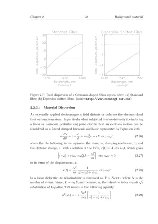
![Chapter 2 39 Background material
In an inhomogenous material system such as a Silica:Germania-based optical fibre
the contributions of non-identical atoms must be accounted for by a weighting factor,
fj, where fj = 1
n2
(ωc) = 1 +
Ne2
m 0 j
fj
ω2
0j − ω2
c + ıγωc
(2.30)
When Equation 2.30 is expressed in terms of wavelength, λ, then it is commonly
called the Sellmeier equation. This describes the dependence of the refractive in-
dex, n, on the externally applied electromagnetic field characterised by its carrier
wavelength, λc.
n2
(λc) = 1 +
m
j=1
Bjλc
λ2
c − λ2
0j
(2.31)
For fused bulk-silica the following values are given: B1 = 0.6961663, B2 = 0.4079426,
B3 = 0.8974794, λ1 = 0.0684043µm, λ2 = 0.1162414µm and λ3 = 9.896161µm [36].
When subjected to a high-intensity (i.e inducing a non-linear or anharmonic pertur-
bation) plane electric field it is appropriate to consider a forced damped anharmonic
(or non-linear) oscillator model which results in additional nonlinear terms. These
extra terms induce additional electric fields and self-action effects which are the
realm of nonlinear optics [37]. Some of these nonlinear optical effects will be con-
sidered later in this chapter.
2.2.3.2 Waveguide Dispersion
Waveguide dispersion arises from the different mode propagation constants, β, of
an electromagnetic field in the core and cladding of an optical fibre. Whilst the
material dispersion is fundamentally linked to the material composition of the fibre
and is controlled by the material composition of the fibre, the waveguide dispersion
is linked to the geometrical design of the fibre, or more particularly the refractive
index profile. This can be modified by design. The total dispersion, D, then is the
numerical sum of both the material and waveguide dispersion values, Equation 2.32,
D = Dmaterial + Dwaveguide. (2.32)
It is useful to consider the mode confinement factor, Γ(λ), which expresses the
proportion of optical power within the core of an optical fibre and is given by Equa-
tion 2.33,
Γ(λ) =
a
0 rE2
(r, λ)dr
∞
0 rE2(r, λ)dr
(2.33)](https://image.slidesharecdn.com/a1b5bb05-a929-4e33-93de-a2dfe5b88eed-160311214335/85/thesis-58-320.jpg)
![Chapter 2 40 Background material
For example if Γ(λ) = 1 then all the optical power is contained within the fibre
core and the waveguide dispersion would be that of the core alone. Alternatively
if Γ(λ) = 0 then all the optical power is contained in the cladding and the waveg-
uide dispersion is that of the cladding 5
. In practice the power of a guided mode is
distributed between the core and the cladding. So manipulation of the power distri-
bution between the core and cladding, by appropriate design, changes the waveguide
dispersion which, in turn, can tailor the total dispersion. This is the method that
is used to shift the dispersion zero from 1300nm to 1550nm in a dispersion-shifted
fibre (see Figure 2.7(b)).
2.2.3.3 Dispersive propagation and wavelength chirp
In a linear, isotropic optical fibre, change their temporal pulsewidth with propa-
gation. This can be appreciated by considering the effect of chromatic dispersion
on the electric field of an optical pulse represented by U(ξ, τ), subject to Equa-
tion 2.34 [38, 39]
−i
∂U
∂ξ
= ±β2
1
2
∂2
U
∂τ2
+ iΓU. (2.34)
that describes the propagation of an optical pulse in a lossy, optical fibre, where the
various normalising terms are defined as follows,
τ =
t − β1z
T0
, ξ =
z
LD
, U =
A
Ppeak
, Γ =
α
2
LD, (2.35)
where, τ, is the normalised time; ξ, is the normalised distance; LD, is a dispersion
length; A, represents the amplitude envelope of the electric field that comprises the
optical pulse; and α is a loss term in units of inverse length. At this point it is
useful to recall some of the theory of fourier transforms namely that the following
expressions hold when U(ξ, τ) and ˜U(ξ, ω) are fourier transform pairs,
U(ξ, τ) =
1
√
2π
+∞
−∞
˜U(ξ, ω)e−ιωτ
dω ⇐⇒ ˜U(ξ, ω) =
1
√
2π
+∞
−∞
U(ξ, τ)e+ιωτ
dτ,
(2.36)
from the properties of fourier transforms it follows that,
∂U(ξ, τ)
∂τ
=
1
√
2π
+∞
−∞
−ιω ˜U(ξ, ω)e−ιωτ
dω = −ιω ˜U(ξ, ω), (2.37)
and in addition,
∂2
U(ξ, τ)
∂τ2
= −ω2 ˜U(ξ, ω). (2.38)
5
Of course both cases are physically unrealisible since neither would support a guided mode
within the fibre due to spatial diffraction.](https://image.slidesharecdn.com/a1b5bb05-a929-4e33-93de-a2dfe5b88eed-160311214335/85/thesis-59-320.jpg)
![Chapter 2 41 Background material
Now to simplify Equation 2.34 assume that the single-mode optical fibre is lossless
i.e. α ⇒ Γ = 0 then,
i
∂U
∂ξ
= β2
1
2
∂2
U
∂τ2
. (2.39)
using the RHS of Equation 2.38 This can be rewritten using the RHS of Equa-
tion 2.38 as,
i
∂ ˜U
∂ξ
= ±
β2
2
ω2 ˜U(ξ, ω) (2.40)
which is the equation for simple harmonic motion with one solution being,
˜U(ξ, ω) = ˜U(0, ω) exp +i
β2ω2
ξ
2
. (2.41)
This confirms that in the frequency domain no new frequency components are pro-
duced during propagation. Now because the pulse has a finite wavelength spread
then dispersion will occur in the time domain because the different wavelength com-
ponents will travel with different velocities. Consider an initial gaussian pulse enve-
lope6
described in the time and frequency domain by Equation 2.42
U(0, τ) = exp −
τ2
2σ2
o
⇐⇒ ˜U(0, ω) = 2πσ2
o exp −
ω2
σ2
o
2
. (2.42)
To simulate the effect of propagation recall Equation 2.36 but where ˜U(ξ, ω) is
replaced by Equation 2.41 to give Equation 2.43
U(ξ, τ) =
1
√
2π
+∞
−∞
˜U(0, ω) exp −i
β2ω2
ξ
2
exp (−ιωτ) dω, (2.43)
All that needs to be done now is to substitute Equation 2.42 to give Equation 2.44,
U(ξ, τ) = σo
+∞
−∞
exp −
ω2
2
(σ2
o − iβ2ξ) . exp (−ιωτ) dω (2.44)
where use was made of the definite integral given by Equation 2.45
+∞
−∞
exp (−p2
x2
± qx) dx =
√
π
p
exp
q2
4p2
, p > 0. (2.45)
found in mathematical tables [40]. Also in Equation 2.44, U(ξ, τ) was given by
Equation 2.46,
U(ξ, τ) =
σo
σ2
o − iβ2ξ
exp −
τ2
2(σ2
o − iβ2ξ)
(2.46)
6
Note that it follows for Equation 2.42 that the input intensity in is, |U(0, τ)|2
= exp −τ2
σ2
o
.
The Intensity, I, can be written as Equation 2.69 in the time domain](https://image.slidesharecdn.com/a1b5bb05-a929-4e33-93de-a2dfe5b88eed-160311214335/85/thesis-60-320.jpg)
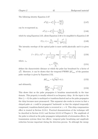
![Chapter 2 43 Background material
within each pulse is conserved. If a sequence of optical pulses are launched into an
optical fibre then the individual energy of each pulse can spill into adjacent time-slots
such that the data, after detection, contains an increased number of errors [41].
2.2.3.4 Linearly chirped pulse compression analysis
As we shall see in Section 3.3.3 of Chapter 3 the optical pulses generated by a
gain-switched DFB laser have the high-frequency or “blue” components at the front
of the pulse. The wavelength components then smear-out (or chirp) into the low-
frequency “red” components located at the back of the pulse. A normally dispersive
fibre (β2 > 0) can be used to delay the blue components with respect to the red
components so that, after a certain optimum distance, the red and blue compo-
nents coincide temporally, which corresponds to the transform-limited, minimum
pulsewidth. It follows that propagation beyond the optimum distance will result
in pulse broadening because the red components, “pass-through,” and eventually
leave, the blue components in their wake. It is useful to extend the analysis from
the last Section by once again considering a lossless, linear and isotropic optical fibre
but where the input gaussian pulse now has an initial wavelength chirp. In this case
the electric field can be represented by Equation 2.54,
U(0, τ) = exp −(1 + ıC)
τ2
2σ2
o
⇐⇒ ˜U(0, ω) =
2πσ2
0
1 + ıC
exp −
ω2
σ2
0
2(1 + ıC)
(2.54)
where C is a linear chirp parameter that can take positive or negative values; and σ0,
is the 1/e pulsewidth, such that σ0 = ∆Tfwhm
/2
√
ln 2, ∆Tfwhm
being the full-width
half-maximum pulsewidth. When the LHS of Equation 2.54 is applied to the pulse
propagation equation Equation 2.34, then Equation 2.55 is obtained,
U(ξ, τ) =
σ0
σ2
0 − ıβ2 (1 + ıC)
exp −
(1 + ıC)τ2
2 [σ2
0 − ıβ2ξ(1 + ıC)]
. (2.55)
As before, a Fourier transform of Equation 2.55 into the time domain gives, Equa-
tion 2.56
I ∼ |U(z, τ)|2
=
1
1 + C z
zo
2
+ z
zo
2
exp
−
τ2
σ2
o 1 + C z
zo
2
+ z
zo
2
(2.56)
where Equation 2.51 has been used. It is now possible to obtain the analogous
expression to Equation 2.52 for the temporal pulse broadening in the presence of
linear chirp.
∆Tout
∆Tin
= 1 + C
z
zo
2
+
z
zo
2
(2.57)](https://image.slidesharecdn.com/a1b5bb05-a929-4e33-93de-a2dfe5b88eed-160311214335/85/thesis-62-320.jpg)

![Chapter 2 45 Background material
to recover a linear state prior to insertion into the polarisation-dependent compo-
nent. An alternative technique is to deliberately induce a large birefringence into
the fibre during manufacture [42]. This defines two orthogonal polarisation axes
within the fibre where a linear state will be maintained during transmission. Such
fibre is classed as polarisation-maintaining (PM.) In practice crosstalk between the
polarisation states occurs. This is defined as, δXT, the crosstalk ratio,
δXT = 10 log10
Py
Px
(2.61)
where Px and Py are the powers at the output of the fibre of the HEx and HEy modes
assuming that the linear state at the input was launched exclusively into the HEx
mode. The PANDA fibre used in the first version of SynchroLan to be described
later in this thesis in Section 5.3 of Chapter 5 had a crosstalk of ∼27dB after 5km
at 1560nm [42]. Additional crosstalk creeps in due to the splicing process despite
the use of specialised fusion splicers.
2.2.5 Non-linear effects
When the magnitude of the optical field that acts upon the bound electrons within
a silica-based optical fibre is large their motion can be approximated to that of an
anharmonic oscillator. This may be expressed as a power series expansion of the
polarisation vector, P, such that Equation 2.9 can be re-expressed as Equation 2.62
Pi = o(χ
(1)
ij Ej + χ
(2)
ijkEjEk + χ
(3)
ijklEjEkEl + · · ·) (2.62)
where χ(n)
is the nth
-order susceptibility tensor. For a centrosymmetric, isotropic
medium such as a silica optical fibre with inversion symmetry χ
(n)
ijk··· = 0 when n is
even. Of the odd terms (n = 3, 5, 7, . . .) that remain the most important is the third
order susceptibility tensor, χ
(3)
ijkl. Although this tensor has 81 components it can be
simplified by symmetry arguments. Firstly, fields and terms along the direction of
propagation (z-direction) can be neglected because only orthogonally polarised light
(x- and y-directions) is considered during propagation. Secondly, if we assume that
the electric field is linearly polarised along the x-axis we can write χ
(3)
ijkl = χ3 . (A
comprehensive exposition of these arguments is beyond the scope of this thesis, but
explicit details can be found in [43].) Consequently the third-order polarisation can
be written as Equation 2.63,
Px = 0 χ3 E3
x . (2.63)](https://image.slidesharecdn.com/a1b5bb05-a929-4e33-93de-a2dfe5b88eed-160311214335/85/thesis-64-320.jpg)
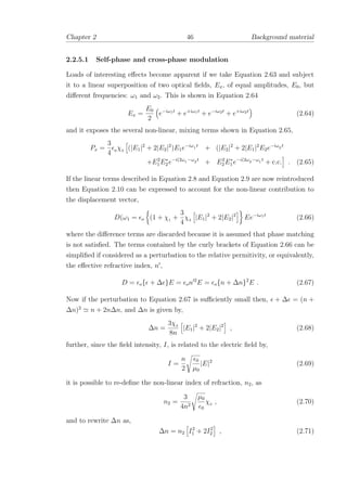

![Chapter 2 48 Background material
elements the soliton can be maintained indefinitely [44]. The non-linear Schr¨odinger
(NLS) equation Equation 2.74 [45, 46],
−i
∂U
∂ξ
= ±β2
1
2
∂2
U
∂τ2
+ iΓU + N2
|U|2
U. (2.74)
can be used to model these effects, however its explicit derivation is beyond the scope
of this thesis. The various normalising terms shown in Equation 2.74 were already
defined in Equation 2.35. In fact, the NLS equation is identical to that used for
linear pulse propagation pulse propagation , Equation 2.34, but for the addition of
the N2
|U|2
U term that is dependent on the intensity of the electric field, |U|2
, which
is none other than the Kerr effect defined earlier by Equation 4.4. The solution of
Equation 2.74 obtained for Γ = 0 and with the second-term of Equation 2.74 positive
is,
U(ξ, τ) = N2
e(iξ
2 sech(τ) (2.75)
which describes the fundamental soliton that propagates without change of shape
(although the phase of the electric field does evolve.) The peak power of the funda-
mental soliton is given by Equation 2.76
Ppeak = 0.777 N2 λ3
π2cn2
|D|
τ2
Aeff, (2.76)
where all the terms have been defined earlier. For the particular cases where N = 1
any increase to the peak power results in a more complex evolution of the temporal
and spectral properties of the pulse during propagation. The soliton period, z0, is
defined by Equation 2.77
z0 =
π
2
LD = 0.322
2πc
λ2
Tfwhm
D
, (2.77)
which represents the propagation distance over which a higher-order soliton (N ≥ 2,
with N an integer) recovers its initial profile [47].
The loss accumulated during propagation reduces the effectiveness of SPM until
eventually the dynamic balance with GVD is lost and the pulse broadens. Judicious
placement of discrete or distributed gain elements along the propagation path serves
to restore SPM and by implication the soliton. Ellis et al. [48] assert that the
amplifier spacing, Lamp, for an N = 1 soliton in terms of the soliton period should
be,
Lamp <
z0
6
(2.78)
to ensure the fidelity of the soliton. Moreover if adiabatic gain, in excess of the loss,
is provided, SPM dominates and additional temporal pulse compression is possible.](https://image.slidesharecdn.com/a1b5bb05-a929-4e33-93de-a2dfe5b88eed-160311214335/85/thesis-67-320.jpg)
![Chapter 2 49 Background material
This will be explored in the Section 3.3.4 of Chapter 3 as a means to obtain non-
linear pulse compression of short optical pulses.
2.2.6 Amplification
The optical power detected at the termination of a transmission link must be above
the sensitivity of the optoelectronic detector to ensure reliable data reception. A
lossless optical fibre would allow an infinite transmission length provided dispersive
pulse-broadening could be controlled. However optical fibre is lossy and this reduces
the link length. By compensating for this loss, optical amplifiers can be used to
extend the span of the transmission system. In optical amplifiers (and lasers) a
pump source is used to invert the equilibrium population distribution between two
or more energy levels of a material. Whereas a laser is a lossy resonator which
acts to ‘trap’ photons into making several circulations of the cavity before emission,
a travelling wave amplifier is constructed to suppress resonance effects. Amplified
photons pass through the cavity once and without recirculation. Inevitably there is
a finite number of spontaneous photons which induce stimulated emission and are
amplified. This amplified spontaneous emission (ASE) if uncontrolled can limit the
number of amplifiers that can be concatenated.
More formally an amplifier provides gain, G, so that the optical power that
emerges from the amplifier output stage, Pout, is greater than that presented at the
input, Pin,
G =
Pout
Pin
. (2.79)
The amount of gain that can be provided is finite and as Pin is increased the amplifier
becomes saturated and the gain, G, begins to decrease. This is represented by
Equation 2.80 [49]
G = G0 exp −
G − 1
G
Pout
Psat
(2.80)
where Psat represents the saturated optical power and G0 is the unsaturated gain
describes the gain compression that occurs as Pout → Psat.
2.2.6.1 Noise and spontaneous emission
Amplifiers add noise which degrades the signal-to-noise ratio (SNR.) The noise fig-
ure, F,
F =
SNRin
SNRout
(2.81)](https://image.slidesharecdn.com/a1b5bb05-a929-4e33-93de-a2dfe5b88eed-160311214335/85/thesis-68-320.jpg)
![Chapter 2 50 Background material
is a useful indicator of this degradation. For a set of n concatenated amplifiers the
effective noise figure, Fn [49], is given by
Fn = F1 +
F2
G1
+
F3
G1G2
+ · · · +
Fn
n
1 Gn
(2.82)
which prescribes that the amplifier with the highest gain and lowest noise figure
should appear first, with the succeeding amplifier having the next highest gain and
lowest noise figure and so on. If a very simple two-level system is considered where
the ground state has N1 atoms and the excited state has N2 atoms then a sponta-
neous emission factor, nsp, can be defined as
nsp =
N2
N2 − N1
. (2.83)
The spontaneous emission factor can be related to the noise figure,
Fn = 2nsp
G − 1
G
(≈ 2nsp, for G 1) (2.84)
so that even for the ideal situation of full inversion (nsp = 1) the noise figure is at
least 3dB.
Amongst the many desirable attributes that an optical amplifier should possess
are: high gain; high saturation power; a wide, flat and low-ripple gain bandwidth;
polarisation insensitivity; low ASE noise; tolerance to bit-patterning; bit-rate trans-
parency; low channel crosstalk (for WDM systems); low end-to-end coupling loss;
use within the second (∼1300nm) or third (∼1550nm) wavelength regions [50]. This
latter attribute arises because deployed optical fibre transmission systems operate
at either 1300nm (the dispersion minimum for standard fibre) or 1550nm (the loss
minimum for optical fibre.) Less seldom mentioned is reliability and robustness
since real transmission systems are often housed in inhospitable environments with
poor accessibility. There are three main positions where amplifiers can be placed
within a transmission system. If located immediately after the transmitter they are
considered as power amplifiers serving to increase the launched power which trans-
lates into an extension of the link length. If placed at the end of the transmission
link then they can be used as receiver pre-amplifiers to improve the signal-to-noise
ratio at the detector. An advantage of having the amplification at either end of the
transmission link arises from the ease of access and management. In long fibre spans
in-line amplifiers periodically regenerate attenuated signals. But should the useful
signal presented to the input of an optical amplifier be too weak, then ASE can sat-
urate the amplified output signal. Consequently ASE build-up limits the number of](https://image.slidesharecdn.com/a1b5bb05-a929-4e33-93de-a2dfe5b88eed-160311214335/85/thesis-69-320.jpg)
![Chapter 2 51 Background material
amplifiers that can be cascaded which constrains the maximum transmission length
before ‘3R’ regeneration is required.8
This is a consequence of the analogue nature
of the amplifying process. Two mature candidates have emerged as the optical am-
plifier of choice in deployed optical fibre links. The first is the electically-pumped
travelling wave semiconductor optical amplifier (TWSOA) [51]; the second is the
optically-pumped erbium-doped optical fibre amplifier (EDFA [52].)
2.2.6.2 Travelling wave semiconductor optical amplifiers
TWSOAs are based on mature laser diode technology. Yet they are not lasers since
they operate below threshold aided by angled end-facets and with anti-reflection
coatings to prevent resonances so ensuring a wide, flattened and low-ripple 3dB
gain band of ∼50nm. They can be fabricated for operation at either 1300nm or
1550nm. Although they can operate bi-directionally it is usual to splice optical iso-
lators appropriately to the input and output pigtails to prevent reflections. This
renders them unidirectional. Most troublesome is the polarisation sensitivity due
to the single pass gain being different for TE and TM modes because the optical
confinement factors differ i.e. ΓTM = ΓTE [51]. This necessitates either active po-
larisation control or polarisation scrambling in a real system. A key feature which
affects the performance of TWSOAs is the repopulation time of the upper energy
level of the amplifier transition. The spontaneous lifetime of this metastable level
is ∼100–500ps. Should the interpulse separation approach that of the spontaneous
lifetime of a saturated amplifier the gain (and optical phase) fluctuates in response
to the preceeding bit-pattern history. This affects the amount of gain available to
subsequent pulses and is manifest as patterning in a single-wavelength system or
crosstalk in WDM systems at gigabit rates. Phase modulation (or chirp) is unde-
sirable in transmission systems however it can be very usefully exploited to perform
all-optical switching functions using TWSOAs incorporated within interferometric
devices. This will be treated in more detail in Section 4.3.1.3 of Chapter 4.
2.2.6.3 Erbium-doped fibre amplifiers
The move to 1.55µm optical transmission systems was made possible by the rapid
development of the EDFA during the latter part of the 1980s and the early 1990s.
Being an in-fibre component EDFAs are easily connected or spliced (ensuring min-
imal coupling loss) to deployed fibre to provide a ∼30nm wide gain bandwidth as
8
‘1R’ is the Regenerative property of an optical amplifier, ‘2R’refers to Regenerate and Reshape,
whilst ‘3R’ means Regenerate, Reshape and Retime.](https://image.slidesharecdn.com/a1b5bb05-a929-4e33-93de-a2dfe5b88eed-160311214335/85/thesis-70-320.jpg)
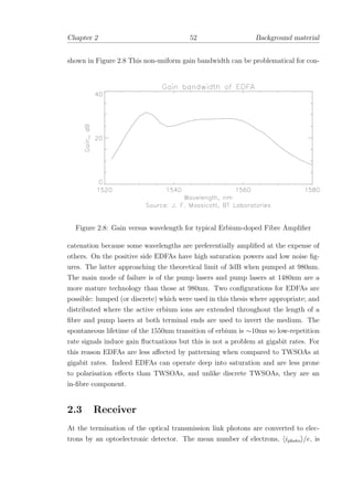

![Chapter 2 54 Background material
Because of the absense of photons for a logical ‘0’ no errors can result. Errors only
occur when a logical ‘1’ is transmitted but no photons are converted to photoelec-
trons. This is formally expressed as
p(0, N ) = N 0 e− N
0!
= 10−9
(2.87)
and so N ≈ 21 photons are required to ensure no more than one error for every
10−9
bits (a BER of 10−9
.) Therefore, for a quantum limited signal containing an
equal number of ‘1’s and ‘0’s the average optical power required is,
P = 21
hc
2ηλT
(2.88)
where, T, is the bit period. In practical systems the quantum limit is never reached
because electronic fluctuations akin to brownian motion within the detector gives rise
to current fluctuations or noise [53]. The photodetector has a finite dark current
which is independent of the noise from the low noise amplifier Figure 2.9. For
example the load bias contributes thermal noise. The low-noise amplifier circuit
contributes additional thermal noise and shot noise. The most significant noise
contribution in an amplified transmission system is due to optical amplifiers placed
between the source and the receiver to compensate for the fibre attenuation and to
improve the signal-to-noise ratio at the detector.
2.3.1.1 Thermal and shot noise
The two main electronic noise components are shot noise and thermal noise. The
total current generated by the receiver, I(t), then contains contributions from the
signal and noise components.
I(t) = iphoto + ishot + ith. (2.89)
The shot noise variance (or shot noise power), σs, is given by Equation 2.90
σ2
s = 2e( iphoto + Id)∆f (2.90)
and is due to statistical fluctuations arising from the discrete nature of electrons
within the receiver. With no optical power incident to the receiver ( iphoto = 0 )
only the dark current contribution, Id, remains. However by restricting the electrical
bandwidth, ∆f, its contribution can be reduced but care must be exercised to match
the electrical bandwidth to the data format (RZ or NRZ) and bit-rate of the incident
data. Because shot-noise masks quantum noise is dependent on the photocurrent](https://image.slidesharecdn.com/a1b5bb05-a929-4e33-93de-a2dfe5b88eed-160311214335/85/thesis-73-320.jpg)
![Chapter 2 55 Background material
it affects logical ‘1s’ more than logical ‘0s.’ (The finite dark current provides the
baseline.) The thermal noise variance, σth., is given by Equation 2.91,
σ2
th. =
4kT
R
∆f (2.91)
describes the thermally-induced fluctuations of electrons within the resistive ele-
ments of the receiver. It is independent of the photocurrent or dark current and so
affects both logical ’1s’ and ’0s.’ Once again it can be controlled by limiting the
electrical bandwidth of the device. Alternatively its effect could be reduced by low-
ering the temperature, but in lightwave systems this is not a practical proposition.
Thermal noise usually dominates shot noise in unamplified systems and is the main
noise mechanism. The signal-to-noise ratio (SNR) for an unamplified system can
then be represented by Equation 2.92
SNR =
R2
P2
in
2e( iphoto + Id)∆f + 4kTFn∆f
R
(2.92)
2.3.1.2 Optical amplifier noise
Many optical fibre transmission links employ in-line optical amplifiers to boost the
signal power and compensate for transmission loss, as outlined in the previous sec-
tion. Unfortunately optical amplifiers also add noise in the form of amplified spon-
taneous emission (ASE.) In the direct (or square-law) detection process described
in this thesis both the signal and ASE photons are indistinguishable after optoelec-
tronic conversion. Therefore it was necessary to minimise the proportion of ASE
contained in the optical signal by using optical filtering. So by combining Equa-
tion 2.79 with Equation 2.85 gives Equation 2.93 for the amplified photocurrent,
iphoto = RPinG (2.93)
The ASE spectral power density, S(ν), which is a useful measure of the ASE noise
energy is given by Equation 2.94
S(ν) = (G − 1)nsphν, (2.94)
It is possible to express the modified shot noise power and the additional ASE-related
noise powers in terms of the ASE spectral density as follows [54]
σ2
shot = 2eR (PinG + S(ν)∆ν) ∆f, (2.95)
σ2
sig−sp = 4 (RPinG) (RS(ν)∆f) , (2.96)](https://image.slidesharecdn.com/a1b5bb05-a929-4e33-93de-a2dfe5b88eed-160311214335/85/thesis-74-320.jpg)
![Chapter 2 56 Background material
σ2
sp−sp = R2
S2
(ν) (2∆ν − ∆f) ∆f. (2.97)
By restricting the optical bandwidth with a filter, the dominant noise component
is signal-spontaneous beat noise. Therefore the SNR at the output of the receiver
is [54] given by Equation 2.98,
SNR ≈
R2
P2
inG2
4 (RPinG) (R(G − 1)nsphν∆f)
≈
Pin
4nsphν∆f
(2.98)
This provides a practical prescription for maximising the SNR of a transmission link
that includes optical amplification. Firstly, the electrical bandwidth of the receiver,
∆f, should be sufficently small to accomodate the optical bit rate, B. For return
to-zero format used in the experiments described in this thesis this translates to
∆f = B. The presence of the spontaneous emission factor, nsp, highlights that it
is important that the amplifier be fully inverted or equivalently have the minimum
noise figure achievable.
Park and Granlund [55] have presented an appealing exposition of the beneficial
effects of using optical EDFA pre-amplification to improve the receiver sensitivity of
a transmission system. The BER of a lightwave system is derived from the Q factor
(Q = 6 for a 10−9
BER),
BER =
1
√
2π
exp(−Q2
2
)
Q
(2.99)
where,
Q =
Isig(1) − Isig(0)
σ(1) + σ(0)
(2.100)
here Isig(1) and Isig(0) are the signal current for a data ‘1’ and ‘0’ respectively; σ(1)
and σ(0) are the noise currents for data ‘1’ and ‘0’ respectively. The signal currents
are given by,
Isig(1) =
r
r + 1
· 2 P · ηinGηoutL · ηr
eη
hν
(2.101)
Isig(0) =
1
r + 1
· 2 P · ηinGηoutL · ηr
eη
hν
(2.102)
and include the effect of the finite extinction ratio, r, of the source. In addition,
P , is the average input power to the EDFA; ηin and ηout are, respectively, the
input and output loss of the amplifier; ηr is the loss between the receiver and the
photodetector; (L is any additional lumped loss;) G is the amplifier gain. The
final term represents the photocurrent conversion factor where e is the electronic
charge; h is Plancks constant; and ν is the signal frequency. The noise power, σ2
,
Equation 2.103 implicitly contains the noise contribution for a data ‘1’ and a data](https://image.slidesharecdn.com/a1b5bb05-a929-4e33-93de-a2dfe5b88eed-160311214335/85/thesis-75-320.jpg)
![Chapter 2 57 Background material
‘0’ through Equation 2.101 and Equation 2.102.
σ2
= σ2
shot + σ2
sig−spon + σ2
spon−spon + σ2
circ. (2.103)
The noise contributions that add to give the total noise power include the shot noise
power, σ2
shot,
σ2
shot = 2(Isig + Ispon · e∆f (2.104)
where, Ispon, represents the spontaneous noise photocurrent within the receiver and
is given by,
Ispon = 2 · S(ν)hν∆ν · ηoutLηr. (2.105)
The next term is the signal-spontaneous emission beat noise power, σ2
sig−spon,
σ2
sig−spon = 2 · IsigIspon ·
∆f
∆ν
(2.106)
and the spontaneous-spontaneous beat noise power, σ2
spon−spon,
σ2
spon−spon = I2
spon ·
∆f
∆ν
· 1 −
∆f
2∆ν
(2.107)
The equivalent receiver circuit noise, σ2
circ,
σ2
circ = ρ(ν) · ∆f ·
eη
hν
. (2.108)
where ρ(ν) is the noise current spectral density of the receiver circuit.
2.3.2 Power penalty
The power penalty represents the additional optical power that must be supplied to
the receiver to overcome noise. Other degradation mechanisms include timing jitter,
source chirp and fibre dispersion. These serve to transfer photons into adjacent time
slots which also lead to errors in system measurements. A baseline BER, commonly
called the “back-to-back,” corresponds to the bit-error rate at measured by the
receiver immediately after the modulated source i.e before fibre transmission an
amplification. Typically the penalty of the system is quoted for a BER at 10−9
. In
a badly degraded system additional power incident to the receiver does not improve
the BER measurement. In this case the signal is saturated with noise producing an
“error-floor” when BER values are plotted versus received optical power [56, 57].](https://image.slidesharecdn.com/a1b5bb05-a929-4e33-93de-a2dfe5b88eed-160311214335/85/thesis-76-320.jpg)
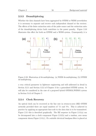

![Bibliography
[1] C. E. Shannon, “A mathematical theory of communication,” Bell Sys. Tech.
J., vol. 27 (XXVII), pp. 379–423, July 1948.
[2] Optoelectronic Industry and Technology Development Association (OITDA)
Newsletter no. 2, 1996. http://www.oitda.or.jp/news letter-2.html.
[3] N. Holonyak, “The semiconductor laser: A thirty-five year perspective,” Proc.
IEEE, vol. 85, pp. 1678–1693, November 1997.
[4] J. Von Neumann, “Notes on the photon-disequilibrium-amplification scheme
(JvN), september 16, 1953,” IEEE J. Quantum Electron., vol. 23, no. 6, pp. 659–
673, 1987.
[5] R. D. Dupuis, “An introduction to the development of the semiconductor laser,”
IEEE J. Quantum Electron., vol. 23, no. 6, pp. 651–657, 1987.
[6] R. N. Hall, G. E. Fenner, J. D. Kingsley, T. J. Soltys, and R. O. Carlson, “Coher-
ent light emission from GaAs junctions,” Phys. Rev. Lett., vol. 9, pp. 366–368,
Nov. 1 1962. (Received Sept. 24, 1962).
[7] M. I. Nathan, W. P. Dumke, G. Burns, F. H. Dill, and G. Lasher, “Stimu-
lated emission of radiation from GaAs p-n junctions,” Appl. Phys. Lett., vol. 1,
pp. 62–64, Nov. 1 1962. (Received Oct. 6, 1962).
[8] T. M. Quist, R. H. Rediker, R. J. Keyes, W. E. Krag, B. Lax, A. L. McWhorter,
and H. J. Zeiger, “Semiconductor maser of GaAs,” Appl. Phys. Lett., vol. 1,
pp. 91–92, Dec. 1 1962. (Received Oct. 23, 1962, in final form Nov. 5, 1962.).
[9] N. Holonyak and S. F. Bevacqua, “Coherent (visible) light emission from
Ga(As1−xPx junctions,” Appl. Phys. Lett., vol. 1, pp. 82–83, Dec. 15 1962.
(Received Oct. 17, 1962).
60](https://image.slidesharecdn.com/a1b5bb05-a929-4e33-93de-a2dfe5b88eed-160311214335/85/thesis-79-320.jpg)
![Chapter 2 61 BIBLIOGRAPHY
[10] F. Capasso, “Band-gap engineering: From physics and materials to new semi-
conductor devices,” Science, vol. 235, no. 2, pp. 172–176, January 1987.
[11] K. Y. Lau and A. Yariv, “Ultra-high speed semiconductor lasers,” IEEE J.
Quantum Electron., vol. QE-21, pp. 121—138, February 1985.
[12] K. Y. Lau, “Short-pulse and high-frequency signal generation in semiconductor
lasers,” IEEE J. Lightwave Technol., vol. LT-7, pp. 400–419, February 1989.
[13] I. H. White, “Picosecond optical pulse generation using semiconductor lasers,”
in Laser Sources and Applications: Proceedings of the 47th Scottish Universities
Summer School in Physics (A. Miller and D. M. Finlayson, eds.), NATO Ad-
vanced Study Institute, ch. 13, pp. 63–84, Bristol and Philadelphia: Institute
of Physics, 1996.
[14] P. V. Mamyshev, “Fibre nonlinearities,” in Laser Sources and Applica-
tions: Proceedings of the 47th Scottish Universities Summer School in Physics
(A. Miller and D. M. Finlayson, eds.), vol. 47 of NATO Advanced Study Insti-
tute, ch. 13, pp. 369–410, Bristol and Philadelphia: Institute of Physics, 1996.
[15] A. Hadjifotiou, “Optical modulators,” lecture notes, MSc in the physics of laser
communications, Physics Department, University of Essex, UK, 1994.
[16] J. S. Toll, “Causality and the dispersion relation: Logical foundations,” Phys.
Rev., vol. 104, pp. 1760–1770, December 1956.
[17] C. H. Henry, “Theory of the linewidth of semiconductor lasers,” IEEE J. Quan-
tum Electron., vol. QE-18, pp. 259–264, February 1982.
[18] T. H. Wood, “Multiple quantum well (MQW) waveguide modulators,” J. Light-
wave Technol., vol. LT-6, pp. 743–757, June 1988.
[19] R. C. Alferness, “Waveguide electrooptic modulators,” IEEE Trans. Microwave
Theory Tech., vol. MTT-30, no. 8, pp. 1121–1137, August 1982.
[20] P.-K. Lau, “Effects of laser diode parameters on power penalty in 10Gbit/s
optical fibre transmission systems,” IEEE J. Lightwave Technol., vol. LT-15,
pp. 1663–1668, February September 1997.](https://image.slidesharecdn.com/a1b5bb05-a929-4e33-93de-a2dfe5b88eed-160311214335/85/thesis-80-320.jpg)
![Chapter 2 62 BIBLIOGRAPHY
[21] W. Bogner, E. Gottwald, A. Scho¨pflin, and C. J. Weiske, “40Gbit/s unre-
peatered optical transmission over 148km by electrical time division multi-
plexing and demultiplexing,” Electron. Lett., vol. 33, no. 25, pp. 2136–2137,
December 1997.
[22] R. S. Tucker, G. Eisenstein, and S. K. Korotky, “Optical time-division mul-
tiplexing for very high bit-rate transmission,” IEEE J. Lightwave Technol.,
vol. LT-6, pp. 1737–1749, November 1988.
[23] W. Bogner, “40Gbit/s decision, demultiplexer and clock recovery circuit for ul-
trahigh speed optical transmission systems,” submitted to Electron. Lett., 1999.
[24] K. Takahata, Y. Miyamoto, Y. Muramoto, and Y. Matsuoka, “Ultrafast mono-
lithic receiver OEIC module operating at over 40Gbit/s,” Electron. Lett.,
vol. 35, no. 4, pp. 322–324, February 1999.
[25] K. Smith, J. K. Lucek, R. J. Manning, and K. J. Blow, “Advances in nonlinear
optics for information processing and all-optical networking,” Phil. Trans. R.
Soc. Lond. A, vol. 354, pp. 707–717, 1996.
[26] A. D. Ellis, K. Smith, and D. M. Patrick, “All optical clock recovery at bit rates
up to 40Gbit/s,” Electron. Lett., vol. 29, no. 15, pp. 1323–1324, July 1994.
[27] W. A. Pender, T. Widdowson, and A. D. Ellis, “Error free operation of a 40
Gbit/s all-optical regenerator,” Electron. Lett., vol. 32, no. 6, pp. 567–569,
March 1996.
[28] R. P. Feynman, QED: The strange theory of light and matter. New York:
Penguin, 1st ed., 1982.
[29] R. P. Feynman, R. B. Leighton, and M. Sands, “Quantum behavior,” in Quan-
tum Mechanics, vol. 3 of The Feynman lectures on Physics: Commemorative
issue, ch. 1, pp. 1–11, Reading, MA: Addison-Wesley, 1 ed., 1989.
[30] W. Van Etten and J. van der Platts, Fundamentals of Optical Fiber Communi-
cations. International Series in Optoelectronics, London: Prentice-Hall, 1 ed.,
1991.
[31] C. Kao and E. Hockham, “Dielectric-fibre surface waveguides for optical fre-
quencies,” Proc. IEEE, vol. 113, pp. 1151–1158, July 1966.](https://image.slidesharecdn.com/a1b5bb05-a929-4e33-93de-a2dfe5b88eed-160311214335/85/thesis-81-320.jpg)
![Chapter 2 63 BIBLIOGRAPHY
[32] J. E. Midwinter and Y. L. Guo, Optoelectronics and Lightwave Technology.
Chicester: Wiley, 1st ed., 1992.
[33] D. Marcuse, “Gaussian approximation of the fundamental modes of a graded-
index fibers,” J. Opt. Soc. Am., vol. 68, no. 1, pp. 103–109, January 1978.
[34] D. L. Williams. Private Communication, BT Laboratories, 9th June 1997.
[35] Unknown, “Corning SMF-28 CPC6 single-mode optical fiber,” October 1994.
Product information: PI1036, source http://www.corningfiber.com.
[36] G. P. Agrawal, “Optical fibers,” in Fiber-Optic Communication Systems
(K. Chang, ed.), Wiley series in microwave and optical engineering, ch. 2,
pp. 22–74, New York: Wiley, 1 ed., 1992.
[37] J. A. Armstrong, N. Bloembergen, J. Ducuing, and P. S. Pershan, “Interac-
tions between light waves in a nonlinear dielectic,” Phys. Rev., vol. 127, no. 6,
pp. 1918–1939, September 1962.
[38] P. V. Mamyshev, “Non-linearities in fibers and optical data transmission,” lec-
ture notes, 47th scottish universities summer school in physics, AT&T Bell
Laboratories, Holmdel New Jersey, July 1995. NATO Advanced Study Insti-
tute.
[39] M. Liu, “Optical fiber soliton transmission,” in Principles and applications of
optical communications, ch. 18, pp. 897–941, Chicago: Irwin, 1 ed., 1996.
[40] I. S. Gradshteyn and I. M. Ryzhik, “Definite integrals of elementary functions,”
in Tables of integrals, series, and products (A. Jeffrey, ed.), ch. 3 Exponential
functions, p. 307, London: Academic Press, corrected and enlarged uk edi-
tion ed., 1980. 2nd printing 1981.
[41] D. Wood, “Constraints on the bit rates in direct detection optical communica-
tion systems using linear or soliton pulses,” J. Lightwave Technol., vol. LT-8,
pp. 1097–1106, July 1990.
[42] Y. Sasaki, “Long-length low-loss polarization maintaining fibres,” IEEE J.
Lightwave Technol., vol. LT-5, no. 9, pp. 1139–1146, September 1987.
[43] P. N. Butcher and D. Cotter, The elements of nonlinear optics. Cambridge:
Cambridge, 1st ed., 1990.](https://image.slidesharecdn.com/a1b5bb05-a929-4e33-93de-a2dfe5b88eed-160311214335/85/thesis-82-320.jpg)
![Chapter 2 64 BIBLIOGRAPHY
[44] M. Nakazawa, “Soliton amplification in erbium-doped fiber amplifiers and its
application to soliton communication,” in Optical Solitons–Theory and experi-
ment (J. R. Taylor, ed.), Cambridge Studies in Modern Optics, ch. 6, pp. 152–
196, Cambridge: Cambridge, 1 ed., 1992.
[45] G. P. Agrawal, “Soliton communication systems,” in Fiber-Optic Communica-
tion Systems (K. Chang, ed.), Wiley series in microwave and optical engineering,
ch. 9, pp. 391–428, New York: Wiley, 1 ed., 1992.
[46] J. K. Lucek and K. J. Blow, “Soliton self-frequency shift in telecommunications
fibre,” Phys. Rev. A, vol. 45, no. 9, pp. 6666–6674, May 1992.
[47] L. F. Mollenauer, “Solitons in optical fibern: An experimental account,” in
Optical Solitons–Theory and experiment (J. R. Taylor, ed.), Cambridge Studies
in Modern Optics, ch. 2, pp. 30–60, Cambridge: Cambridge, 1 ed., 1992.
[48] A. D. Ellis, T. Widdowson, J. V. Wright, and E. Greer, “Nonlinear propagaton
effects,” in High capacity optical transmission explained (D. M. Spirit and M. J.
O’Mahoney, eds.), The Wiley-BT series, ch. 4, pp. 89–146, Chichester: Wiley,
1 ed., 1995.
[49] G. P. Agrawal, “Optical amplifiers,” in Fiber-Optic Communication Systems
(K. Chang, ed.), Wiley series in microwave and optical engineering, ch. 8,
pp. 329–390, New York: Wiley, 1 ed., 1992.
[50] M. Liu, “Optical amplification,” in Principles and applications of optical com-
munications, ch. 17, pp. 853–896, Chicago: Irwin, 1 ed., 1996.
[51] M. J. O’Mahoney, “Semiconductor laser optical amplifiers for use in future fibre
systems,” IEEE J. Lightwave Technol., no. 4, pp. 531–544, April 1988.
[52] J. L. Zyskind, C. R. Giles, J. R. Simpson, and D. J. DiGiovanni, “Erbium doped
fiber amplifiers and the next generation of lightwave systems,” AT&T Tech. J.,
pp. 53–62, January/February 1992.
[53] J. R. Pierce, “The origins of information theory,” in An Introduction to Infor-
mation Theory: Symbols, Signal and Noise, ch. 2, pp. 19–44, New York: Dover
Publications, Inc, 2 ed., 1980.
[54] M. Ming-Kang Liu, Principles and applications of optical communications.
Chicago: Irwin, 1st ed., 1996.](https://image.slidesharecdn.com/a1b5bb05-a929-4e33-93de-a2dfe5b88eed-160311214335/85/thesis-83-320.jpg)
![Chapter 2 65 BIBLIOGRAPHY
[55] Y. K. Park and S. W. Granlund, “Optical preamplifier receivers: Application
to long-haul digital transmission,” Opt. Fiber Technol., vol. 1, no. 1, pp. 59–71,
October 1994.
[56] K. Hinton and T. Stephens, “Modelling high-speed optical transmission sys-
tems,” IEEE J. Sel. Areas. Commun., vol. 11, no. 3, pp. 380–392, April 1993.
[57] G. P. Agrawal, “Optical detectors and receivers,” in Fiber-Optic Communica-
tion Systems (K. Chang, ed.), Wiley series in microwave and optical engineering,
ch. 4, pp. 174–176, New York: Wiley, 1 ed., 1992.](https://image.slidesharecdn.com/a1b5bb05-a929-4e33-93de-a2dfe5b88eed-160311214335/85/thesis-84-320.jpg)


![Chapter 3 68 OTDM Pulse Sources
tion ratio of the optical pulse source following time-interleaving at the transmitter.
There are two contributions: firstly, from its neighbours—lightly shaded regions ‘1’
and ‘2’ in Figure 3.1(a); and secondly arising from the neighbouring channels, in-
turn, interfering with one another—heavily shaded region ‘3’ in Figure 3.1(a). These
effects can be generalised for an N channel OTDM system via Equation 3.1 [1]
SNRi = Pi(t)dt/
n m=n
Pn(t)Pm(t)dt, (3.1)
where SNRi is the signal-to-noise ratio of the target channel and Pn(t) is the time
dependence of the power of channel n after demultiplexing at the receiver. Figure 3.2
illustrates the results when this model is applied to a 16 channel × 2.5 Gbit/s OTDM
Figure 3.2: SNR vs. pulsewidth dependence on extinction ratio. Variation of signal-
to-noise ratio as a function of RZ pulsewidth for several pulse extinction ratios from
40dB-54dB. (A 15ps FWHM gaussian demultiplexing window with an extinction
ratio of 100dB was used at the receiver.)
system that was representative of the SynchroLAN demonstrator. (A 15ps FWHM
gaussian demultiplexing window with an extinction ratio of 100dB was used at the
receiver.) These simulations suggested that to achieve a BER of 10−12
(⇒ Q = 7)
that corresponds to an SNR of 16.9dB (Q =
√
SNR,) an RZ pulse source with an
extinction ratio of ∼46dB and with a full-width half-maximum (FWHM) pulsewidth
in the range ∼5–6ps was required.](https://image.slidesharecdn.com/a1b5bb05-a929-4e33-93de-a2dfe5b88eed-160311214335/85/thesis-87-320.jpg)

![Chapter 3 70 OTDM Pulse Sources
varying, relative movement of the demultiplexing window with respect to the centre
of the target channel. It is worth mentioning that the effect of the finite rise- and fall-
time of the switching window is now important since it directly converts the timing
jitter into amplitide jitter and an intensity noise penalty in the received signal. This
is distinct from the capture of adjacent channels during the timing excursions of the
switching window.
3.2.2.1 Extinction ratio
The contribution of the finite demultiplexer extinction ratio is modelled with Equa-
tion 3.2 [1]
∆Pi = 10 log10
Pi(t)dt + k=i Pk(t)dt
Pi(t)dt − k=i Pk(t)dt
(3.2)
where, ∆Pi, is the power penalty of the target channel, i, arising from the finite
extinction ration of the demultiplexer. Pi(t) represents the time-dependence of the
signal power in the target channel. The time-dependence of the noise power in
the rejected channels (denoted by k, where k = i) is provided by the k=i Pk(t)dt
terms. The numerical procedure considered the 16 channel ×2.5 Gbit/s SynchroLAN
system. The RZ optical pulses were modelled as 4ps FWHM, sech2
pulses. The
demultiplexing window was gaussian and the simulation was repeated for a selection
of extinction ratio values, XR, ranging from 15dB–39dB. The results are presented
in Figure 3.4 which depict the power penalty incurred for several extinction ratios
Figure 3.4: BER penalty versus demultiplexing switching window of a 40Gbit/s RZ
system: (a) 19-27dB extinction ratio. (Note: XRs = “Extinction Ratios.”)](https://image.slidesharecdn.com/a1b5bb05-a929-4e33-93de-a2dfe5b88eed-160311214335/85/thesis-89-320.jpg)
![Chapter 3 71 OTDM Pulse Sources
ranging from 15–27dB. It is apparent that to achieve a power penalty of less than 1dB
then a demultiplexer extinction ratio in excess of 23dB is required when the width of
the demultiplexing window lies between 10–16ps. Figure 3.5 presents an additional
Figure 3.5: BER penalty versus demultiplexing switching window of a 40Gbit/s RZ
system: (a) 29-39dB extinction ratio. (Note: XRs = ”Extinction Ratios.”)
set of plots for extinction ratios in the range 29-39dB. As an example of the trade-
offs possible, a demultiplexing extinction ratio of 27dB is very tolerant to switching
window widths from 3–18 ps. Conversely, the extinction ratio requirement can be
relaxed but at the expense of narrower switching window widths. Section 3.2.2.2
will illustrate how this tolerance of the switching window width can be exploited to
accomodate timing jitter.
3.2.2.2 Timing jitter
Consider the three successive OTDM pulses illustrated in Figure 3.6(a) which depicts
the target channel, i, precededed by channel, i − 1, and succeeded by channel, i + 1.
The pulse period is represented by, T, and the square switching window (indicated
by the dashed line) has width, W. The model used to estimate the effect of the RMS
timing jitter and the width of the switching window on the system penalty follows
that presented by Jinno [2] and makes three assumptions: 1) the optical pulsewidth
is much shorter than, W, the switching window width; 2) the jitter is approximated
by a gaussian probability distribution function (PDF); and 3) the optical pulses have
identical RMS timing jitter, σ. Figure 3.6(b) represents the gaussian PDF of timing
jitter. The area denoted by the dashed region in the tails represents the probaility](https://image.slidesharecdn.com/a1b5bb05-a929-4e33-93de-a2dfe5b88eed-160311214335/85/thesis-90-320.jpg)


![Chapter 3 74 OTDM Pulse Sources
switching window and hence no account is taken in the model of the appreciable rise-
and fall- times likely to be present in a practical demultiplexing device. Nevertheless
based on these constraints some suitable guiding principles for the system are: 1)
the demultiplexing window should be less than 15ps; 2) the RMS jitter of the optical
pulse source should be less than 1ps; 3) the demultiplexer extinction ratio should be
in excess of 27dB; and finally, 4) from Figure 3.2 the source extinction ratio should
be at least 46dB.
3.3 Gain-Switched DFB (GS-DFB) pulse sources
3.3.1 Introduction
It is well-known that a train of frequency-chirped return-to-zero optical pulses can
be created if an external electrical generator is used to impress a periodic modulation
upon a DC-biased semiconductor laser diode (SLD) [3]. The electrical modulation
injects charge carriers into the active region of the laser building up a sizable gain
inversion before the onset of lasing. It is helpful to consider a modulated SLD
as a capacitor with a finite rise time where the stored charge within the active
region is optically discharged—triggered by a spontaneous photon when the photon
density exceeds the stimulated emission threshold. The result—a pulse of coherent
radiation—discharges the capacitor to deplete the gain inversion. If the steady state
photon density does not fully recover to its equilibrium value before the application
of a subsequent electrical pulse or if the amount of charge deposited is too great
or is deposited in too long a period of time, then relaxation oscillations can occur.
These result from the dynamic coupling between the photon and electron densities
within the active layer.
Studies into the optical characteristics of injection lasers subject to electrical
modulation started in 1966 when Kurnosov et al [4] applied isolated, 600ns dura-
tion, electrical pulses of amplitude between 1–5A to a GaAs semiconductor laser
cooled to 77K. They observed self-modulation (or spiking1
) of the emitted light.
They also noted that the interval between spikes decreased as the electrical pulse
amplitude was increased above the threshold current of 1.85A. The following year,
Roldan [5] performed similar experiments at room temperature. He applied 50 ns
electrical pulses to a GaAs SLD at a repetition rate of 100Hz. Again as the ampli-
tude of the current pulse was increased above threshold, the number of relaxation
1
What are now more commonly termed relaxation oscillations.](https://image.slidesharecdn.com/a1b5bb05-a929-4e33-93de-a2dfe5b88eed-160311214335/85/thesis-93-320.jpg)
![Chapter 3 75 OTDM Pulse Sources
oscillations increased. But in addition, the turn-on delay between the application of
the current pulse and the production of the first optical spike decreased. The turn-
on delay was maximised and a single optical spike was observed (corresponding to
the first relaxation oscillation) when the laser was biased slightly above threshold
(1.006Ith). In particular the isolated light spike or pulse appeared at the very end
of the electronic current pulse.
Tarucha and Otsuka [6] studied the optical response of a DC-biased multimode
AlGaAs SLD subjected to a deep sinusoidal RF injection current. They began by
solving the coupled photon and carrier density equations numerically and then com-
pared the results with experimental measurements. Multiple peaks characteristic
of relaxation oscillations were observed at low electrical drive frequencies. As the
modulating frequency was increased the number of peaks was reduced until only
the first peak of the relaxation oscillation was excited. This resulted in a train of
optical pulses with FWHM of between 40–70ps. At higher modulating frequencies
patterning was observed which eventually gave way to period doubling whereby two
modulating cycles of the RF signal were required to produce a single optical pulse.
The onset of this behaviour was gradual and could be delayed by increasing the
DC bias current. Single optical pulse generation occurred within a specific modu-
lating frequency interval or band. Below this frequency band relaxation oscillations
dominated. Above this frequency band a regime leading to period doubling was
recorded where successive pulses retained a memory of their predecessors. From
this study it was possible to appreciate that gain switching, as this method came
to be called, occupied a frequency interval bounded between relaxation oscillations
at low frequencies and pattern dependency and eventually period doubling at high
frequencies.
Au Yeung [7] was the first to demonstrate gain-switching at rates above 1GHz.
Here an electrical sinusoid was rectified so that only the positive-going amplitude
cycle was applied to the laser chip. In this way 28ps gaussian optical pulses were
produced at 2.5GHz at near-zero DC bias. Van der Ziel et al. [8] applied both a
sinusoidal modulation and an impulse modulation—the latter from a 940MHz step-
recovery diode (SRD) which is also denoted as an impulse generator (IG.) They
suggested that impulse modulation was required to produce temporally short optical
pulses. They further considered the effect of device length on the optical pulses
produced, in particular noting that the optical pulsewidth decreased for the shorter
devices due to the reduction in the parasitic capacitance of the shorter packages.
However the shorter devices produced less optical power. Consequently there was](https://image.slidesharecdn.com/a1b5bb05-a929-4e33-93de-a2dfe5b88eed-160311214335/85/thesis-94-320.jpg)
![Chapter 3 76 OTDM Pulse Sources
a compromise to be found between pulsewidth and optical power since the shorter
devices (125µm) produced 19ps FWHM pulses, the longer versions (380µm) 24ps
FWHM pulses. Higher levels of current injection tended to produce multiple pulses
or relaxation oscillations. In addition ‘narrow spikes’ were observed superimposed
upon the autocorrelation profile that arose from the coherent interference of the
several longitudinal cavity modes within the gain switched optical pulses. They
further observed that the pulse width decreased with increasing DC-bias and RF
current. In 1985 Downey et al. [9] presented a comprehensive study of gain-switching
where they used short, 17ps FWHM, electrical pulses derived from a 300fs optical
pulse that were applied to a picosecond photoconductive switch based on an ion-
bombarded InP photoconductor at 120MHz. The gain switched optical pulses that
resulted were asymmetric with the 90-10 falltime typically twice the 10/90 risetime.
Both the rising and falling edges of the optical pulse were well approximated by
exponential functions which were consistent with an asymmetric sech2
-type pulse
profile.
All of the studies described used multimode Fabry-Perot lasers, this is unsuit-
able in practical high speed transmission systems because the competition between
the individual longitudinal modes causes an unstable spectral profile which is trans-
formed into timing jitter when the pulses are transmitted through a dispersive op-
tical fibre. The ideal, therefore, is to excite a single longitudinal mode. Onodera et
al. [10] were the first to demonstrate gain-switching of such a single-moded laser. In
their case a 1.294µm InGaAsP DFB (Ith = 44mA) produced pulses of 34ps FWHM
and spectral FWHM of (11.2GHz.) The resulting time-bandwidth product was 0.38.
However they assumed a lorentzian pulse, so their claim that the pulses were ‘Fourier
transform-limited’ must be discounted because a transform-limited lorentzian pulse
has a time-bandwidth product of 0.11. Interestingly they observed that changing
the DC-bias in the range (−2.5Ith < I < 0.8Ith) increased the measured pulse width,
∆t, over the range (25ps < ∆t < 40ps.)
So to summarise in gain-switching the first peak of the optical relaxation oscil-
lations is induced by appropriately terminating the electrical driving signal. The
idea is that a single electrical “spike” containing a just-sufficient quantity of charge
carriers produces a single optical pulse. Moreover since the relaxation frequency
is proportional to the DC-bias current, when the diode is biased below threshold
the relaxation oscillation frequency is reduced and one optical pulse is generated.
Above threshold the relaxation oscillation frequency is increased and multiple optical
pulses result. It is possible to prescribe that when the interval between the electrical](https://image.slidesharecdn.com/a1b5bb05-a929-4e33-93de-a2dfe5b88eed-160311214335/85/thesis-95-320.jpg)
![Chapter 3 77 OTDM Pulse Sources
pulses is sufficient to allow the photon density to return to its steady state, then
each optical pulse is generated independently of its predecessors. As this temporal
interval is decreased (repetition rate increased) a situation arises where the photon
density has not recovered to its equilibrium value before the application of another
electrical pulse which leads to patterning. There are several methods for generat-
ing electrical impulses suitable for gain-switching including Auston Switches [11];
Downey et al. [9] (as mentioned above) used a photoconductor but more typical
(and convenient) is the use of commercial step-recovery diodes/impulse generators
(SRDs/IGs) [12, 13]. Gain switching by use of a SRD/IG was first reported, almost
simultaneously, in 1980 [14, 15] with pulsewidths of 100ps and 42ps respectively.
SRDs/IGs are assigned a nominal frequency for operation, however as Figure 3.8
shows, an SRD rated for 500MHz that also operates effectively at other discrete sub-
harmonic frequencies, in this particular case 400MHz. Finally it is also desirable to
Figure 3.8: 400MHz electrical impulses from ‘500MHz’ Step-recovery diode/Impulse
generator.
use single-longitudinal mode DFB lasers for gain-switching to prevent the adverse
effects of mode-partition noise.
3.3.2 Theory
The rate equations: Equation 3.7
dn
dt
=
J(t)
ed
− g (n − nt) S −
n
τs
, (3.7)](https://image.slidesharecdn.com/a1b5bb05-a929-4e33-93de-a2dfe5b88eed-160311214335/85/thesis-96-320.jpg)
![Chapter 3 78 OTDM Pulse Sources
and Equation 3.8,
dS
dt
= Γg (n − nt) S −
S
τph
+ βΓ
n
τs
, (3.8)
for a single-mode semiconductor laser govern the temporal evolution of the carrier
density, n = n(t), to the photon density, S = S(t). The parameters are defined as
follows: J(t) is the current density; e is the electronic charge; d is the thickness of
the active layer; g is the differential gain coefficient; nt is the transparent carrier
density; τs is the carrier lifetime; β is the spontaneous coupling factor, that is, the
fraction of spontaneous emission that is coupled into the stimulated emission output;
Γ is the optical confinement factor [16]; τph is the photon lifetime given by,
τph =
1
vg(αm + αi)
(3.9)
with, vg, the group velocity of light within the active region; αm, the mirror loss;
αi, the internal loss (or the effective end loss due to distributed feedback.) If gain
compression, is neglected ( = 0) then the differential gain coefficient is given by go,
its small signal value, Equation 3.10,
g =
go
1 + S
≈ g0. (3.10)
Of note is that the stimulated emission term, g (n − nt)S, acts antagonistically
between Equation 3.7 and Equation 3.8 so that as the number of stimulated photons
increases, so the number of carriers decreases and vice-versa. The carrier density,
n(t), affects the optical pathlength within the cavity so that the emission frequency,
ν(t), varies or chirps according to, Equation 3.11,
ν(t) =
nt
nt − Γαg0
k
n(t)
ν0, (3.11)
where α, the linewidth enhancement factor [17]; k, the free space propagation con-
stant and ν0, the centre frequency at transparency [18]. The analysis presented by
White [19] provides a useful, intuitive, insight into the gain-switching process. The
main assumption is that a short electrical impulse is used to provide ∆n carriers in
excess of the transparent carrier density before photonic discharge i.e. S = 0 for
n = nt + ∆n. The carrier depletion during the emission of the gain switched pulse
is then modelled by a ‘tanh’ function such that,
n(t) = nt − ∆n tanh
t
τ
. (3.12)
Solving for the photon density, S(t), gives,
S(t) = So sech2 t
τ
. (3.13)](https://image.slidesharecdn.com/a1b5bb05-a929-4e33-93de-a2dfe5b88eed-160311214335/85/thesis-97-320.jpg)
![Chapter 3 79 OTDM Pulse Sources
It follows from Equation 3.13 that the pulsewidth, τ, is approximated by
|τ| ∼
1
g0∆n
. (3.14)
This indicates that to obtain short optical pulses the gain of the laser medium
and the number of excess carriers must be maximised. As an aside, it is worth
recalling the experimental observations of Downey et al. [9] that were discussed in
Section 3.3.1 on Page 76 which are consistent with a solution of the form,
Sasech(t) =
So
e−t/τr + e−t/τf
. (3.15)
This accounts for the rising, τr; and falling, τf, time constants of the gain-switched
optical pulse [20]. Section 3.3.3, will describe how the wavelength chirp can be
compensated by a suitable dispersive element typically a suitable length of optical
fibre or optical fibre grating to provide temporal pulse compression. In practice,
however, the chirp is non-monotonic which also necessitates spectral filtering.
3.3.3 Optical pulse generation: Linear pulse compression
DFB laser diodes share a parabolic material gain dependence as a function of wave-
length in common with Fabry-Perot lasers and semiconductor optical amplifiers.
However in a DFB laser the grating period defines the lasing wavelength [21]. It
is possible to engineer the chirp parameter of a DFB laser diode by virtue of the
spectral position of the lasing wavelength with respect to the wavelength of the maxi-
mum of the material gain. Historically when single longitudinal mode DFB-LDs were
used in coherent system experiments the main requirement was for minimum spec-
tral linewidth or low-chirp. Westbrook [22] amongst others [23, 24] prescribed that
for a low-chirp DFB laser, α—the linewidth enhancement factor, should approach
zero. For this the lasing wavelength should be located on the short-wavelength side
of the material gain maxima. In addition, Green [24] advocated the use of multi-
quantum well (MQW) DFB lasers over Heterostructure DFB lasers to further reduce
the chirp. But for optical pulse compression enhanced chirp is desirable and it is
better, therefore, that the lasing wavelength is located on the long-wavelength side
of the material gain maximum and that a heterostructure DFB laser diode is used.
It is possible to define the time-bandwidth product for a pulse with a gaussian in-
tensity, I(t), profile and with a linear chirp by equating the linewidth enhancement
factor, α, with the chirp parameter, C. In the case of a gain-switched DFB which
has a red-shifting (α = −C [25]) wavelength chirp, the time-bandwidth product [26]](https://image.slidesharecdn.com/a1b5bb05-a929-4e33-93de-a2dfe5b88eed-160311214335/85/thesis-98-320.jpg)
![Chapter 3 81 OTDM Pulse Sources
and directed to a background-free autocorrelator. The autocorrelation and spec-
tral profile of the output pulses are shown in Figure 3.10(a), and Figure 3.10(b)
Figure 3.10: (a) Autocorrelation of direct output from gain-switched DFB. (b) Spec-
tral plot of direct output from gain-switched DFB.
respectively. The FWHM temporal width of 19.3 ps and FWHM spectral width
of 1.56nm resulted in a time-bandwidth product ∆ν∆t of 3.83 which is indicative
of a highly chirped pulse. The spectral profile, Figure 3.10(b), is typical of a gain
switched pulse [27] being asymmetric and with a characteristic ‘shoulder-like’ short
wavelength spectral enhancement.
3.3.3.1 Dispersion compensating fibre
It was shown in Figure 3.2 that a 40Gbit/s OTDM system dictates a pulsewidth of
between 5–6ps. Clearly the 19.3ps pulses described in the last section are too broad
temporally. To remedy this a non-soliton supporting, dispersion compensating fibre
(DCF) was attached to port 2 of the 50/50 fused fibre coupler shown in Figure 3.9.
The DCF had a group velocity dispersion parameter, D, of +45 ps/nm/km and the
fibre length was cut-back to Lf = 300m where the minimum temporal pulsewidth
of 4.7ps was obtained, Figure 3.11(a). This is well within the pulsewidth require-
ment of 5–6ps. The absense of non-linear, “soliton-like,” compression effects is con-
firmed from the corresponding spectral profile and spectral width which remained
unchanged with ∆λ = 1.58nm, Figure 3.11(b). This gave a time-bandwidth prod-
uct, ∆ν∆t, of 0.95. For a transform-limited gaussian pulse ∆ν∆t ≈ 0.44 so the
pulses were not transform limited which is indicative of residual wavelength chirp.](https://image.slidesharecdn.com/a1b5bb05-a929-4e33-93de-a2dfe5b88eed-160311214335/85/thesis-100-320.jpg)
![Chapter 3 82 OTDM Pulse Sources
Figure 3.11: (a) Autocorrelation after 300m Dispersion Compensating Fibre (DCF.)
(b) Spectral plot after 300m DCF.
Despite this impairment and given the short distances envisaged for SynchroLAN
dispersive effects arising from transmission are unlikely to be a problem so this par-
ticular pulse source satisfies the pulsewidth requirements. However, as will be shown
in Section 3.3.5, timing jitter must still be addressed.
3.3.3.2 Step-chirped fibre grating
In the past spatial diffraction grating pairs have been been used successfully to
obtain temporal compression of the optical pulses generated from a gain-switched
SLD [28]. However the method is now less common because it requires both fine
adjustment and careful alignment of the external spatial diffraction grating pair
which are susceptible to mechanical perturbations and thermal instabilities. The
most common method used now is based on optical fibre bragg gratings that were
first demonstrated by Hill and co-workers in 1978 when they demonstrated how Ge-
doped optical fibres could form reflection filters (or gratings) in response to UV light-
induced changes to the refractive index [29]. Fibre gratings have many applications
as wavelength-demultiplexers, EDFA gain equalisers etc. [30]. Of particular note to
the present application is the work of Ouellette [31] who was the first to substitute
a chirped fibre grating for a DCF. The common attraction of DCFs and chirped
fibre gratings is that they are in-fibre devices and so are readily spliced to existing
fibre with low insertion loss. However, the chirped fibre grating is a more compact
device with the additional benefit that its finite stopband can provide useful spectral](https://image.slidesharecdn.com/a1b5bb05-a929-4e33-93de-a2dfe5b88eed-160311214335/85/thesis-101-320.jpg)
![Chapter 3 83 OTDM Pulse Sources
filtering.
To understand how a fibre grating works consider an optical fibre with a lon-
gitudinal (z-axis) modulation imposed onto its core refractive index, n(z), to form
a distributed grating structure with period ∼ Λ. A proportion of the light energy
at resonant, half-wavelength, multiples of the Bragg wavelength, Λ is scattered for-
wards, and a proportion is scattered backwards (or reflected.) This is represented
by Equation 3.17,
nΛ = m
λ
2
, (3.17)
which is Braggs law. The cumulative, coherent addition of the backward- and
forward-travelling electric fields forms a wavelength stop-band which is in effect
a region of reflection. The serial concatenation of several adjacent gratings along an
optical fibre, where the centre wavelength of the stop-band for each succesive grating
is monotonically incremented (or decremented,) forms a step-chirped fibre grating
(SCFG [32].) A SCFG therefore comprises, N grating sections of fixed length, δl,
with a different grating period, Λn, for each section. A schematic of a SCFG of
length, L, is shown in Figure 3.12 where Λn is the period of the nth
of N sections.
lδ lδ lδ lδ
Λ Λ Λ Λ1 2 3
L
N
Figure 3.12: Step Chirped Fibre Grating (SCFG) of length L schematic. Comprised
of N sections of equal length, δl, with periods ranging from Λ1 to ΛN .
The length of each section, δl, is simply,
δl =
L
N
, (3.18)
where the difference in period between successive sections, ∆Λ, is given by
δΛ =
δλ
N
. (3.19)](https://image.slidesharecdn.com/a1b5bb05-a929-4e33-93de-a2dfe5b88eed-160311214335/85/thesis-102-320.jpg)
![Chapter 3 84 OTDM Pulse Sources
The spatial position of each stop-band along the fibre length determines the point
of reflection of a particular wavelength interval. In operation the wavelength com-
ponents of an optical pulse incident to a SCFG are reflected from different positions
within the grating. This forms, in effect, several spatially-distributed, wavelength-
dependent mirrors. The total ‘time-of-flight’, Ttof
3
, between the first and last sec-
tions of the SCFG—a distance of Lg—is given by Equation 3.20,
Ttof =
2Lg
vg
. (3.20)
The net effect is a dispersion, D, over the wavelength interval, ∆λ.
It is possible to experimentally determine the parameters required of a SCFG
for temporal compensation by using a length of dispersion compensating optical
fibre that is cut-back to the optimum compression length, Lf. For a given group
delay dispersion parameter, D, the time-of-flight Equation 3.20 can be expressed as
Equation 3.21
DLf =
Ttof
∆λ
(3.21)
which, in turn, can be rewritten as, Equation 3.22,
DLf =
2n
c
1
λ2
∆ν
Lg
−1
(3.22)
where ∆ν is the grating bandwidth; n is the refractive index; and c is the velocity
of light in vacuum [33, 34]. In particular the term (∆ν/Lg)−1
can be considered
as the grating chirp parameter [35]. Now the leading (short wavelength) ‘blue’
components of the pulses emitted from a gain-switched DFB-LD precede the trailing
(longer wavelength) ‘red’ components. So by reflecting the ‘blue’ components from
the back of the grating and the red components from the front of the grating, pulse
compression is achieved. It is important to note that the DCF works in transmission
and is a non-resonant structure. On the other-hand the SCFG works in reflection
and is a resonant structure. This latter property has important implications for the
‘quality’ of the compressed pulses that are produced since it can be responsible for
additional temporal and spectral structure and the enhancement the pulse pedestal.
Eggleton et al. [36] used a quadratically chirped fibre grating to compress gain-
switched pulses to 14ps, which represented a temporal compression factor of 1.6. In
addition, ×5 compression was demonstrated from a gain-switched Fabry-Perot laser
diode with a 40mm long, strain-chirped, fibre grating that produced 12ps pulses [37].
3
Another useful rule of thumb is that light travels at 2 × 10⁸
m/s in an optical fibre or 1mm
= 5ps.](https://image.slidesharecdn.com/a1b5bb05-a929-4e33-93de-a2dfe5b88eed-160311214335/85/thesis-103-320.jpg)
![Chapter 3 85 OTDM Pulse Sources
In the present measurements that are described in Figure 3.9 the fibre length (300m)
and dispersion parameter (+45ps/nm/km) of the DCF were used to calculate an op-
timum dispersion for a SCFG of ∼ +13.5ps/nm. It was then possible to estimate the
requirements for a grating by assuming a linear chirp. This translated into a ∼27ps
delay for ∆λ ∼ 2nm corresponding to a grating length of ∼ 2.7mm (= 5.4/2mm).
A 6mm long SCFG with a spectral width of ∼ 3nm was then fabricated and spliced
to port 1. (The fabrication method is detailed elsewhere [38].) The transmission
band of the grating is shown in Figure 3.13. During the measurements the SCFG
Figure 3.13: Transmission spectrum of Step Chirped Fibre Grating (SCFG)
was suspended and clamped between two mechanical jaws which formed part of a
mechanically adjustable cradle that enabled tension-induced tuning of the grating
pass-band and by implication, chirp. After suitable adjustment via fibre tensioning,
temporally compressed pulses exited from port 3 (refer to Figure 3.9.) The autocor-
related pulses reflected from the SCFG shown in Figure 3.14(a) were slightly shorter
than those obtained from the DCF, with a temporal pulsewidth of 4.4ps. The spec-
tral filtering effect of the SCFG reduced the spectral width to 1.25nm, Figure 3.14(b),
which gave ∆ν∆t = 0.71. In an effort to further isolate the pulse from the pedestal
component a tunable filter with a FWHM spectral width of 1.16nm was inserted
between port 3 and the EDFA, (refer to Figure 3.9.) The temporal FWHM of the
autocorrelation increased to 5.1ps, Figure 3.15(a), and the corresponding spectral
width was reduced slightly to 1.05nm, Figure 3.15(b), giving ∆ν∆t = 0.47 which
was close to the transform-limited value of 0.44 expected for a pulse with a gaussian
temporal profile. Nevertheless the pedestal component persisted and could not be](https://image.slidesharecdn.com/a1b5bb05-a929-4e33-93de-a2dfe5b88eed-160311214335/85/thesis-104-320.jpg)
![Chapter 3 86 OTDM Pulse Sources
Figure 3.14: (a) Autocorrelation after Step Chirped Fibre Grating (SCFG) com-
pression; (b) corresponding spectral plot.
removed. The origin of the pedestal structure results from the interaction of the
non-linearly chirped spectral components with the discrete, discontinuous step-like
dispersion approximation of the resonant SCFG. It is these resonances that cause the
additional pedestal structure evident in the autocorrelation plot of Figures 3.14(a)
& 3.15(a). Ennser et al. [39] have described how this is due to the rapidly oscillating
modulation of the group delay with wavelength across the reflection band of fibre
grating stuctures. This same phenomena—time delay ripple—has been described
in the context of a 10Gbit/s optical transmission system [40]. For example apodi-
sation [41] together with the number of sections [32] have been shown to markedly
improve the delay characteristics of SCFG. On the positive side pulses of less than
5ps FWHM, were reported using this 6mm long fibre grating—a compression factor
of 4.3 which was probably the shortest pulses generated by this technique at the
time, and indicates how a properly tailored SCFG may be employed effectively for
pulse compression [42]. On the negative side, the persistent pedestal component
means that pulses compressed by the SCFG would give rise to a significant power
penalty after interleaving and are therefore unsuitable for the SynchroLAN appli-
cation. For this reason it is necessary to suffer the inconvenience of the physical
dimensions of the optical fibre spool because of the relative absence of pedestal
structure. Nevertheless it is interesting to speculate how a specially tailored fibre
grating with a non-linear chirp would allow the generation of even shorter optical
pulses by compensating for non-linear chirp components in the gain-switched DFB](https://image.slidesharecdn.com/a1b5bb05-a929-4e33-93de-a2dfe5b88eed-160311214335/85/thesis-105-320.jpg)
![Chapter 3 87 OTDM Pulse Sources
Figure 3.15: (a) Autocorrelation after SCFG compression and spectral filtering; (b)
corresponding spectral plot (dashed curve corresponds to Figure 3.14(b).)
output—this is something that is not currently possible with conventional optical
fibre compensation.
3.3.4 Optical pulse generation: Non-linear pulse compres-
sion
The last section demonstrated how a gain-switched DFB-SLD can be used with lin-
ear compression from either a DCF or step-chirped fibre grating to produce short
optical pulses of ∼5ps duration. This pulsewidth is sufficient for a 40Gbit/s OTDM
system yet it is useful to anticipate future upgrades of such an OTDM system to lin-
erates of 100Gbit/s and beyond. When the amount of pulse compression extracted
from a dispersion compensating fibre or a step-chirped optical fibre grating is ex-
hausted it is necessary to turn to compression techniques based on power-dependent
optical non-linearities within the optical fibre to provide additional temporal com-
presion. These techniques rely on self-phase modulation within an anomalously dis-
persive optical fibre to generate additional frequency components that broaden the
spectral width to provide additonal wavelength chirp. It is important to emphasise
that the self-phase modulation of the downchirped pulses, typical of gain-switched
DFBs, can actually serve to narrow the spectral profile which translates into pulse
broadening [43]. Two methods were investigated. The first used anomalously dis-
persive optical fibre of constant dispersion, the second employed an anomalously](https://image.slidesharecdn.com/a1b5bb05-a929-4e33-93de-a2dfe5b88eed-160311214335/85/thesis-106-320.jpg)


![Chapter 3 90 OTDM Pulse Sources
tween a soliton component and an undesirable dispersive wave component [44]. It is
the latter that forms the pedestal that would negatively impact the system penalty
and make these pulses unsuitable for time-interleaving. Because the autocorrelator
is a polarisation dependent element the rotation of a half-wave plate at its entrance
made it possible to discriminate between the solitonic component and the linear
dispersive wave component of the pulse pulse. The soliton component is revealed
in Figure 3.19(a). Further rotation of the half-wave plate by 70◦
revealed a broad
Figure 3.19: (a) Solitonic component (half-wave plate 0 degrees); (b) dispersive wave
component (half-wave plate 70 degrees). Rep. rate 400MHz
structure which is the dispersive wave component (more accurately an autocorre-
lation between both the solitonic and dispersive wave components.) The solitonic
component is subjext to non-linear polarisation rotation (NPR) within the fibre.
It is possible to make the non-linear solitonic component orthogonal (90◦
) to the
dispersive-wave component by adjusting the power launched into the NLF. This is
then amenable to removal by an in-fibre polariser at the output of the NLF [45].
Unfortunately the slow evolution of the polarisation state of pulses within the sys-
tem would require active tracking in addition to careful monitoring of the launched
power into the NLF to maintain orthogonality between the two components. This
is an involved control problem that would require a complex implemention in a
practical system.](https://image.slidesharecdn.com/a1b5bb05-a929-4e33-93de-a2dfe5b88eed-160311214335/85/thesis-109-320.jpg)
![Chapter 3 91 OTDM Pulse Sources
3.3.4.2 Dispersion decreasing fibre
Soliton propagation in an optical fibre is described by the non-linear Schr¨odinger
(NLS) equation Equation 2.74. In the case of a fundamental, N = 1, soliton the
effect of optical fibre attenuation with propagation distance serves to reduce the
soliton pulse energy which causes a monotonic broadening of the pulsewidth. Con-
versely, if suitable amplification were provided to exactly compensate for the optical
fibre attenuation then a fundamental soliton would propagate unchanged. Interest-
ingly amplification slightly in excess of that required for compensation of the fibre
attenuation results in pulse compression as a fundamental soliton adapts to the per-
turbation by increasing its peak power and decreasing its pulsewidth. An effective
amplification can also be induced by a gradual, tapered reduction of the dispersion
parameter along the fibre axis in the direction of propagation [46]. To understand
why this is so recall that, < P >, the average power of a fundamental soliton, is
given by Equation 3.23 and if the various constants are neglected it is proportional
to the terms on the RHS of Equation 3.24,
<P > ∼
1
T
×
λ3
n2
|D|
τ
Aeff . (3.24)
Energy conservation dictates that the average power of a fundamental soliton at
the input and the output of an optical fibre remains unchanged. In addition, the
repetition rate, 1/T, the refractive index, n2 and the wavelength, λ, will also be
unchanged. The equality, Equation 3.25,
|D|in
τin
Ain =
|D|out
τout
Aout, (3.25)
then follows and it can be rearranged as Equation 3.26
τout =
|D|outAout
|D|inAin
τin. (3.26)
Hence if |D|outAout < |D|inAin then provided the transition is adiabatic a funda-
mental soliton will undergo temporal compression, τout < τin. Bogatyrev et al. [47]
determined that the adiabatic transtion required a hyperbolic dispersion profile with
the form of Equation 3.27,
D(z) =
Din
1 + 2Γz
, (3.27)
where use was made of Equation ??, and where Γ is the effective gain; z is the
propagation distance; and D(z) is the dispersion. One possible approach is to alter
the waveguide dispersion of the fibre which is directly related to the dispersion](https://image.slidesharecdn.com/a1b5bb05-a929-4e33-93de-a2dfe5b88eed-160311214335/85/thesis-110-320.jpg)
![Chapter 3 92 OTDM Pulse Sources
parameter, D. Such a dispersion decreasing fibre (DDF) was used successfully to
effect adiabatic soliton pulse compression using the hyperbolic dispersion profile
described by Equation 3.28 [48] below,
D(z) =
10
1 + 12z
. (3.28)
In that case the optical fibre fabrication was greatly aided by the use of a digital
computer-controlled, closed-loop feedback apparatus that allowed the pull-rate and
hence the dispersion profile of the fibre to be accurately controlled. The beat-
frequency pulse source generated pristine, transform-limited pulses, with FWHM
pulsewidths of 1.3ps at a repetition rate of 70 GHz. The drawback is that it would
prove difficult to modulate the optical pulses at such a high repetition rate.
To further investigate this approach a DDF was fabricated. Unfortunately the
optical fibre drawing facility that was available at BT Laboratories used a manually-
operated analog controller to vary the draw-rate and by implication the diameter of
the optical fibre pulled from the preform. It was difficult, therefore, to accurately
transfer the required hyperbolic profile onto the optical fibre. Nevertheless as an
approximation, a fibre was pulled such that the fibre drawrate was increased as a
function of drawn-length. The values used were determined using a fibre simulation
program that was developed at BT Laboratories. and are given in Table 3.1 The core
Distance Core Core Material Waveguide Total
(m) radius index dispersion dispersion dispersion
(nm) (ps/nm/km) (ps/nm/km) (ps/nm/km)
-400 2900 1.44 22.16 -10.21 11.95
0 2800 1.44 22.16 -11.63 10.53
400 2700 1.44 22.16 -13.16 9.00
800 2600 1.44 22.16 -14.80 7.36
1200 2500 1.44 22.16 -16.56 5.60
1600 2400 1.44 22.16 -18.43 3.77
2000 2300 1.44 22.16 -20.41 1.75
2400 2200 1.44 22.16 -22.50 -0.34
Table 3.1: Specification of dispersion decreasing fibre.
refractive index was 1.44, ∆n was 0.01 and the simulations were performed at a wave-
length of 1545nm. About 2.4km of optical DDF was produced and after the pulling
process concluded approximately 400m of fibre from each end was trimmed and
discarded to obtain the required input and output dispersions of ∼10.5ps/nm/km](https://image.slidesharecdn.com/a1b5bb05-a929-4e33-93de-a2dfe5b88eed-160311214335/85/thesis-111-320.jpg)
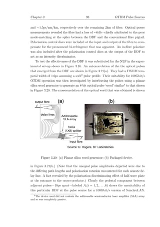
![Chapter 3 94 OTDM Pulse Sources
Figure 3.21: (a) Autocorrelation of 1.6ps pulse after DDF fibre; (b) Cross-correlation
of ’8-bit’ word. (Key: M, M : Marker bits; Ai(i = 1, 2, . . . , 6): Address bits.)
Nevertheless this pulse source was successfully used in a 100Gbit/s optical packet
header recognition experiment [50]. A representative cross-correlation of an optical
word or ’header’ from that experiment is shown in Figure 3.22. Further optimi-
Source: J. K. Lucek, BT Laboratories
(a) (b)
Figure 3.22: Word generation from ’active’ planar silica delay element. (a) Word
1;(b) Word 2.
sation of the adiabatic soliton compression process would admit the possibility of
even shorter—femtosecond domain—pulses [51] in ultrafast optical transmission and
terabit switching applications. So despite this lack of progress Section 3.3.3.1 has
described how the combination of a gain-switched DFB pulse source and a dispersion
compensating fibre can be used to produce optical pulses of the required temporal](https://image.slidesharecdn.com/a1b5bb05-a929-4e33-93de-a2dfe5b88eed-160311214335/85/thesis-113-320.jpg)
![Chapter 3 95 OTDM Pulse Sources
width for a 40Gbit/s OTDM system. The method was demonstrated successfully
by Nagatsuma et al [52]. In that demonstration a DFB gain-switched at 500MHz
produced 7ps pulses after dispersion compensation by a DCF. These were then
adiabatically compressed to 750fs, after amplification with an EDFA and spectral
filtering, using a 2km dispersion decreasing fibre (Din = 5.71 ps/nm/km, Dout =
0.84 ps/nm/km.) This confirms the validity of the approach outlined in this chapter
and is suggestive that the limiting factor in our the current implementation was
the deviation from the optimum dispersion profile of the dispersion decreasing fibre
used. Nevertheless the problem that remains is one of timing jitter and this will be
investigated in Section 3.3.5 that follows.
3.3.5 Timing Jitter impairments
The problem still remains of pulse-to-pulse timing jitter which is a particular draw-
back of the gain-switching process in DFB lasers. An example of this undesirable
effect is shown in Figure 3.23 which illustrates both timing and amplitude jitter
where the DFB SLD module used for the measurements was identical to the one
employed for the linear compression experiments described in (Section 3.3.3, p. 79).
Consequently the experimental set-up is identical to that shown in Figure 3.9 the
differences being that the repetition rate was increased to 2.5GHz—which is the
operational requirement for the OTDMA network—and the bias current was 60mA.
Finally both the impulse generator and DCF were absent. The root-mean-square
(RMS) timing jitter measured directly from the sampling oscilloscope was ∼6ps.
This jitter value is an order of magnitude too large when the specifications described
by Figure 3.7 are consulted. Optical pulses of such poor quality would produce an
irrecoverable BER penalty and error floor and are unusable in the 40Gbit/s Syn-
chroLAN network.
The physical processes that underpin the timing jitter in SLD gain-switching are
well-understood. The delay between the application of a step-like current transition
and the emission of an optical pulse by a semiconductor laser was first observed
by Konnerth and Lanza in 1964 [53]. A simple analysis [54] of Equation 3.7 and
Equation 3.8 leads to the following expression for the turn-on delay, Td, when a
step-like current pulse of the form
I(t) =
Ilow for t < 0
Ihigh for t > 0
(3.29)
is applied to a semiconductor laser diode,](https://image.slidesharecdn.com/a1b5bb05-a929-4e33-93de-a2dfe5b88eed-160311214335/85/thesis-114-320.jpg)
![Chapter 3 96 OTDM Pulse Sources
Figure 3.23: Tektronix Communication Signal Analyser trace of timing and ampli-
tide jitter for a gain-switched DFB SLD. Note asymmetry in timing jitter histogram
which indicates an RMS timing jitter of ∼5.97ps. (Horizontal scale 20ps/div, infinite
persistence enabled.)
Td = τs
Ihigh − Ilow
Ihigh − Ith
(3.30)
Here τs, is the spontaneous recombination rate, Ihigh, final current for t > 0, Ilow,
initial current for t < 0, and Ith, the threshold current. It is possible to appreciate
that any variations in Ilow will lead to variations in Td.
Td =
2τs for Ilow = 0
τs for Ilow = Ith
(3.31)
This is the mechanism behind deterministic or correlated jitter and serves to
underline the desirability of the laser returning to a steady state current before the
application of subsequent excitations because any variation in Ilow translates into
a variation of the turn-on delay. It is these variations that provide a deterministic
mechanism for turn-on jitter that is pattern dependent—i.e.dependent on the history
of the initial current, Ilow, of preceeding pulses [55].](https://image.slidesharecdn.com/a1b5bb05-a929-4e33-93de-a2dfe5b88eed-160311214335/85/thesis-115-320.jpg)
![Chapter 3 97 OTDM Pulse Sources
However an additional mechanism exists leading to turn-on jitter which is in-
dependent of bit-patterning effects. Consider the gain-switched laser diode as a
photonically discharged capacitor where the coherent “discharge” or optical pulse
is initiated by a random, spontaneous photon. Since stimulated photons have a
well defined phase, frequency, direction and polarisation that is inherited from their
antecedents, the resulting optical output is coherent. But the first stimulated pho-
ton arises from a spontaneous photon with an arbitrary phase and polarisation [56].
Below threshold only spontaneous photons are present, whilst above threshold, stim-
ulated photons dominate. So at threshold there is a phase transition from stochastic,
incoherent spontaneous emission to deterministic, coherent stimulated emission [57]
which is illustrated in Figure 3.24. It is physically manifest as a variance in the turn-
time
photondensity
stochastic deterministic
Figure 3.24: Illustration of turn-on event.
on event and is commonly termed uncorrelated timing jitter. The rate equations in
their present from, Equation 3.7 and Equation 3.8, do not account for this effect.
They can be artificially modified by including Langevin noise terms [58, 59, 60, 61]
however a comprehensive treatment requires a quantum mechanical approach [57].
This latter approach reveals that stimulated emission depends on the presence of
a finite incoherent field—in effect a spontaneous photon—at threshold to inititate
the cascade of stimulated photons that forms the gain-switched pulse. Without this
seed photon stimulated emission remains zero for all time—no matter how large the
population inversion within the laser cavity [57].
In gain-switched semiconductor lasers the uncorrelated timing jitter variation has
an asymmetric probabilty density function [62]—this is observable in the histogram](https://image.slidesharecdn.com/a1b5bb05-a929-4e33-93de-a2dfe5b88eed-160311214335/85/thesis-116-320.jpg)
![Chapter 3 98 OTDM Pulse Sources
beneath the leading edge of the waveform in Figure 3.23 which shows the output
from a DFB laser that was gain-switched at 2.5GHz. Even taking the asymmetry
into account the RMS timing jitter indicated of ∼5.97ps is far outside the required
constraints described by Figure 3.7 Weber et al. [63] numerically studied this effect
by assuming that laser emission at threshold is partially polarized and duly obtained
a similar asymmetric probability density function for turn-on delay variation. They
explained that at threshold the light output is still dominated by unpolarised spon-
taneous photons—so only spontaneous photons with the appropriate polarisation
and frequency states for the coherent field within the cavity can seed the stimulated
photon mode. It is worth pondering that if the spontaneous seeding photon was
replaced by a coherent seeding photon—with a well-defined phase—this could then
provide a means for reducing uncorrelated turn-on delay or timing jitter. This is
the method that will be considered in further detail in Section 3.6.
3.3.6 Timing Jitter measurement analysis
For measurements of uncorrelated timing jitter of less than 1ps modern sampling
oscilloscopes are unreliable. For example the four channel HP83480 mainframe used
in all experiments described in this chapter (unless otherwise indicated) had the
values given in Table 3.2 for RMS jitter measured after a fifteen minute recording
Channel number RMS timing jitter, σscope
(fs)
1 960
2 820
3 890
4 760
Table 3.2: Sampling oscilloscope channel jitter measurements.
interval. The simple deconvolution, σ2
jitter = σ2
measured − σ2
scope becomes increasingly
inaccurate as σmeasured → σscope. However a more accurate technique using RF
spectrum analysis is possible [64, 65, 66]. The basic idea is summarised in Figure 3.25
which depicts the fourier transform or power spectrum of a temporal pulse train
with both amplitude jitter and timing jitter. This can be formally represented by
the normalised power spectrum, PF (ω)
N
shown in Equation 3.32
PF (ω)
N
=
2π
T
2
k
δ(ωk) + Pamp.(ωk) + (2πk)2
Pjitter(ωk) . (3.32)](https://image.slidesharecdn.com/a1b5bb05-a929-4e33-93de-a2dfe5b88eed-160311214335/85/thesis-117-320.jpg)
![Chapter 3 99 OTDM Pulse Sources
Figure 3.25: RF spectra: Three main contributions: (1) δ functions represent the
fourier transfrom of the pulse train; (2) the amplitude noise is represented by the
horizontal dashed line; and (3) the temporal jitter is represented by the quadratic,
ω2
, term.
The first term on the RHS describes δ functions that represent the fourier transform
of a pristine pulse train devoid of both amplitude and timing jitter. The second
term describes amplitude jitter which is frequency independent. The final term
represents the temporal jitter which has a quadratic dependence on frequency via
the ω2
term. The frequency of the first (k = 1) harmonic, ω1, is simply the repetition
rate of the pulsetrain. Leep and Holm [66] have outlined a method to experimentally
determine the value of timing jitter using an RF spectrum analyser based on this
analysis. They showed that the origin of the noise continuum surrounding each
harmonic is due to amplitude jitter, σamp., and uncorreleated timing jitter, σjitter,
which can be represented by Equation 3.33
Bk =
1
ω1
ωk+1
2
ω1
ωk−1
2
ω1
σ2
amp. + σ2
jitterω2
dω = σ2
amp. + k2
+
1
12
ω2
1σ2
jitter (3.33)
Where Bk represents the relative spectral power density for each harmonic frequency,
ωk, with respect to the noise band that spans the frequency interval (ωk − 1
2
ω1, ωk +
1
2
ω1]. In this way the slope of a linear fit of experimentally determined values of Bk
against ω2
k for each harmonic yields a value for σjitter that is valid for timing jitter
values down to 200fs [66]. This is the method used later in Subsection 3.6.2.2.](https://image.slidesharecdn.com/a1b5bb05-a929-4e33-93de-a2dfe5b88eed-160311214335/85/thesis-118-320.jpg)
![Chapter 3 100 OTDM Pulse Sources
3.4 Lithium Niobate data modulation and pulse
sources
3.4.1 Lithium Niobate data modulation
The gain-switched pulse sources described in Section 3.3 produce a continuous
stream of short duration optical pulses. The most common method of transferring
data onto such an optical pulse stream utilises a pair of lithium-niobate (LiNBO3)
phase modulators [67], each of which is contained in a separate arm of an integrated
optic Mach-Zehnder interferometer [68]. The physical phenemenon underpinning
the operation of these devices is the linear electrooptical effect—the Pockels effect—
which changes the phase of the optical field within an LiNBO3 sample in response
to an applied electric field. In the Mach-Zehnder configuration the optical power
that emerges, Pout, from the integrated modulator is represented by Equation 3.34
Pout = Pin
1
2
1 − cos
V
Vπ
π (3.34)
where Pin is the power incident at the input facet of the device, V is the applied
voltage, Vπ is the voltage required to effect a π phase shift of the optical field. In
typical operation an electrical data stream or pattern with a voltage amplitude,
|V (ω)|, of Vπ, and which is synchronised to a common clock that is shared with the
optical pulse source, is combined with a DC-bias of Vbias = Vπ/2. The combined
effect serves to gate the optical pulse stream. In this way the electrical data stream
or pattern is transferred onto the optical pulse stream that emerges from the output
of the modulator. Unfortunately if the optical pulses incident to the modulator have
amplitude or timing jitter this is also transferred directly to the data modulated op-
tical pulses that emerge leading to power penalties at reception that were described
earlier in Section 3.2. A further drawback of LiNBO3 Mach-Zehnder interferometer
devices is their polarisation sensitivity although this is somewhat mitigated in inte-
grated optical versions where the polarisation state can be set and fixed provided
the intervening fibre pigtails are short.
3.4.2 Lithium Niobate optical pulse sources
The use of LiNBO3 Mach-Zehnder interferometer modulators is not confined to data
modulation. It is also possible to employ them as optical pulse sources. In this ap-
plication the device acts to periodically gate a continuous wave (CW) optical source.](https://image.slidesharecdn.com/a1b5bb05-a929-4e33-93de-a2dfe5b88eed-160311214335/85/thesis-119-320.jpg)
![Chapter 3 101 OTDM Pulse Sources
If the CW optical source is wavelength-tunable then it provides for a simple, wave-
length tunable optical pulse source that operates at flexible modulation rates within
the Er3+
window and that is readily synchronised to an elctronic clock signal at the
base rate frequency. Timing and amplitude jitter now depends only on the phase
and amplitude characteristics of the electrical drive circuitry of the clock and data
generator. In addition the chirp of these devices can be varied to order by appro-
priate DC-voltage biasing—and can be very much less than that of a gain-switched
DFB. Direct modulation of a LiNBO3 Mach-Zehnder interferometer device driven
in the manner prescribed for data modulation (i.e. |V (ω)| = Vπ, Vbias = Vπ/2)
produces pulses with a 50% duty-cycle [68] which translates into temporally broad
200ps FWHM pulses when driven at 2.5GHz. However by halving the modulating
frequency, doubling the amplitude of the drive signal and setting the DC-bias to
zero (i.e. |V (ω/2)| = 2×Vπ, Vbias = 0) the duty cycle is improved to 33% [68]. Un-
fortunately this is still too broad for the 40Gbit/s, 16 channel SynchroLAN OTDM
system system where the duty cycle required is between 1–1.5% (5–6ps at 2.5GHz
that was outlined in Section 3.2.1.) Further improvements are possible by including
overtones or harmonics of the fundamental modulation frequency. Blank [68] pre-
scribes the following optimum harmonic content—f0+0.3of3+0.15f5+0.07f7—where
the amplitudes have been normalised with respect to the modulating frequency, f0.
Unfortunately this method can at best provide pulses with an 8.3% duty cycle—still
short of the required 1%–2%. In addition the extinction ratio can be no better than
23dB whereas an RZ pulse source with an extinction ratio of ∼46dB was outlined in
Section 3.2.1 as a requirement for the pulse source. In a practical implementation
closed-loop feedback may be required to maintain the optimised drive conditions.
This adds to the complexity of the pulse source. Otherwise voltage drift of the
drive electronics or evolution of the polarisation state within the device can ad-
versely affect interferometric operation leading to a reduction in the extinction ratio
and inter-pulse amplitude “ripples” (Gibbs phenemenon) between the optical pulses.
What is required, therefore, is a compact electro-optical device with an enhanced
non-linear transfer function and an improved extinction ratio. Section 3.5 considers
such a device—the Electroabsorption Modulator.](https://image.slidesharecdn.com/a1b5bb05-a929-4e33-93de-a2dfe5b88eed-160311214335/85/thesis-120-320.jpg)
![Chapter 3 102 OTDM Pulse Sources
3.5 Electroabsorption modulator pulse sources
3.5.1 Introduction
In common with LiNBO3 modulators, the timing and amplitude jitter of Electroab-
sorption (EA) modulators depends only on the phase and amplitude characteristics
of the electrical drive circuitry of the clock and data generator. EA modulators also
have substantially lower frequency chirp when they are compared to directly modu-
lated semiconductor lasers and so are attractive for networks where low-chirp pulses
are preferred. Yet the lower chirp reduces the amount of temporal pulse compres-
sion obtainable at low repetition rates but as the driving frequency is increased the
strongly non-linear variation of device optical absorption characteristics with applied
(reverse) bias voltage enables the formation of low-duty cycle picosecond duration
pulses ultimately limited by the parasitic capacitance of the device [69]. It was shown
in Section 3.2.1 that for OTDM applications it is vital that the temporal overlap of
pedestal components from adjacent channels are suppressed to minimise the power
penalty at reception. In the case of LiNBO3 modulators short optical pulse gener-
ation at low repetition rates (<5GHz) requires the addition of harmonic frequency
components to sharpen the rise-/fall-times of the optical pulses. Similar techniques
have been used with EA modulators where either a dual-frequency or an electrical
impulse generator signal (see Figure 3.26) was used to sharpen the drive signal to
Figure 3.26: Electrical impulse generation of 12 volts, 70ps FWHM, from a step
recovery diode-voltage inverter combination at 500MHz.
the device. Both techniques have demonstrably improved the duty cycle of the gen-](https://image.slidesharecdn.com/a1b5bb05-a929-4e33-93de-a2dfe5b88eed-160311214335/85/thesis-121-320.jpg)
![Chapter 3 103 OTDM Pulse Sources
erated pulses over direct sinusoidal modulation at 2.5 GHz [70] whic is the frequency
of interest. The present Section considers the perfomance of EA modulators as opti-
cal pulse sources at several distinct modulation rates: 500MHz, 2.5GHz and 20GHz.
The former had a duty cycle of 0.7% and would be suitable for use in fine-grain,
high-speed photonic networks. Optical pulse generation at 20GHz was also inves-
tigated using a combination of linear dispersion compensation fibre and non-linear
fibre propagation to obtain additional temporal compression. Although repetition
rates as high as 30GHz with a pulsewidth of 9.48 ps have been reported [71], the
optical pulses generated at 20GHz were significantly shorter (<2ps.) Section 3.5.2
will next review the physical principles underlying the operation of EA modulators.
(Discussion of non-pulse source applications, specifically gating and demultiplexing,
will be deferred until Chapter 4 and Chapter 5.)
3.5.2 Theory
In bulk semiconductor materials at low temperatures excitonic5
effects increase and
sharpen the optical absorption near the electronic band edge which reduces the
band gap slightly. These effects are manifest as an increase in, and red-shifting of,
the optical absorption at the band edge [72]. At room temperature this effect is
suppressed because the thermal energy of the lattice is greater than the binding en-
ergy of the exciton, however restricting the physical dimensions of the bulk material
serves to enhance the excitonic effect [73, 74]. Indeed this quantum confinement
within a GaAs quantum well was found to stabilise and enhance the excitonic effect
sufficiently to make it observable at room temperature due to the increased binding
energy. The quantum confinement effect can be further enhanced by creating multi-
ple quantum well (MQW) devices obtained by alternating either different material
types, or the layer thickness of one particular material type, through the sample [75].
In 1958 Franz and Keldysh independently proposed that the application of an
electric field to a bulk semiconductor material could serve to increase the optical
absorption at the band edge [76]. The mechanism was attributed to the enhanced
tunnelling probability for a valance electron to move to the conduction band in the
presence of both an electric field and a photon with energy approaching that of the
band gap. Large shifts in band-edge absorption for electric fields perpendicular to
the MQW layers were observed that greatly exceeded (×50) the excitonic binding
energy. Miller [77] found that the application of an external electric field normal to
5
An exciton is formed by the coloumbic attraction between an electron and a hole resulting in
a hydrogen-like bound state.](https://image.slidesharecdn.com/a1b5bb05-a929-4e33-93de-a2dfe5b88eed-160311214335/85/thesis-122-320.jpg)
![Chapter 3 104 OTDM Pulse Sources
λ op wavelength
absorption E>0E=0
Figure 3.27: Application of electric field red-shifts absorption due to Quantum Con-
fined Stark Effect (QCSE.) E: Applied electric field; λop: Operational wavelength.
the MQW plane in GaAs shifted the feature to lower energies effectively decreasing
the band gap and manifest as a red-shift of absorption. The explanation of the effect
was quantum confinement in thin semiconductor layers and christened the Quantum
Confined Stark Effect (QCSE.) The excitonic (hydrogen-like bound state between an
electron and a hole) in a low dimensional material is red-shifted upon application of
an electric field Figure 3.27 which is equivalent to reducing the energy required for it
to cross the forbidden energy gap between valance and conduction bands. (Miller et
al. [76] showed that the QCSE becomes the Franz-Keldysh effect as the width of
the quantum well becomes larger in the absense of excitonic effects.) This can be
understood by referring to Figure 3.28. Quantum confinement gives rise to discrete
energy levels within the quantum wells. The minimum energy or ground state of
each well however is finite as dictated by the Heisenberg uncertainty principle [75].
With no applied electric field the band gap energy is Ea as shown in Figure 3.28(a.)
The application of an external electric field perturbs the energy band so that the
wavefunctions are distorted and displaced. The net effect is that the difference in
ground state energies is now reduced to Ea as depicted in Figure 3.28(b) where
Ea = Eg + Ec1 + Ev1 − B (3.35)
Ea < Ea (3.36)
This results in a red shift of the absorption edge. So if the material is probed by
a broadband light source an increase in absorption is observed in response to the
application of the electic field. The implication for device applications is that the](https://image.slidesharecdn.com/a1b5bb05-a929-4e33-93de-a2dfe5b88eed-160311214335/85/thesis-123-320.jpg)
![Chapter 3 105 OTDM Pulse Sources
conduction
band edge
valance
band edge
(b)(a)
n=1
n=2
n=1
n=2
n=3
n=3
Ec 1
Ev 1
Ec’ 1
Ev’ 1
E=0 E=0
Figure 3.28: Bound states in a Single Quantum Well (not to scale): (a) No electric
field E = 0; (b) Electric field appliedE = 0.
optical absorption of the material at a wavelength corresponding to the band gap
energy can be modulated in sympathy with the applied electric field. Actually there
is a reduction in the magnitude of absorption to an applied electric field for two
reasons: the reduced overlap of electron and hole wave functions and the reduction
in excitonic confinement [78].
Electroabsorption modulators are fabricated as reverse-biased PiN diodes with
the addition of MQW’s within the undoped intrinsic region. The devices are nor-
mally operated in reverse-bias so that optical absorption at the operating wave-
length, λop, is maximised (see Figure 3.27.) Application of a positive-going voltage
modulation serves to reduce the electric field corresponding to a blue-shift of the
band edge which allows light to pass through the device. The output power, Pout,
is given by Equation 3.37
Pout = Pin exp [−Γα(V )L] (3.37)
where Pin is the power incident to the input facet of the device, Γ is the confinement
factor; α(V ) is the voltage dependent absorption, and L is the device length. This
shows the trade-off between the extinction ratio ε = Pout(minimum)/Pin and the](https://image.slidesharecdn.com/a1b5bb05-a929-4e33-93de-a2dfe5b88eed-160311214335/85/thesis-124-320.jpg)
![Chapter 3 106 OTDM Pulse Sources
insertion loss of the device. The longer the device the higher the extinction ratio
which is a desirable characteristic but also the higher the insertion loss which is
less desirable. So the device geometry now becomes critical being a choice between
transverse (where light propagates perpendicular to the plane of the MQW’s) or
longitudinal (where light propagates along the plane of the MQW’s.) The latter
has been universally adopted as the geometry of choice because the longer device
length ensures a greater extinction ratio. These devices can then be cleaved to an
approriate length that represents the best compromise between extinction ratio and
insertion loss. This geometry is also more favourable for monolithic integration [78].
A drawback of longitudinal EA modulators is their tendency to have different prop-
agation constants between the TE- and TM-polarisation modes. This is mainfest
as an undesirable polarisation sensitivy [78]. Figure 3.29 shows measurements of a
Figure 3.29: (a) Polarisation sensitivity and (b) insertion loss for TE and TM modes
of a typical packaged discrete EA modulator.
device that exhibits marked polarisation sensitivity. In Figure 3.29(b) the differen-
tial loss between the TE- and the TE-modes reaches 19dB for a reverse-bias of 2.5
volts. A further limitation of early devices is that they were rated for a maximum
input power of <5dBm so as to prevent power-induced optical damage. This is a
less serious problem with LiNBO3 modulators. New polarisation insensitive devices
have become available and their use will be explicitly stated when employed in a
particular experiment or measurement in the sections that follow.](https://image.slidesharecdn.com/a1b5bb05-a929-4e33-93de-a2dfe5b88eed-160311214335/85/thesis-125-320.jpg)
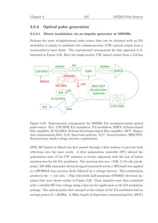


![Chapter 3 113 OTDM Pulse Sources
Figure 3.37: Dual in-line EA Modulators (a) autocorrelation; (b) spectrum for dual
in-line autocorrelators drive by 1GHz SRDs.
from Figure 3.37(b) at 0.55nm. These gave a time-bandwidth product (∆ν∆t) of
0.449 which is consistent with a transform limited gaussian pulse. The additional
EA modulator not only helps to reduce the pulsewidth over a single device but it
also serves to greatly improve the extinction ratio of the pulse source. Finally the
850fs timing jitter that was measured corresponded to the resolution limit of the
HP osciiloscope and is wholly due to the phase noise of frequency synthesiser. So
to conclude, whilst the pulsewidth was close to the requirement, the unfortunate
lack of availability of impulse generators that operated at 2.5GHz meant that the
dual-inline concatenated EA modulator approach could not be pursued at that time.
3.5.3.4 Actively mode-locked 1GHz ring laser using an EA Modulator
When an amplitude modulator (AM) is placed within a ring cavity that contains an
optical gain element mode-locking can occur when the driving frequency matches
the round-trip frequency of the laser cavity. The process can be described from
either a time- or frequency-domain point of view [79]. In the time-domain approach
a dominant, circulating optical pulse arrives at an amplitude modulator during its
period of maximum transmission—other competing pulses that circulate are blocked
by the modulator during its interval of minimum transmission and are eventually
attenuated. The frequency domain approach considers harmonics of the longitudinal
cavity modes within the bandwidth of the optical gain element as being phase-locked
to the driving frequency of the amplitude modulator. The experimental arrangement](https://image.slidesharecdn.com/a1b5bb05-a929-4e33-93de-a2dfe5b88eed-160311214335/85/thesis-132-320.jpg)

![Chapter 3 115 OTDM Pulse Sources
provide spectral broadening via self-phase modulation. A pair of optical isolators
one located before, and the other after, the SOA prevented reflections into the active
region of the SOA. A spectral filter with a bandwidth of 12nm defined the operating
wavelength of the cavity. A set of polarisation controller were used to maintain a
consistent polarisation state throughout the ring cavity. A fibre delay line adjusted
the cavity length to coincide with an integral number of cavity harmonics allowing
for mode-locking. The autocorrelation of the optical pulses that emerged via the 3dB
coupler are shown in Figure 3.40(a) where the measured FWHM pulsewidth of 17ps
Figure 3.40: Mode-locked laser at 1 GHz
corresponded to a 12ps gaussian pulse. The spectral width shown in Figure 3.40(b)
was 2.3nm. Together these gave a a time-bandwidth product (∆ν∆t = 3.43) which
is consistent with a highly chirped gaussian pulse. A dispersion compensating optical
fibre with a dispersion parameter of -4ps/nm was used to compress the pulses giving
the autocorrelation shown in Figure 3.41(a). The autocorrelation pulsewidth of 3
ps corresponding to a gaussian FWHM of 2.1 ps gave a (∆ν∆t = 0.605) which
indicates some residual chirp. The timing jitter was measured to be 615fs which
was well within the design specifications. However the absence of a closed loop
control system to adjust the cavity length to the driving frequency to maintain
mode-locking meant that as the temperature varied so too did the length of the
ring cavity which was manifest as a gradual evolution of the autocorelation to the
’Kaisers helmet’ shown in Figure 3.41(b) characteristic of partial mode-locking. The
broad pedestal corresponds to a mode-locked pulse however the central ‘spike’ is a
symptom of strong amplitude fluctuations [79]. This effect precludes its use as a](https://image.slidesharecdn.com/a1b5bb05-a929-4e33-93de-a2dfe5b88eed-160311214335/85/thesis-134-320.jpg)
![Chapter 3 116 OTDM Pulse Sources
Figure 3.41: Mode-locked ring laser @ 1GHz but with compression fibre. (b) the
main problem is absence of closed-loop control to prevent the source losing lock and
drifting.
pulse source given that the added complexity of the closed-loop control system is
not consistent with a simple, practical pulse source.
External cavity mode-locked semiconductor lasers optical provide excellent opti-
cal pulses but they require an external cavity to provide optical feedback to enable
phase locking of the longitudinal cavity modes. No such devices were available for
experimentation during the evaluation period. However commercial versions are
available but their high price tag would not lend them easily to LAN environments.
However in Section 1.3.3 of Chapter 1 their use in high-performance a CRAY vector
supercomputer was discussed [80].
3.5.3.5 High repetition rate: 20GHz optical pulse generation
A common trait of the EA Modulator approach is its flexibility and simplicity.
Bearing in mind upgrade paths for SynchroLAN at higher clock rates it was in-
structive to pursue higher repetition rate approaches. It was reported that an EA
modulator was used to produce pulses with a FWHM of 2.5ps at a repetition rate
of 15GHz using adiabatic soliton compression [81]. Guy et al. demonstrated even
shorter FWHM pulsewidths of ∼200fs duration at a repetition rate of 10GHz us-
ing an EA modulator followed by a chirped fibre grating and a DDF [82]. This
section describes the generation of pulses with duration less than 2ps FWHM at
a repetition rate of 20GHz using an EA modulator followed by a DCF and DDF.](https://image.slidesharecdn.com/a1b5bb05-a929-4e33-93de-a2dfe5b88eed-160311214335/85/thesis-135-320.jpg)
![Chapter 3 117 OTDM Pulse Sources
These pulses were suitable for OTDM systems at bit rates up to 100Gbit/s. The
experimental arrangement is illustrated in Figure 3.42. The 1560nm CW output
2km DDF
+8 -> +2
ps/nm/km
isolator PC
EAM
isolator
EDFA
6nm filter
-38ps/nm/km
100m DCF
Er:Yb-EDFA
20GHz
Pol.
CW-ECL
1560nm
PC PC
to
S/A
A/C
,
Figure 3.42: Experimental Arrangement. PC: Polarisation Controller; D: Fibre
Dispersion Parameter; DDF: Dispersion Decreasing Fibre; DCF: Dispersion Com-
pensating Fibre; EDFA: Erbium-doped Fibre Amplifier; Yb:Er-DFA: Ytterbium:
Erbium-doped Fibre Amplifier.
from a tunable external cavity semiconductor laser was incident on the packaged
EA modulator which had a static fibre-to-fibre insertion loss of ∼8–9 dB. A fibre
Polarisation Controller (PC) altered the polarisation state of the CW radiation to
ensure alignment with the axis of the EA modulator that corresponded to the lowest
insertion loss. A 10 volts peak-peak, 20 GHz sinusoidal electrical signal (measured
across a 50Ω load) superimposed upon a variable DC bias voltage was used to mod-
ulate the EA modulator. The fabrication and structure of the EA modulator has
been described in detail by Moodie et al. [83, 84]. The resulting stream of optical
pulses was amplified with an Erbium-Doped Fibre Amplifier (EDFA) followed by a
6nm (3dB width) optical filter to reduce the amplified spontaneous emission noise
intensity. At the filter output the mean optical power was measured to be ∼3dBm.
A 100m length of non-soliton supporting DCF with a chromatic dispersion param-
eter of -38ps/nm/km was then used to compensate for the frequency chirp imposed
on the optical pulses by the EA modulator. (Section 3.3.4.1 described how initially
chirped pulses which are used to form solitons can give rise to undesirable dispersive
waves [44].) A Erbium:Ytterbium-doped fibre amplifier (Er:Yb-DFA) boosted the
mean optical power of the pulses before launch into the soliton supporting DDF that
was described earlier in Section 3.3.4.2. A fibre polariser was incorporated at the](https://image.slidesharecdn.com/a1b5bb05-a929-4e33-93de-a2dfe5b88eed-160311214335/85/thesis-136-320.jpg)
![Chapter 3 118 OTDM Pulse Sources
output of the DDF and suppressed low-level pedestal components generated dur-
ing the pulse formation process [85]. Temporal pulse profiles were observed using
a background-free autocorrelator. An optical spectrum analyser with a resolution
of 0.1nm recorded the corresponding spectral features. Transform-limited pulses as
short as 4.1ps at 20GHz were obtained using this EA modulator when followed by
linear pulse compression in the DCF [83]. In the measurements, an applied DC
reverse-bias voltage of 7 volts gave rise to a pulsewidth of 7.2ps measured at the
output of the EA modulator Figure 3.43(b.) The corresponding time-bandwidth
product ∆ν∆t was calculated to be 0.45 (assuming a chirped hyperbolic secant
squared pulse.) After linear pulse compression in the DCF the pulsewidth reduced
to 5.1ps with ∆ν∆t = 0.31 for a hyperbolic secant squared pulseshape. These,
transform-limited pulses, were then launched into the DDF via the Er:Yb-DFA. As
the power of the optical pulse train to the DDF was increased there was a corre-
sponding decrease of the pulsewidth at the output due to soliton compression in the
DDF, as shown in Figure 3.43(a) and (b) (circles.) For the maximum launch power
Figure 3.43: Pulsewidth (assuming a hyperbolic secant squared pulse) as a function
of power launched into Dispersion Decreasing Fibre. (a) 10GHz; (b) 20GHz rep-
etition rate. The arrow in (b) corresponds to autocorrelation and spectral plot in
Figure 3.44. (Dashed spline curve to guide eye.)
of +19.4dBm, a pulse width of 1.9ps was recorded. It is depicted in Figure 3.44(a.)
The corresponding optical spectrum is depicted in Figure 3.44(b.) The FWHM of
the optical spectrum was 1.5nm resulting in ∆ν∆t = 0.35. Adjustment of the PC
before the polarizer aided discrimination between the soliton and pedestal consistent](https://image.slidesharecdn.com/a1b5bb05-a929-4e33-93de-a2dfe5b88eed-160311214335/85/thesis-137-320.jpg)
![Chapter 3 119 OTDM Pulse Sources
Figure 3.44: (a) Autocorrelation and (b) corresponding spectral plot at 20 GHz
repetition rate. Launched power to DDF: 19.4dBm.
with the mechanism of non-linear polarisation rotation [86]. However, despite care-
ful optimisation, a small pedestal component remained. The cause of this pedestal
was consistent with other observations of DDF pulse compression where a propor-
tion of the pulse energy was contained within the pedestal component [87]. This
approach underlines the flexibility of EA modulator-based pulse sources in terms of
repetition rates and upgrade paths to higher linerates.
3.6 Hybrid (GS-DFB & EAM) pulse source
3.6.1 Introduction
Earlier in this chapter (Page 95 in Section 3.3.5,) it was described how gain-switching
could readily produce short, return-to-zero (RZ) optical pulses of the required duty
cycle from a compact, bit-rate flexible, semiconductor laser diode via direct electri-
cal modulation synchronised to a network clock. The main drawback of the method
was that the temporally-asymmetric pulses suffered from unacceptable timing jitter
(recall Figure 3.23) which is a major concern as it impairs the interleaving process.
This, in turn, would lead to the BER penalties upon reception that were outlined in
Section 3.2.2.2 and in Reference [88]. It is possible to reduce, but not eliminate, the
timing jitter of gain-switched semiconductor lasers by biasing above threshold, but
at the expense of increased inter-pulse pedestal and multi-pulse relaxation oscilla-](https://image.slidesharecdn.com/a1b5bb05-a929-4e33-93de-a2dfe5b88eed-160311214335/85/thesis-138-320.jpg)
![Chapter 3 120 OTDM Pulse Sources
tions which have an adverse impact on the system penalty. It was also described how
external modulation of a CW source by either a LiNBO3 or EA modulator could
likewise produce short, RZ optical pulses at flexible bit-rates by direct electrical
modulation once again synchronised to the network clock. The main drawback was
that this technique suffered from a poor duty-cycle—being too broad temporally.
That said, it was suggested in Section 3.5.3.2 and Section 3.5.3.3 that the use of
2.5GHz impulse generators might, if they had been available to drive an EA modu-
lator, have made for the ideal, low-jitter, low-pedestal, low duty-cycle pulse source
required for SynchroLAN.
It is also possible to reduce the timing jitter of gain-switched semiconductor
laser diodes by making use of light injection into the laser cavity. Two methods are
of note. The first method is self-seeding which involves reflecting a portion of the
gain-switched pulse back into the laser cavity to be coincident with the formation of
subsequent gain-switched pulses. This has been shown to reduce timing jitter [89].
However, it depends quite critically on matching the repetition rate to the external
cavity length. But it requires mechanical adjustment of the external reflective el-
ement which would prove unwieldy and inappropriate for a low-maintenance pulse
source. The second method is to use the external injection of CW coherent light. An
approach that has the advantage of being bit-rate independent provided that an ap-
propriate injection wavelength is chosen that is within the gain-switched spectrum.
(This will be addressed in Section 3.6.2.2 to follow.) The technique has demon-
strably been shown to reduce the timing jitter of the optical pulses generated by
gain-switched Fabry-Perot (FP) semiconductor laser diodes [63, 89, 90]. It is worth
emphasising that gain-switched DFBs are more susceptible to timing jitter when
compared to gain-switched Fabry-Perot SLD’s [63]. The drawback of the technique
is that whilst this method produces excellent low-jitter optical pulses [91, 92] it is
at the expense of an increased pulse pedestal [92].
Recall that Section 3.5.3 described how EA Modulators could be used to mod-
ulate a CW optical signal by virtue of their non-linear absorptive response to an
externally applied voltage. But it need not be a CW optical signal—the synthesis
of gain-switching and electroabsorption modulation where the chirped pulses from
a gain-switched DFB-SLD laser diode were temporally filtered or gated with an EA
Modulator to reduce pulse width variation was demonstrated by Guy [93]. How-
ever since timing jitter is still present the non-square switching window of the EA
Modulator converts timing jitter into amplitude jitter. In addition the random ar-
rival of the jittered, frequency chirped pulses with respect to the synchronous gating](https://image.slidesharecdn.com/a1b5bb05-a929-4e33-93de-a2dfe5b88eed-160311214335/85/thesis-139-320.jpg)
![Chapter 3 121 OTDM Pulse Sources
window opened by the EA Modulator is converted into a wavelength jitter. This
wavelength jitter can then be re-converted to timing jitter arising from chromatic
dispersion during propagation leading to power penalties in an OTDM system af-
ter demultiplexing at the receiver. What is required then is a hybrid pulse source
that leverages the best features of both approaches—namely CW injection to sup-
press the timing jitter of the optical pulses coupled with synchronous gating of the
resulting low-jitter pulses to remove the attendant inter-pulse pedestal.
3.6.2 Optical pulse generation
To investigate this approach further the experimental arrangement outlined in Fig-
ure 3.45 was constructed. A 2.5GHz electrical sine wave generated by a HP 83620A
GS-DFB CW-DFBPC
FILTER
PC PC
EDFA
PC
~ 60mA
2.5GHz 12.5GHz
~ -3 volts
NDF
FILTER
EAM
4 3
21
Figure 3.45: Experimental setup. GS-DFB: gain-switched distributed feedback
semiconductor laser diode; CW-ECL: continuous wave external cavity laser; PC:
polarisation controller; EDFA: Erbium-doped fibre amplifier; DCF: dispersion com-
pensating fibre.Note: ‘1,’ ‘2,’ ‘3’ and ‘4’ refer to the port number of the fused-fibre
coupler.
frequency synthesiser was amplified and combined with an adjustable DC bias cur-
rent (via a bias-tee) to enable gain switching of a DFB-SLD contained within a
high-speed package. The DFB-SLD used was a ridge-waveguide device [94, 95]
with a centre wavelength of ∼1547nm and threshold current of 39mA at 15◦
C. The
DFB-SLD temperature and DC-bias current were maintained at 15◦
C and 60mA,
respectively, throughout the measurements. The electrical signal to the packaged](https://image.slidesharecdn.com/a1b5bb05-a929-4e33-93de-a2dfe5b88eed-160311214335/85/thesis-140-320.jpg)
![Chapter 3 122 OTDM Pulse Sources
device was transported over SMA cabling and had a peak-to-peak voltage of ∼10
volts measured across a 50Ω load. The optical pulse stream that resulted had a
mean optical power of -3dBm and was injected into the top arm of a 50/50 coupler,
denoted port 1 in Figure 3.45.
A wavelength tunable, HP 8168A external-cavity laser (ECL) optical source in-
jected coherent light through port 2 into the cavity of the gain-switched DFB-SLD
having first passed through an optical isolator and a 50/50 coupler. A set of con-
trollers was used to alter the polarisation state of the injected light before it entered
the cavity of the DFB-SLD. Port 4 was used to monitor the power and wavelength of
the CW light. The gain-switched pulses which exited port 3 were filtered by a 1.1nm
bandpass filter to remove spectral extremities and suppress the non-linear chirp be-
fore injection into an Erbium-doped Fibre Amplifier (EDFA) that boosted the power
applied to the input of the EA Modulator to +4dBm (the maximum recommended
incident power to the device.) The EA Modulator employed an InGaAsP/InGaAsP
multiple quantum well absorber layer. The low capacitance buried ridge structure
was a modification of that previously described [83]. It comprised an 0.8µm wide
active mesa encased in a 5µm thick Fe-doped InP blocking structure. The EA Mod-
ulator chip was 370µm long and was fully packaged in a high speed connectorised
fibre-pigtailed module. At 1550nm the fibre-to-fibre insertion loss of the module
was 7.3dB, its modulation depth was 30.4dB and its 3dB electrical bandwidth was
14GHz. The EA Modulator was driven by a 12.5GHz electrical sine wave gener-
ated by a separate HP 83623A frequency synthesiser, that was phase-locked to the
2.5GHz synthesiser, and amplified to 11 volts (peak-to-peak into 50Ω.) The separate
driving frequency was required because at 2.5GHz the EA Modulator switching win-
dow at ∼60–70ps is clearly too broad to effectively remove the pedestal. However
when driven with a 12.5GHz signal the switching window was reduced to ∼20ps
which proved ideal. In practice every fifth cycle of the 12.5GHz signal (1
5
×12.5 GHz
= 2.5GHz) was temporally coincident with the peak of the 2.5GHz gain-switched
pulses. An adjustable microwave delay line allowed translation of the EA Modula-
tor switching window with respect to the low-jitter gain-switched pulses. The pulses
that emerged from the EA Modulator were compressed with a negatively dispersive
optical fibre (D = 13ps/nm.)
3.6.2.1 Timing jitter reduction
Figure 3.46 shows the sampling oscilloscope traces that demonstrate the beneficial
effect of CW light injection in suppressing the temporal jitter of the gain-switched](https://image.slidesharecdn.com/a1b5bb05-a929-4e33-93de-a2dfe5b88eed-160311214335/85/thesis-141-320.jpg)
![Chapter 3 123 OTDM Pulse Sources
Figure 3.46: High-speed sampling oscilloscope traces: (a) CW light injection off, (b)
CW light injection on.
optical pulses. Figure 3.46(a) was recorded with the oscilloscope persistence facility
enabled and in the absence of CW light injection. It portrays the reduced pulse
definition typical of timing jitter. Figure 3.46(b) records the dramatic change that
occurs when the coherent CW injection from the ECL is present. It also indicates
that coherent CW light injection advanced the turn-on of the gain-switched pulses
by ∼15-20 ps. To quantify the amount of jitter reduction Figure 3.47 shows the RF
spectra obtained with: (a) CW light injection absent and (b) CW light injection
present. In the latter case the injected power was -8.4dBm at 1547.6nm. (The back-
ground noise-floor where no optical power was incident to the RF spectrum analyser
is indicated by the dashed line common to Figure 3.47(a) and Figure 3.47(b).) The
reduction of the phase noise background due to uncorrelated timing jitter with CW
light injection is evident when Figure 3.47(a) is compared to Figure 3.47(b). The
values for temporal jitter were extracted using the method proposed by Leep and
Holm [66] and outlined earlier on Page 98 in Section 3.3.6. These are plotted in
Figure 3.48 and revealed an URTJ of 3.6ps without CW light injection, in Fig-
ure 3.48(a), and 0.6ps with CW light injection, in Figure 3.48(b). In a subsequent
experiment the coherent CW light was maintained at a constant power of -2dBm,
whilst the ECL was stepped in wavelength across the gain-switched spectral profile
(dashed line in Figure 3.49(a).) For each step in wavelength the uncorrelated root-
mean-square timeing jitter (URTJ) was recorded. As the wavelength was discretely
discretely the jitter decreased until a plateau region of width ∼1nm was entered](https://image.slidesharecdn.com/a1b5bb05-a929-4e33-93de-a2dfe5b88eed-160311214335/85/thesis-142-320.jpg)

![Chapter 3 125 OTDM Pulse Sources
Figure 3.48: Calculation of jitter: (a) plot used to calculate URTJ, CW off, (b) plot
used to calculate URTJ, CW on.
tions displayed in Figure 3.50(a) and Figure 3.50(b) indicate the dramatic pedestal
suppression obtained. The pedestal-suppressed pulses had a temporal Full-width
Half-maximum (FWHM) of 4.0ps (assuming a sech2
profile) and a spectral FWHM
of 1.1nm after passage through the normally dispersive fibre giving a time-bandwidth
product ∆ν∆t of 0.56. The pedestal extinction was in excess of 25dB (measurement
limited by the photomultiplier noise floor of the autocorrelator.) EA Modulator’s
with modulation depths in excess of 40dB are now available [96]. To better illus-
trate this improvement pulses were divided equally between the two output arms
of a passive fused-fibre coupler. One arm was made sufficiently long and included
a variable optical delay to ensure that upon recombination by a second fused-fibre
coupler the Nth
and N − 25th
pulses emerged separated by 25ps (40GHz.). The
resulting cross correlations of the interleaved pulses, 25ps apart, are shown in Fig-
ure 3.51. Seo et al. have reported [92] that CW light injection reduced the timing
jitter but broadened the pulses in gain-switched DFBs. This effect was also observed
but, in addition, the broadened pulses were accompanied by an increased inter-pulse
pedestal Figure 3.51(a) and Figure 3.51(b). The benefit of using the EA Modula-
tor as a temporal gate to effectively remove this inter-pulse pedestal is apparent in
Figure 3.51(c). This immediately suggested the suitability of these pulses for the 40
Gbit/s OTDM SynchroLAN system.
The remaining problem of non-linearly chirped components within the gain-
switched pulses is conventionally addressed by spectral filtering, yet as can be ap-](https://image.slidesharecdn.com/a1b5bb05-a929-4e33-93de-a2dfe5b88eed-160311214335/85/thesis-144-320.jpg)

![Chapter 3 127 OTDM Pulse Sources
Figure 3.50: Autocorrelations with CW light injection: (a) EA modulator off; (b)
EA Modulator on.
light injection might allow jitter-free, zero-bias gain-switching. This is very desirable
because a bias-free DFB would remove the need for optical monitoring and feedback
control of the bias point and have reduced power consumption and be particularly
suitable for optical interconnect applications [62, 97]. Wang et al. [98], have demon-
strated that CW light injection increases the resonance frequency of semiconductor
laser diodes. Hence CW light injection can usefully extend the maximum modu-
lation frequency and in this fashion reduce or eliminate the detrimental effects of
bit-patterning where the duration, profile and temporal postion of an optical pulse is
determined by its antecedents [97, 99]. These, along with the other benefits outlined
already: low-jitter (temporal and spectral) and low-pedestal provide for a practical
pulse source for OTDM and associated applications.
3.7 Summary and conclusions
This chapter was primarily concerned with the specification and performance of sev-
eral optical pulse source alternatives for the 40Gbit/s SynchroLAN OTDMA system.
The constraints that each potential pulse source was subject to, for example multi-
plexer/demultiplexer impairments, timing jitter and extinction ratio, were presented
and formed a set of criteria against which the candidate devices were evaluated. It
must also be borne in mind that the limited-space and economic constraints inherent
in commercial LANs precludes expensive, “perfectly-engineered,” solutions.](https://image.slidesharecdn.com/a1b5bb05-a929-4e33-93de-a2dfe5b88eed-160311214335/85/thesis-146-320.jpg)

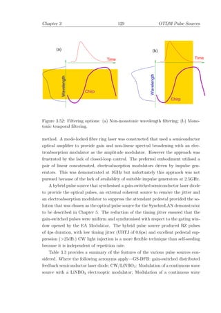
![Chapter 3 130 OTDM Pulse Sources
2.5GHz 12.5GHz
DC-biasDC-bias
CW DFB GS DFB EAM CW DFB GS DFB EAM
(b)(a)
2.5GHz
IG IG
Figure 3.53: Alternative configurations: (a) In-line configuration; (b) Impulse gen-
erators further simplify set-up.
Pulse Source Complexity Duty cycle Extinction ratio Jitter
GS-DFB Medium Good Poor High
CW/LiNBO3 Low poor Good Very low
CW/EA Modulator Low poor Very good Very low
CW/Dual EA Modulator Medium Very Good Excellent Very low
ML-FRL Very High Excellent Excellent Low, but drift
Hybrid High Excellent Excellent Very low
Table 3.3: Classification and properties of the various pulse sources described in this
chapter.
source with a single electroabsorption modulator; CW/Dual EA Modulator: Mod-
ulation of a continuous wave source with a pair of electroabsorption modulators;
ML-FR: mode-locked fibre ring laser incorporating a semiconductor optical amplifier
and an electroabsorption modulator; Hybrid Source: The preferred source incorpo-
rating a gain-switched semiconductor laser diode, an external coherent source and
an electroabsorption modulator
The work of this Chapter has been the subject of several publications [42, 100,
101]. Indeed the hybrid pulse source was deemed sufficiently novel to be wor-
thy of patent protection [102]. The knowledge acquired in gain-switching and
non-linear pulse compression one involving contributed directly to the success of
several related inititiatives including all-optical packet routing and switching at
100Gbit/s [50, 103, 104, 105] In these cases the jitter was not an issue since for
packet switching pulses that comprised each 8-bit optical header were derived from](https://image.slidesharecdn.com/a1b5bb05-a929-4e33-93de-a2dfe5b88eed-160311214335/85/thesis-149-320.jpg)
![Chapter 3 131 OTDM Pulse Sources
CW-DFB
Circulator
GS-DFB
EAM
Circulator
Fibre Grating
Figure 3.54: Alternative in-line arrangement of components.
a single pulse and therefore not subject to inter-header pulse jitter but rather intra-
header jitter. The self-synchronising nature of the switching node accomodated the
asynchronous arrival (or jitter) of packets. The techniques were also applied to
soliton experiments at 1.3µm [106, 107].](https://image.slidesharecdn.com/a1b5bb05-a929-4e33-93de-a2dfe5b88eed-160311214335/85/thesis-150-320.jpg)
![Bibliography
[1] A. D. Ellis, All optical networking beyond 10Gbit/s: OTDM Networks based
on electro-optic modulators and fibre ring lasers. Ph.D. thesis, University of
Aston in Birmingham, April 1997.
[2] M. Jinno, “Effects of crosstalk and timing jitter on all-optical time-division
demultiplexing using a nonlinear fibre Sagnac interferometer switch,” IEEE J.
Quantum Electron., vol. 30, no. 12, pp. 2842–2853, December 1994.
[3] K. Y. Lau, “Short-pulse and high-frequency signal generation in semiconductor
lasers,” IEEE J. Lightwave Technol., vol. LT-7, pp. 400–419, February 1989.
[4] V. D. Kurnasov, V. I. Magalyas, A. A. Pleshkov, L. A. Rivlin, V. G. Trukhan,
and V. V. Tsvetkov, “Self modulation of emission from an injection semicon-
ductor laser,” JETP Lett., vol. 4, pp. 303–305, December 1966.
[5] R. Roldan, “Spikes in the light output of room temperature GaAs junction
lasers,” Appl. Phys. Lett., vol. 11, pp. 346–349, December 1967.
[6] S. Tarucha and K. Otsuka, “Response of semiconductor laser to deep sinusoidal
injection current modulation,” IEEE J. Quantum Electron., vol. 17, pp. 810–
816, May 1981.
[7] J. AuYeung, “Picosecond optical pulse generation at gigahertz rate by direct
modulation of a semiconductor laser,” Appl. Phys. Lett., vol. 38, no. 5, pp. 308–
310, March 1981.
[8] J. P. Van der Ziel and R. A. Logan, “Generation of short optical pulses by
combined dc and microwave current injection,” IEEE J. Quantum Electron.,
vol. QE-18, pp. 1340–1350, September 1982.
132](https://image.slidesharecdn.com/a1b5bb05-a929-4e33-93de-a2dfe5b88eed-160311214335/85/thesis-151-320.jpg)
![Chapter 3 133 BIBLIOGRAPHY
[9] P. M. Downey, J. E. Bowers, R. S. Tucker, and E. Agyekum, “Picosecond
dynamics of a gain-switched InGaAsP laser,” IEEE J. Quantum Electron.,
vol. QE-23, pp. 1039–1046, June 1987.
[10] N. Onodera, H. Ito, and H. Inaba, “Fourier-transform-limited single-mode
picosecond optical pulse generation by a distributed feedback laser,” Appl.
Phys. Lett., vol. 45, pp. 843–845, October 1984.
[11] D. H. Auston, “Picosecond nonlinear optics,” in Ultrafast Light Pulses: Pi-
cosecond Techniquies and Applications (S. L. Shapiro, ed.), vol. 18 of Topics
in Applied Physics, ch. 4, pp. 186–190, Berlin: Springer-Verlag, 1977.
[12] J. L. Moll and S. A. Hamilton, “Physical modelling of the step-recovery diode
for pulse and harmonic generation,” Proc. IEEE, vol. 57, no. 7, pp. 1250–1259,
July 1969.
[13] M. R. T. Tan, S. T. Wang, D. E. Mars, and J. L. Moll, “12ps GaAs double
heterostructure step recovery diode,” Electron. Lett., vol. 28, no. 7, pp. 673–
675, March 1992.
[14] P. Torphammar and S. T. Eng, “Picosecond pulse generation in semiconductor
lasers using resonance oscillation,” Electron. Lett., vol. 16, no. 15, pp. 587–589,
July 1980.
[15] C. Lin, P. L. Liu, T. C. Damen, D. J. Eilenberger, and R. L. Hartman, “Sim-
ple picosecond pulse generation scheme for injection lasers,” Electron. Lett.,
vol. 16, no. 15, pp. 600–602, July 1980.
[16] D. Botez, “Analytical approximation of the radiation confinement factor for
the TE0 mode of a double heterojunction laser,” IEEE J. Quantum Electron.,
vol. QE-14, no. 4, pp. 230–232, April 1977.
[17] C. H. Henry, “Theory of the linewidth of semiconductor lasers,” IEEE J.
Quantum Electron., vol. QE-18, pp. 259–264, February 1982.
[18] M. Liu, “Direct modulation,” in Principles and applications of optical com-
munications, ch. 12, pp. 591–638, Chicago: Irwin, 1 ed., 1996.
[19] I. H. White, “Picosecond optical pulse generation using semiconductor lasers,”
in Laser Sources and Applications: Proceedings of the 47th Scottish Universi-
ties Summer School in Physics (A. Miller and D. M. Finlayson, eds.), NATO](https://image.slidesharecdn.com/a1b5bb05-a929-4e33-93de-a2dfe5b88eed-160311214335/85/thesis-152-320.jpg)
![Chapter 3 134 BIBLIOGRAPHY
Advanced Study Institute, ch. 13, pp. 63–84, Bristol and Philadelphia: Insti-
tute of Physics, 1996.
[20] R. J. Helkey and Y. Arakawa, “Cavity optimization for minimum pulsewidth
of gain-switched semiconductor lasers,” IEEE Photon. Technol. Lett., vol. 7,
pp. 272–274, March 1995.
[21] H. Kogelnik and C. V. Shank, “Stimulated emission in a periodic structure,”
Appl. Phys. Lett., vol. 18, no. 4, pp. 152–154, February 1971.
[22] L. D. Westbrook, “Dispersion of linewidth-broadening factor in 1.5µm laser
diodes,” Electron. Lett., vol. 21, no. 22, pp. 1018–1019, October 1985.
[23] S. Ogita, M. Yano, and H. Imai, “Theoretical calculation of the linewidth
enhancement factor of DFB lasers,” Electron. Lett., vol. 22, no. 11, pp. 580–
581, May 1986.
[24] C. A. Green, N. K. Dutta, and W. Watson, “Linewidth enhancement factor
in InGaAsP/InP multiple quantum well lasers,” Appl. Phys. Lett., vol. 50,
no. 20, pp. 1409–1410, May 1987.
[25] G. P. Agrawal, “Optical sources and transmitters,” in Fiber-Optic Communi-
cation Systems (K. Chang, ed.), Wiley series in microwave and optical engi-
neering, ch. 3, pp. 75–135, New York: Wiley, 1 ed., 1992.
[26] M. Osi´nski and M. J. Adams, “Picosecond pulse analysis of gain-switched
1.55µm InGaAsP lisers,” IEEE J. Quantum Electron., vol. QE-21, no. 12,
pp. 1929–1936, December 1985.
[27] L. Chusseau, “Propagation of single-mode 1.5µm gain-switched semiconductor
laser pulses in normally dispersive fibers,” IEEE J. Quantum Electron., vol. 30,
pp. 2711–2720, November 1994.
[28] H. Itoh, S. Sudo, K. Okamoto, and T. Hosaka, “Optical pulse compression
in 1.5µm wavelength region using large-positive-dispersion fibre and grating
pair,” Electron. Lett., vol. 24, no. 13, pp. 785–786, June 1988.
[29] K. O. Hill, Y. Fujii, D. C. Johnson, and B. S. Kawasaki, “Photosensitivity
in optical fiber waveguides: Application to reflection filter fabrication,” Appl.
Phys. Lett., vol. 32, no. 10, pp. 647–649, May 1978.](https://image.slidesharecdn.com/a1b5bb05-a929-4e33-93de-a2dfe5b88eed-160311214335/85/thesis-153-320.jpg)
![Chapter 3 135 BIBLIOGRAPHY
[30] C. R. Giles, “Lightwave applications of fiber Bragg gratings,” J. Lightwave
Technol., vol. 15, no. 8, pp. 1391–1404, August 1997.
[31] F. Ouellette, “Dispersion cancellation using linearly filtered Bragg grating
filters in optical waveguides,” Opt. Lett., vol. 12, no. 10, pp. 847–849, October
1987.
[32] R. Kashyap, “Design of step-chirped fibre gratings,” Opt. Commun., vol. 136,
no. 3, pp. 461–469, April 1997.
[33] P. L. Mason, R. V. Penty, and I. H. White, “Extending the transmission
distance of a directly modulated laser source using bragg grating dispersion
compensators,” IEE Colloquium on ’Optical Fibre Grating and Their Appli-
cations’, vol. 1, no. 1, pp. 9/1–9/6, January 1995.
[34] P. L. Mason, R. V. Penty, and I. H. White, “Increasing the transmission
distance of a directly modulated laser with a chirped fibre bragg grating dis-
persion compensator,” Electron. Lett., vol. 31, no. 4, pp. 281–282, February
1995.
[35] P. L. Mason, R. V. Penty, and I. H. White, “Multiple stage dispersion compen-
sation in long haul optical fibre systems using chirped fibre gratings,” Electron.
Lett., vol. 30, no. 15, pp. 1244–1245, February 1995.
[36] B. J. Eggleton, P. A. Krug, L. Poladian, K. A. Ahmed, and H. F. Liu, “Exper-
imental demonstration of compression of dispersed optical pulses by reflection
from self-chirped optical fiber bragg gratings,” Optics Letters, vol. 12, no. 34,
pp. 877–879, 1994.
[37] K. A. Ahmed, H. F. Liu, P. A. Krug, and F. Ouellette, “Simultaneous mode
selection and pulse compression of gain-switched pulses from a fabry-perot
laser using a 40-mm chirped optical fiber grating,” IEEE Photon. Technol.
Lett., vol. 7, pp. 158–160, 1995.
[38] R. Kashyap, P. F. McKee, R. J. Campbell, and D. L. Williams, “A novel
method of producing all fibre photo-induced chirped gratings,” Electron. Lett.,
vol. 30, no. 12, pp. 996–997, 1994.
[39] K. Ennser, R. I. Laming, M. N. Zervas, M. Ibsen, and M. Durkin, “Effects
of non-ideal group delay and reflection characteristics of chirped fibre grating
dispersion compensators,” Proc. ECOC ’97, vol. 2, pp. 45–48, September 1997.](https://image.slidesharecdn.com/a1b5bb05-a929-4e33-93de-a2dfe5b88eed-160311214335/85/thesis-154-320.jpg)
![Chapter 3 136 BIBLIOGRAPHY
[40] D. Garthe, G. Milner, and Y. Cai, “System performance of broadband dis-
persion compensating gratings,” Electron. Lett., vol. 34, no. 6, pp. 582–583,
March 1998.
[41] R. Kashyap and M. de Lacerda Rocha, “On the group delay characteristics of
chirped fibre Bragg gratings,” Opt. Comm., vol. 153, pp. 19–22, July 1998.
[42] P. Gunning, R. Kashyap, A. S. Siddiqui, and K. Smith, “Picosecond pulse
generation of <5ps from a gain-switched DFB semiconductor laser diode using
a linearly step-chirped fibre grating,” Electron. Lett., vol. 31, no. 13, pp. 1066–
1067, 1995.
[43] S. A. Planas, N. L. Pires Mansur, C. H. Brito Cruz, and H. L. Fragnito, “Spec-
tral narrowing in the propagation of chirped pulses in single-mode fibers,” Opt.
Lett., vol. 18, no. 9, pp. 699–701, May 1993.
[44] C. Desem and P. L. Chu, “Effect of chirping on soliton propagation in single-
mode optical fibres,” Opt. Lett., vol. 11, no. 4, pp. 248–250, 1986.
[45] M. N. Islam, C. E. Soccolich, J. Gordon, and U. C. Paek, “Soliton intensiy-
dependent polarisation rotation,” Opt. Lett., vol. 15, pp. 21–23, January 1990.
[46] P. V. Mamyshev and S. V. Chernikov, “Generation of fundamental soliton
trains for high-bit-rate optical fiber communications,” IEEE J. Quantum Elec-
tron., vol. QE-27, pp. 2347–2355, March October 1991.
[47] V. A. Bogatyrev, M. M. Bubnov, E. M. Dianov, A. S. Kurkov, P. V. Mamy-
shev, A. M. Prokorov, S. D. Rumyantsev, S. L. Semenov, A. A. Sysoliatin, S. V.
Chernikov, A. N. Gur’yanov, G. G. Devyatykh, and S. I. Miroshnichenko, “A
single-mode fiber with chromatic dispersion varying along the length,” IEEE
J. Lightwave Technol., vol. 9, no. 5, pp. 561–566, May 1991.
[48] S. V. Chernikov, D. J. Richardson, R. I. Laming, D. M. Dianov, and D. N.
Payne, “70 Gbit/s fibre based source of fundamental solitons at 1550nm,”
Electron. Lett., vol. 28, no. 13, pp. 1210–1212, 1992.
[49] M. deLacerda Rocha. Private Communication, BT Laboratories, August 1995.
[50] D. Cotter, J. K. Lucek, M. Shabeer, D. C. Rogers, D. Nesset, and P. Gunning,
“Self-routing of 100Gbit/s packets using 6-bit ‘keyword’ address recognition,”
Electron. Lett., vol. 31, no. 25, pp. 2201–2202, December 1995.](https://image.slidesharecdn.com/a1b5bb05-a929-4e33-93de-a2dfe5b88eed-160311214335/85/thesis-155-320.jpg)
![Chapter 3 137 BIBLIOGRAPHY
[51] S. V. Chernikov and P. V. Mamyshev, “Femtosecond soliton propagation in
fibers with slowly decreasing dispersion,” J. Opt. Soc Am. B, vol. 8, no. 8,
pp. 1633–1641, 1991.
[52] T. Nagatsuma, M. Yaita, M. Shinagawa, K. Kato, A. Kozen, K. Iwatsuki,
and K. Suzuki, “Electro-optic characterisation of ultrafast photodetectors us-
ing adiabatically compressed soliton pulses,” Electron. Lett., vol. 30, no. 10,
pp. 814–816, May 1994.
[53] K. Konnerth and C. Lanza, “Delay betwen current pulse and light emission
of a Gallium Arsenide injection laser,” Appl. Phys. Lett., vol. 4, pp. 120–121,
April 1964.
[54] W. Van Etten and J. van der Platts, Fundamentals of Optical Fiber Communi-
cations. International Series in Optoelectronics, London: Prentice-Hall, 1 ed.,
1991.
[55] T. M. Shen, “Timing jitter in semiconductor lasers under pseudorandom
word modulation,” IEEE J. Lightwave Technol., vol. 7, no. 9, pp. 1394–1399,
September 1989.
[56] R. Loudon, The quantum theory of light. Oxford: Oxford University Press,
2nd ed., 1983.
[57] L. Mandel and E. Wolf, Optical coherence and quantum optics. Cambridge:
Cambridge University Press, 1st ed., 1995.
[58] D. Marcuse, “Computer simulation of laser fluctuations: Theory of single-
cavity laser,” IEEE J. Quantum Electron., vol. QE-20, pp. 1139–1148, October
1984.
[59] N. Schunk and K. Petermann, “Numerical analysis of the feedback regimes for
a single-mode semiconductor laser with external feedback,” IEEE J. Quantum
Electron., vol. 24, pp. 1242–1247, July 1988.
[60] A. Mecozzi, S. Piazzolla, A. D’Ottavi, and P. Spano, “Passage time statistics
in laser turn on,” Phys. Rev. A, vol. 38, no. 6, pp. 3136–3138, September 1988.
[61] E. Sano, M. Shinagawa, and R. Takahashi, “Theoretical analysis of timing
jitter gain-switched semiconductor lasers,” Appl. Phys. Lett., vol. 55, pp. 522–
524, August 1989.](https://image.slidesharecdn.com/a1b5bb05-a929-4e33-93de-a2dfe5b88eed-160311214335/85/thesis-156-320.jpg)
![Chapter 3 138 BIBLIOGRAPHY
[62] K. Obermann, S. Kindt, and K. Petermann, “Turn-on jitter in zero-biased
single-mode semiconductor lisers,” IEEE Photon. Technol. Lett., vol. 8, no. 1,
pp. 31–33, January 1996.
[63] A. G. Weber, W. Rongham, E. Hoilger B¨ottcher, M. Schell, and D. Bim-
berg, “Measurement and simulation of the turn-on delay and time jitter in
gain-switched semiconductor lasers,” IEEE J. Quantum Electron., vol. QE-
28, pp. 441–446, February 1992.
[64] D. von der Linde, “Characterization of the noise in continuously operating
mode-locked sources,” Appl. Phys. B, vol. 39, pp. 201–217, 1986.
[65] A. Finch, X. Zhu, P. N. Kean, and W. Sibbet, “Noise characterisation of mode-
locked color-center laser sources,” IEEE J. Quantum Electron., vol. QE-26,
pp. 1115–1123, June 1990.
[66] D. A. Leep and D. A. Holm, “Spectral measurement of timing jitter in gain-
switched semiconductor lasers,” Appl. Phys. Lett., vol. 60, no. 20, pp. 2451–
2453, 1992.
[67] R. C. Alferness, “Waveguide electrooptic modulators,” IEEE Trans. Mi-
crowave Theory Tech., vol. MTT-30, no. 8, pp. 1121–1137, August 1982.
[68] L. C. Blank, High capacity optical fibre transmission systems. Ph.D. thesis,
University of Wales in Bangor, August 1992.
[69] D. G. Moodie, “Electroabsorprion modulators and their impact on future
telecommunications networks,” M.Sc. thesis, University College London,
November 1994.
[70] N. M. Froberg, G. Raybon, A. M. Johnson, Y. K. Chen, T. Tanbun-Ek, R. A.
Logan, A. Tate, A. M. Sargent, K. Wecht, and P. F. Sciortino, “Pulse gener-
ation by harmonic modulation of an integrated DBR laser-modulator,” Elec-
tron. Lett., vol. 30, no. 8, pp. 650–651, April 1994.
[71] E. Yamada, K. Wakita, and M. Nakazawa, “30GHz pulse train generation
from a multiquantum well electroabsorption intensity modulator,” Electron.
Lett., vol. 29, no. 10, pp. 845–847, 1993.
[72] B. K. Ridley, Quantum processes in semiconductors. Oxford: Oxford Science
Publications, 3rd ed., 1993.](https://image.slidesharecdn.com/a1b5bb05-a929-4e33-93de-a2dfe5b88eed-160311214335/85/thesis-157-320.jpg)
![Chapter 3 139 BIBLIOGRAPHY
[73] R. Dingle, W. Wiegmann, and C. H. Henry, “Quantum states of confined car-
riers in very thin AlxGa1−xAs-GaAs-AlxGa1−x heterostructures,” Phys. Rev.
Lett., vol. 33, pp. 827–830, September 1974.
[74] J. R. Hook and H. E. Hall, “Low-dimensional systems,” in Solid State Physics
(F. Mandel, R. J. Ellison, and D. J. Sandiford, eds.), The Manchester Physics
Series, ch. 14, pp. 399–416, Chichester: John Wiley & Sons, 2 ed., 1991.
[75] T. H. Wood, “Multiple quantum well (MQW) waveguide modulators,” J.
Lightwave Technol., vol. LT-6, pp. 743–757, June 1988.
[76] D. A. B. Miller, D. S. Chemla, and S. Schmitt-Rink, “Relation between elec-
troabsorption in bulk semiconductors and in quantum wells: The quantum
confined Franz-Keldysh effect,” Phys. Rev. B., vol. 33, pp. 6976–6982, May
1984.
[77] D. A. B. Miller, D. S. Chemla, T. C. Damen, A. C. Gossard, W. Wiegmann,
T. H. Wood, and C. A. Burrus, “Band edge electroabsorption in quantum
well structures: The quantum confined stark effect,” Phys. Rev. Lett., vol. 53,
pp. 2173–2176, November 1984.
[78] J. S. Weiner, D. A. B. Miller, D. S. Chemla, T. C. Damen, C. A. Burrus,
T. H. Wood, A. C. Gossard, and W. Wiegmann, “Strong polarisation-sensitive
electroabsorption in GaAs/AlGaAs quantum well waveguides,” Appl. Phys.
Lett., vol. 47, pp. 1148–1150, December 1985.
[79] A. E. Siegman, “Active laser mode coupling,” in Lasers, ch. 27, pp. 1041–1103,
Mill Valley, CA: University Science Books, 1986.
[80] M. D. Bausman and V. Swanson, “Optical clock distribution system,” US
Patent, no. 5,537,498, Filed March 5, 1993; Assigned July 16, 1996.
[81] K. Suzuki, K. Iwatsuki, S. Nishi, M. Saruwatari, K. Sato, and K. Wakita,
“2.5ps soliton pulse generation at 15GHz with monolithically integrated
MQW-DFB-LD/MQW-EA modulator and dispersion decreasing fibre,” Elec-
tron. Lett., vol. 29, no. 19, pp. 1713–1714, 1993.
[82] M. J. Guy, S. V. Chernikov, J. R. Taylor, D. G. Moodie, and R. Kashyap,
“200fs soliton pulse generation at 10GHz through nonlinear compression
of transform-limited pulses from an electroabsorption modulator,” Electron.
Lett., vol. 31, no. 9, pp. 741–742, 1995.](https://image.slidesharecdn.com/a1b5bb05-a929-4e33-93de-a2dfe5b88eed-160311214335/85/thesis-158-320.jpg)
![Chapter 3 140 BIBLIOGRAPHY
[83] D. G. Moodie, A. D. Ellis, A. R. Thurlow, M. J. Harlow, I. F. Lealman,
S. D. Perrin, L. J. Rivers, and M. J. Robertson, “Multiple quantum well
electroabsorption modulators for 80Gbit/s OTDM systems,” Electron. Lett.,
vol. 31, no. 16, pp. 1370–1371, 1995.
[84] D. G. Moodie, A. D. Ellis, and C. W. Ford, “Generation of 6.3ps optical pulses
at a 10GHz repetition rate using a packaged electroabsorption modulator and
dispersion compensating fibre,” Electron. Lett., vol. 30, no. 20, pp. 1700–1701,
1994.
[85] B. Thedrez, H. Takeshita, and T. Kamiya, “Improved compression of InGaAsP
gain-switched DFB laser pulses using polarisation dispersion effects,” IEEE
Sixth Intl. Conf. on InP and related materials, pp. 488–491, March 1994.
[86] R. H. Stolen, J. Botineau, and A. Ashkin, “Intensity discrimination of optical
pulses with birefringent fibres,” Optics Lett., vol. 7, pp. 512–514, 1982.
[87] M. D. Pelusi and H. F. Liu, “Higher order soliton pulse compression in
dispersion-decreasing optical fibres,” IEEE J. Quantum Electron., vol. 33,
no. 8, pp. 1430–1439, August 1997.
[88] G. P. Agrawal, “Optical detectors and receivers,” in Fiber-Optic Communica-
tion Systems (K. Chang, ed.), Wiley series in microwave and optical engineer-
ing, ch. 4, pp. 174–176, New York: Wiley, 1 ed., 1992.
[89] D. Huhse, W. Schell, J. Utz, J. Kaessner, and D. Bimberg, “Generation of
low jitter (210fs) single mode pulses from a 1.3µm Fabry-Perot laser diode by
self-seeding,” Proc. ECOC ’94, vol. 1, pp. 467–470, September 1994.
[90] M. Jinno, “Correlated and uncorrelated timing jitter in gain-switched laser
diodes,” IEEE Photon. Technol. Lett., vol. 5, no. 11, pp. 1140–1143, October
1993.
[91] L. P. Barry, P. Guignard, J. Debeau, R. Boittin, and M. Bernard, “A high
speed broadcast and select TDMA network using all-optical demultiplexing,”
Proc. ECOC ’95, vol. 1, pp. 437–440, 1995.
[92] D. S. Seo, D. Y. Kim, and H. F. Liu, “Timing jitter reduction of gain-switched
DFB laser by external injection seeding,” Electron. Lett., vol. 32, no. 1, pp. 44–
45, January 1996.](https://image.slidesharecdn.com/a1b5bb05-a929-4e33-93de-a2dfe5b88eed-160311214335/85/thesis-159-320.jpg)
![Chapter 3 141 BIBLIOGRAPHY
[93] M. J. Guy, S. V. Chernikov, J. R. Taylor, D. G. Moodie, and R. Kashyap,
“Low repetition rate master source for optical processing in ultrahigh-speed
OTDM networks,” Electron. Lett., vol. 31, no. 20, pp. 1767–1769, 1995.
[94] A. W. Nelson, L. D. Westbrook, and P. J. Fiddyment, “Design and fabrica-
tion of 1.5µm ridge waveguide distributed feedback lasers,” IEE Proc. Pt. J,
vol. 132, no. 1, pp. 12–19, February 1985.
[95] L. D. Westbrook, A. W. Nelson, P. J. Fiddyment, and J. S. Evans, “Contin-
uous wave operation of 1.5µm distributed-feedback ridge-waveguide lasers,”
Electron. Lett., vol. 20, no. 6, pp. 225–226, 1984.
[96] D. G. Moodie, M. J. Harlow, M. J. Guy, S. D. Perrin, C. W. Ford, and M. J.
Robertson, “Discrete electroabsorption modulators with enhanced modulation
depth,” IEEE J. Lightwave. Technol., vol. LT-14, no. 9, pp. 2035–2043, 1996.
[97] N. K. Dutta, “Power penalty due to timing jitter for lasers modulated without
prebias,” Appl. Phys. Lett., vol. 67, pp. 3230–3232, November 1995.
[98] J. Wang, M. K. Haldar, L. Li, and F. V. C. Mendis, “Enhancement of modu-
lation bandwidth of laser diodes by injection locking,” IEEE Photon. Technol.
Lett., vol. 8, pp. 34–36, January 1996.
[99] C. Mirasso, P. Colet, and M. San Miguel, “Dependence of timing jitter on bias
level for single-mode semiconductor lasers under high speed operation,” IEEE
J. Quantum Electron., vol. QE-29, pp. 23–32, January 1987.
[100] P. Gunning, J. K. Lucek, D. G. Moodie, K. Smith, R. P. Davey, S. V.
Chernikov, M. J. Guy, J. R. Taylor, and A. S. Siddiqui, “CW injected, low-
jitter, low-pedestal, gain-switched DFB-SLD/Electroabsorption modulator-
based pulse source at 1.5µm for ultrafast network applications,” Proc. IEE
Colloquium on High Speed and Long Distance Optical Transmission, pp. 8–
1—8–6, April 18, 1996.
[101] P. Gunning, J. K. Lucek, D. G. Moodie, K. Smith, R. P. Davey, S. V.
Chernikov, M. J. Guy, J. R. Taylor, and A. S. Siddiqui, “Gain-switched DFB
laser diode pulse source using continuous wave light injection for jitter suppres-
sion and an electroabsorption modulator for pedestal suppression,” Electron.
Lett., vol. 32, no. 11, pp. 1010–1011, 1996.](https://image.slidesharecdn.com/a1b5bb05-a929-4e33-93de-a2dfe5b88eed-160311214335/85/thesis-160-320.jpg)
![Chapter 3 142 BIBLIOGRAPHY
[102] P. Gunning, R. Davey, D. G. Moodie, K. Smith, J. Lucek, and D. Nesset,
“Optical pulse source,” US Patent, no. 5,778,015, Filed May 16, 1996; Assigned
July 7, 1998.
[103] D. Cotter, J. K. Lucek, M. Shabeer, K. Smith, D. C. Rogers, P. Gunning, and
D. Nesset, “100Gbit/s packet self-routing using all-optical 6-bit ‘keyword’ ad-
dress recognition,” Proc. 21st Eur. Conf.on Opt. Comm., ECOC ‘95, Septem-
ber 1995.
[104] D. Cotter, M. C. Tatham, J. K. Lucek, M. Shabeer, K. Smith, D. C. Rogers,
D. Nesset, and P. Gunning, “Photonic address-header recognition and self-
routing in ultrafast packet networks,” IEEE/OSA 1996 International Topical
Meeting on Photonics in Switching, 21–25 April 1996.
[105] D. Cotter, M. C. Tatham, J. K. Lucek, M. Shabeer, K. Smith, D. Nesset,
D. C. Rogers, and P. Gunning, “Ultrafast all-optical signal processing for
packet switching,” Proc. 1996 International workshop on photonic network
technologies, September 1996.
[106] R. P. Davey, K. Smith, R. Wyatt, D. L. Williams, M. J. Holmes, D. M. Pataca,
M. L. Rocha, and P. Gunning, “Subpicosecond pulse generation from a 1.3µm
DFB laser gain-switched at 1GHz,” Electron. Lett., vol. 32, no. 4, pp. 349–351,
February 1996.
[107] D. M. Pataca, M. L. Rocha, R. P. Davey, K. Smith, R. Wyatt, and P. Gun-
ning, “Transmission of 5 ps solitons at 1.32µm over 50 km of standard fibre
using praseodymium doped fluoride fibre amplifiers,” Electron. Lett., vol. 32,
no. 8, pp. 754–755, April 1996.](https://image.slidesharecdn.com/a1b5bb05-a929-4e33-93de-a2dfe5b88eed-160311214335/85/thesis-161-320.jpg)

![Chapter 4 144 OTDM channel selection
data channels spaced 23.6ps apart (which corresponded to an aggregate capacity of
> 40Gbit/s) error-free and with low-power power penalty. The chapter will also
consider the use of an integrated Mach-Zehnder interferometer (IMZI) as a demul-
tiplexer. This is particularly interesting as it admits the possibility of all-optical
channel selection which will be an important function within all-optical networks.
4.2 Electroabsorption modulator channel selection
4.2.1 Background
The physical principles of electroabsorption in semiconductors have been outlined
in Section 3.5.2 of Chapter 3. In addition to the demonstrated ability of EA mod-
ulators as optical pulse sources (see Section 3.5 of Chapter 4,) they have been used
very effectively as demultiplexers. The strongly non-linear dependence of optical
absorption with applied (reverse) bias voltage typical of an EA modulator particu-
larly lends itself to the requirements for a short-switching window [1]. For example,
Marcenac et al. [2] have demonstrated demultiplexing from 80Gbit/s to 10Gbit/s.
Whilst Moodie et al. have extended this with an assessment of demultiplexing from
160Gbit/s to 20Gbit/s [3]. Within a three-node OTDM network they have been
employed very effectively to generate a periodic switching window for gating (or
dropping) a single 10Gbit/s data channel from a 40Gbit/s OTDM signal [4]. How-
ever in OTDMA networks where finer granularity (for example the selection of a
2.5Gbit/s channel from a 40 Gbit/s OTDM data stream) is required, a direct si-
nusoidal drive signal applied to the EA modulator at the channel rate may not be
suitable because the temporal width of the switching window—which is inversely
proportional to the electrical driving frequency—is still too broad. Recent demon-
strations [5, 6] have tackled this problem by using variations of the dual-frequency
technique of Froberg et al. [7]. However in the former case [5] this necessitated the
use of two frequency synthesisers, whilst in the latter case [6], additional complexity
in the form of frequency doublers and a variable phase delay. A potentially serious
drawback of these techniques arises from the additional structure that may appear
outside the main switching window from the 10f [5] and 4f [6] frequency compo-
nents, should the phase between the frequency components be misalligned. Now if
these temporal ‘side-lobes’ coincide with other channels, then partial demultiplexing
of other channels leading to undesirable crosstalk would result. One answer is to use
impulse generators [7] (see Page 77) which can transform a sinusoidal input signal](https://image.slidesharecdn.com/a1b5bb05-a929-4e33-93de-a2dfe5b88eed-160311214335/85/thesis-163-320.jpg)


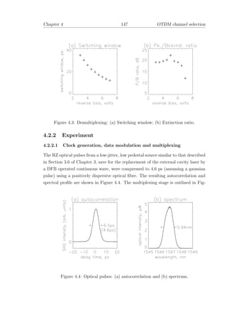
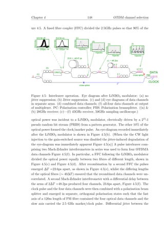

![Chapter 4 150 OTDM channel selection
Figure 4.7: Response of Impulse generator/voltage inverter combination to recovered
2.5GHz clock signal.
4.2.2.3 Specification of EA modulator
The EA modulator employed an InGaAsP/InGaAsP multiple quantum well ab-
sorber layer within a low capacitance ridged deeply etched buried ridge structure.
It comprised a 0.8um wide active mesa encased in a 5µm thick Fe-doped InP block-
ing structure. The modulator was 370µm long and was fully packaged in a high
speed connectorised fibre-pigtailed module. At 1550nm the fibre-to-fibre insertion
loss of the module was 8dB, its modulation depth was 40dB and its 3dB electrical
bandwidth was 14GHz. Further details of similar devices are contained in [1].The
data channels were amplified with an Erbium-doped fibre amplifier (EDFA) that
was connected to the input of the EA modulator. Suitable adjustment of the elec-
trical phase delay by the PS located prior to the EA modulator was then used to
selectbetween any one of the four data channels.
4.2.2.4 Results
Figure 4.8(a)—(d) shows each individual channel as displayed on a 50GHz sampling
oscilloscope using a 45GHz p-i-n photodiode. (The additional structure following
the main pulse was due to “ringing” by the photodiode.) In this case a DC-bias of -5
volts was applied to the EA modulator via the impulse generator. Adjustment of the
phase-delay of the received sinusoid allowed switching between the four channels.
Figure 4.9 shows the BER curve obtained for channel 3. No evidence for a noise](https://image.slidesharecdn.com/a1b5bb05-a929-4e33-93de-a2dfe5b88eed-160311214335/85/thesis-169-320.jpg)
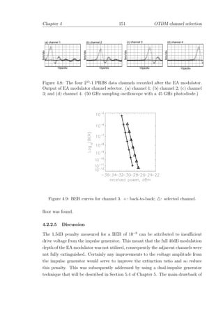
![Chapter 4 152 OTDM channel selection
the present approach arises from the polarisation dependence of the EA modulators.
This required the use of polarisation maintaining (PM) components and polarisation
controllers within the system. In a real system this is not desirable as it would require
active monitoring and control of the polarisation state of the data pulses incident
to the EA modulator. Additional crosstalk would arise from poorly executed fusion
splices and together both would become more pronounced as the component count
increased and the propagation path became longer. The answer was the use of
low-polarisation sensitivity EA modulators which will be described in Section 5.4 of
Chapter 5 and which were not available at the time the experiment was performed.
Whereas the use of EA modulators as demultiplexers requires an optoelectronic
conversion stage, Section 4.3 which follows considers an all-optical technique based
on an integrated Mach-Zehnder interferometer.
4.3 Integrated Mach-Zehnder demultiplexer
4.3.1 Background
Section 4.2 described how an electrical impulse derived from an optical clock signal
was applied to an EA modulator opening a synchronous gating window to effect
OTDM channel selection [6, 8]. This Section will describe how the same func-
tion was performed all-optically without recourse to optoelectronic conversion. The
device used was an integrated Mach-Zehnder interferometer (IMZI) [9, 10]. This
opens the way to compact, all-optical serial processing devices operating at bit
rates ∼100Gbit/s—beyond what is currently thought possible with high-speed elec-
tronics.
4.3.1.1 Interferometer fundamentals
Interferometers can convert a phase change between two coherent electric fields into
an amplitude change. Consider the generic 2×2 Mach-Zehnder interferometer shown
in Figure 4.3.1.1 where it is assumed that the coupling ratios are 50:50 (balanced)
and the device contains two, phase adjustable, elements that can independently
advance (or retard) the phase of the coherent fields within the arms by φ1 and φ2
respectively. If coherent light from port 0 is divided equally by the first coupler
between the top and bottom arms and coherently recombined at the second coupler
to emerge from port 1 and port 2 then the output power given by Equation 4.1
P1 = P0 cos2
∆Φ/2 (4.1)](https://image.slidesharecdn.com/a1b5bb05-a929-4e33-93de-a2dfe5b88eed-160311214335/85/thesis-171-320.jpg)
![Chapter 4 153 OTDM channel selection
P0 ∆Φ/2cos2
P0
P0 ∆Φ/2sin2
∆Φ = φ − φ1 2
φ
φ
1
2 =
=
P2
P1
50:50 Fused fibre couplers
port 0
port 3 port 2
port 1
Phase elements
Figure 4.10: Mach-Zehnder interferometer
and Equation 4.2 [11],
P2 = P0 sin2
∆Φ/2 (4.2)
depends on the differential phase shift, ∆Φ, between the two coherent waves, Equa-
tion 4.3,
∆Φ = φ1 − φ2 + c (4.3)
where c is a constant. Assuming that c = 0 and with ∆Φ = 0 all the power emerges
from port 1, alternatively if ∆Φ = π all the power is switched to port 2. Any time-
varying physical effect that induces a phase change to either or both phase elements
(φ1(t), φ2(t)) will be converted to a time-varying amplitude modulation (P1(t), P2(t))
at the output ports. Dynamic switching of the optical power exclusively from one
port to the other port can be achieved when ∆Φ : 0 → π or ∆Φ : π → 0.
4.3.1.2 Switching speed and figures of merit
If the device is required to switch high speed optical signals it is necessary to im-
press the phase change on the order of several hundred femtoseconds (fs). Clearly
mechanical, temperature or pressure effects cannot produce a response at this speed,
however for high optical intensities many non-linear optical materials display inten-
sity dependent phase changes due to the induced change in refractive index mediated
by χ(3)
[12] that can. This was introduced as the Kerr effect expressed as Equa-
tion 4.4 in Chapter 2.
n = n0 + n2I (4.4)
As before n0 is the linear refractive index, I is the optical intensity, and n2 is the Kerr
coefficient. The magnitude of the Kerr coefficient varies from material to material.
At first glance it would appear that the larger the Kerr coefficient the more suitable](https://image.slidesharecdn.com/a1b5bb05-a929-4e33-93de-a2dfe5b88eed-160311214335/85/thesis-172-320.jpg)
![Chapter 4 154 OTDM channel selection
the material for non-linear optical switching. However in practice this is offset by the
material absorption, α, and the speed of response/recovery of the non-linearity, τ.
A useful figure of merit, FOM, which bundles these together was given by Vogel [13],
and is reproduced in Equation 4.5,
FOM =
n2
ατ
(4.5)
(Note τ is the response time of the non-linearity or 1 ps, whichever is the largest.)
Table 4.1 [13] ranks three separate material systems which possess a Kerr non-
Material n2(m2
/W) α(cm−1
) FOM
MQW, GaAs/GaAlAs 10−8
103
102
Polydiacetylenes 10−15
10 104
Glass 10−18
10−2
105
Table 4.1: Non-linear optical properties and figure of merit of several material sys-
tems.
linearity. On this evidence glass emerges as the best candidate. For an optical fibre
the phase shift due to self- and cross-phase modulation is given by Equation 4.6 [14]
φ(τ) = k0n2L [ISPM
(τ) + 2IXPM
(τ)] (4.6)
Where k0 is the transverse mode propagation constant, L the interaction length,
and ISPM
(τ) the pulse intensity for self-phase modulation (SPM,) and IXPM
(τ) the
intensity for cross phase modulation (XPM.) Glass does have one drawback and that
is the long interaction length (several km’s) required to achieve a π phase change.
In the Mach-Zehnder configuration long lengths of optical fibre are sensitive to
environmental effects which induce differential phase drifts between the arms that is
manifest as noise and instability. These effects can be reduced if the Sagnac geometry
is used instead, giving rise to the non-linear optical loop mirror (NOLM) which uses
a single coupler and a single, looped, fibre arm [15]. However ∼0.6W of peak power
is required to obtain a π phase shift for a loop length of ∼1km [16]. In addition
both MZI and NOLM configurations require an imbalance or asymmetry to effect
the differential phase shift. This can be achieved through SPM by using a slightly
asymmetric coupling ratio but at the expense of a reduction in the extinction ratio.
Alternatively XPM can be induced by injecting ‘control’ pulses at a wavelength
different from the signal into one arm in the case of a MZI; or unidirectionally into
the loop in the case of a NOLM.](https://image.slidesharecdn.com/a1b5bb05-a929-4e33-93de-a2dfe5b88eed-160311214335/85/thesis-173-320.jpg)
![Chapter 4 155 OTDM channel selection
4.3.1.3 Semiconductor optical amplifiers
Semiconductor optical amplifiers were introduced in Section 2.2.6.2 of Chapter 2. At
first glance it would appear from Table 4.1 that multi-quantum well GaAs/GaAlAs—
one commonly used material systems used for semiconductor optical amplifiers—is
a poor material for switching purposes because of the high absorption. However the
table takes no account of the gain available which can overcome the loss. Moreover in
earlier chapters it was shown that modulation of the gain either optically or by elec-
tronic injection, can induce phase changes or chirping. In particular the effective n2
for a typical semiconductor optical amplifier (SOA) is ∼ 1×10⁻⁹
cm2
/W [17] which is
several orders of magnitude larger than that for Silica Fibre ∼ 3.2×10⁻¹⁶
cm2
/W [18]
consequently,
∆nSOA
∼ 107
∆nF IBRE
(4.7)
In the particular case of a saturated SOA, the first term of Equation 4.6 can be
re-expressed as Equation 4.8 [17]
φ(τ) =
α
2
gτc
¯hω0
I(τ) (4.8)
here α, is the linewidth enhancement factor, g, is the gain coefficient, τc is the carrier
lifetime and ¯hω0 is the photon energy. In the SLALOM [19] configuration, the SOA
is displaced from the mid-point of the fibre loop. An input pulse is divided by the
coupler into clockwise and counterclockwise travelling pulses that arrive at the SOA
at different times. If the clockwise pulse is the first to pass through the unsaturated
SOA and depletes the gain, then the counterclockwise pulse encounters a saturated
SOA. When both pulses recombine at the coupler having traversed the loop they have
accumulated a differential phase shift. With suitable adjustment of the SOA current,
loop polarisation or pulse power the NOLM can behave either transparently or as a
mirror. The terahertz optical asymmetric demultiplexer (TOAD) is a refinement of
the SLALOM where the differential saturation is induced by a strong control pulse
that is injected into the loop and acts to saturate the SOA. The differential phase
shift can be induced if the control pulse is injected to arrive just after the clockwise
signal pulse has emerged from the SOA, but before the counter clockwise signal
pulse enters the device. Gain saturation is a fast process, but gain recovery is slow.
So before the process can be repeated, time must be allowed for the saturated gain
to relax sufficiently to recover a π phase change. This relaxation time ultimately
limits the repetition rate at which the SOA can switch.](https://image.slidesharecdn.com/a1b5bb05-a929-4e33-93de-a2dfe5b88eed-160311214335/85/thesis-174-320.jpg)
![Chapter 4 156 OTDM channel selection
4.3.1.4 Heinrich-Hertz IMZI Device construction
The InGaAsP/InP material system of SOAs is readily integratable and the com-
pact sizes possible are less affected by environmental effects such as temperature
compared to NOLMs. An integrated Mach-Zehnder interferometer (IMZI) device,
typical of the one shown in Figure 4.11 was provided by HHI1
. Complete details of
Source: E. Jahn & N. Agrawal, HHI Berlin.
port 2port 3
port 0 port 1
Figure 4.11: Typical HHI unpackaged IMZI device.
the method of fabrication, structure and characteristics are described by Jahn [20].
Briefly, the 2×2 InGaAsP/InP-based device measuring 4×2mm consisted of two 3-
dB multi-mode-interference (MMI) couplers with two semiconductor optical ampli-
fiers (SOAs) integrated within its branches. The bulk InGaAsP SOAs, butt-coupled
to passive waveguide sections were fabricated in an etched mesa buried heterostruc-
ture geometry with semi-insulating Fe:InP blocking layers. The centres of the two
SOAs were displaced longitudinally by 300µm, which, in the contra-propagating ge-
ometry, led to a switching window width of ∼8ps [21]. At BT Labs the device was
bonded into a purpose made stainless steel sub-module to facilitate the attachment
of four single-mode, lensed fibre sub-assemblies. Each fibre sub-assembly consisted
of a single-mode lensed fibre sealed into a stainless steel tube by solder glass. These
sub-assemblies were independently aligned and then laser welded to the sub-module
to obtain optimum coupling efficiency and stable alignment of the four waveguides
of the IMZI. The sub-module containing the IMZI complete with the four welded
sub-assemblies, was placed on a peltier cooler and enclosed in an aluminium box [22]
1
Heinrich-Hertz-Institut f¨ur Nachrichtentechnik, Berlin, Germany](https://image.slidesharecdn.com/a1b5bb05-a929-4e33-93de-a2dfe5b88eed-160311214335/85/thesis-175-320.jpg)

![Chapter 4 158 OTDM channel selection
4.3.2.2 Switching window and gain recovery
The temporal width of the switching window is determined by the differential spatial
offset between the amplifiers and the temporal width of the control pulse. (The lat-
ter because of the integrating nature of the non-linearity.) The temporal width of the
switching window was measured by a simple pump-probe measurement where CW
light @ 1563nm was injected to saturate each SOA, whilst a 4ps FWHM, repetitive
(2.5GHz) probe pulse at 1548nm was injected contradirectionally. The output, as
monitored on a high speed (45GHz) p-i-n photodetector, is shown in Figure 4.13(a).
The sudden dip in the optical power corresponded to the fast gain depletion initi-
400psamp 1amp. 2
7.6 ps
Max. Transmission
Min. Transmission
Max. Transmission
Min. Transmission
(a) (b)
Figure 4.13: Switching window of HHI IMZI: (a) Gain recovery; (b) switching win-
dow.
ated by the probe pulse and was followed by the much slower gain recovery. After
400ps the process is repeated. The width of the switching window can be deter-
mined by closer examination of the moment of gain depletion which is shown in
Figure 4.13(b). The temporal offset between the minima of for each separate SOA
was 7.6ps. Although the gain recovery time is slow the differential recovery is not.
This is because the differential phase of π is only available within the interval imme-
diately after gain recovery commences within the first SOA and before gain recovery
of the second SOA. For the SOA to switch again, a phase shift of π must be recovered
which sets an upper limit to the maximum speed at which the device can operate.
However the rate of recovery can be increased by injection of a CW holding beam
at a wavelength different to that of either pump or probe beams [23]. In that study
the gain recovery, normally ∼130 ps (7–8GHz) with the holding beam disabled, was
reduced to ∼12.5ps (80GHz) with the holding beam enabled.
The gain recovery effect was investigated with the IMZI device. The geometry
and optical configuration for the measurements are shown in Figure 4.14, which, for
clarity, does not contain the circulator and isolators that were orientated appropri-](https://image.slidesharecdn.com/a1b5bb05-a929-4e33-93de-a2dfe5b88eed-160311214335/85/thesis-177-320.jpg)

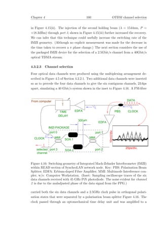
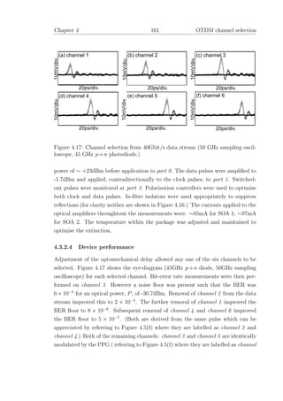
![Chapter 4 162 OTDM channel selection
1 and channel 3.) Surprisingly when the clock pulse was removed an improvement
of 4.6dB to the penalty was obtained for the same BER of 5 × 10⁻⁷
. This was sug-
gestive of some clock dependent effect. To investigate this further the data pulses
were removed and only the clock pulse was incident to the device. Clear evidence of
reflection effects were apparent when port 3 was monitored for various combinations
of the SOA currents shown in Figure 4.18: (i) Both SOA’s off; (ii) SOA 1 on; (iii)
SOA 2 on; (iv) SOA 1 & SOA 2 on. One particular reflection effect was observed by
1mV/div.
50ps/div.
1
2 3 4
5
6 7
8 9 10
11 12
13
14
15
16
(iii) SOA 2 on
(ii) SOA 1 on
(i) Both SOAs off
(iv) SOA 1 & SOA 2 on
Figure 4.18: Reflections: (i) Both SOA’s off; (ii) SOA 1 on; (iii) SOA 2 on; (iv) SOA
1 & SOA 2 on.
re-applying the data pulses, having first adjusted the polarisation state so that port
3 produced the unswitched output displayed in Figure 4.19. The degradation to
channels ∼100ps behind the switched-out channel was apparent Figure 4.19(a)–(d).
This adverse effect persisted as the clock pulse was translated. It can be appreciated
then that some of this energy would be present within the sampling window of the
selected channel contributing to the BER noise floor.
4.3.2.5 Discussion
The reflections at the acrtive/passive interfaces were a fundamental limitation to
the demultiplexing performance of the particular device used. These conspired to
coherently add each high intensity clock pulse to the selected data channel. However
similar IMZI devices from HHI have displayed much better performance in demul-
tiplexing a 40Gbit/s OTDM data stream to 5Gbit/s [9, 20] which sugests that the
particular device used may poorly represent the quality of the HHI devices. The
spatial offset between the SOAs fix the temporal width of the switching window.](https://image.slidesharecdn.com/a1b5bb05-a929-4e33-93de-a2dfe5b88eed-160311214335/85/thesis-181-320.jpg)
![Chapter 4 163 OTDM channel selection
10mV/div.
20ps/div.
(a) channel 1
10mV/div.
(b) channel 2
20ps/div. 20ps/div.
10mV/div.
(c) channel 310mV/div.
(d) channel 4
20ps/div.
10mV/div.
(e) channel 5
20ps/div.
10mV/div.
20ps/div.
(f) channel 6
Figure 4.19: Indirect evidence of reflected clock leakage into data channels. For
example (a) channel 1 switched-out, interference effect 100ps behind in Channel
4; (b) channel 2 switched-out, interference effect 100ps behind in Channel 5; (c)
channel 3 switched-out, interference effect 100ps behind in Channel 6.
More flexible designs that allow the clock pulse to be applied separately to each SOA
allow the width of the switching window to be defined externally and allow for op-
eration at different bit-rates. [24]. The inclusion of adjustable phase shifters within
each arm, separate from the SOAs, permits an extra degree of freedom when trim-
ming the differential phase between the two SOAs. This is particularly relevant to
asymmetric configurations [24]. Despite the particular problems encountered with
the packaged IMZI, more recent experiments have demonstrated 80 to 10Gbit/s
demultiplexing of an OTDM pulse stream [25], whilst Diez et al. [26] from HHI
have shown multiwavelength, 8 × 80 Gbit/s → 8 × 10 Gbit/s error-free demulti-
plexing. Polarisation-insensitive, all-optical 3R regeneration has been demonstrated
at 20Gbit/s by Jepson et al. [27] using a monolithically integrated Michelson inter-
ferometer. These demonstrations underline the tremendous potential of all-optical
interferometric devices within ultrafast photonic networks.
4.4 Conclusions
The present chapter described demultiplexing from an OTDM data stream with
two devices: EA modulators and integrated Mach-Zehnder interferometers. EA
modulators driven by electrical pulses from an impulse generator and derived from
a separate, distributed optical clock were used to select a 2.5 Gbit/s data channel](https://image.slidesharecdn.com/a1b5bb05-a929-4e33-93de-a2dfe5b88eed-160311214335/85/thesis-182-320.jpg)
![Chapter 4 164 OTDM channel selection
from a 40 Gbit/s OTDM data stream. Channel selection was achieved by varying the
phase delay of the optoelectronically received network clock before application to the
impulse generator. The EA modulator as a demultiplexer represents a potentially
cheap, generic technology with the possibility for monolithic integration. However a
drawback of EA modulator demultiplexing is the finite static insertion loss of ≥10dB
which may require amplification before reception in some circumstances.
An integrated Mach-Zehnder interferometer provided an all-optical method of
channel selection that allowed the distributed optical clock to interact directly with
the data channels using the nonlinearity in a pair of semiconductor laser amplifier
within the arms of the device. The integrated nature of the IMZI device is attractive
because of its compact dimensions. The attraction of this approach is that the clock
signal does not not require optoelectronic conversion, as was the case with the EA
modulator, and so it can be used directly for channel selection. This is a desirable
function in an all-optical network because it allows data to remain in optical form
between the source and destination nodes. Channel selection was achieved using a
slow, (1s) programmable electromechanical optical delay line which served to vary
the arrival time of the clock pulse to the SOAs. Although channel selection was
demonstrated it was not error-free with the particular device that was used in the
measurements. The BER floor arose primarily from multiple reflections originating
from the internal interfaces within the packaged device. Despite this drawback
studies by other workers with similar devices have shown impressive results. The
use of SOAs admits the possibility for transparent operation or even net optical gain
despite the chip-fibre coupling loss and the splitting losses within the package.
Chapter 5 which follows considers applications of the techniques outlined in the
present chapter for channel selection within a 40 Gbit/s optical-TDMA network.
Both EA modulators and the IMZI device were used for channel selection. The
former was published in [28, 29]. The latter represented the first demonstration of
an all-optical switching device within a computer network [30].](https://image.slidesharecdn.com/a1b5bb05-a929-4e33-93de-a2dfe5b88eed-160311214335/85/thesis-183-320.jpg)
![Bibliography
[1] D. G. Moodie, M. J. Harlow, M. J. Guy, S. D. Perrin, C. W. Ford, and M. J.
Robertson, “Discrete electroabsorption modulators with enhanced modulation
depth,” IEEE J. Lightwave. Technol., vol. LT-14, no. 9, pp. 2035–2043, 1996.
[2] D. D. Marcenac, A. D. Ellis, and D. G. Moodie, “80Gbit/s OTDM using elec-
troabsorption modulators,” Electron. Lett., vol. 34, no. 1, pp. 101–103, January
1998.
[3] D. G. Moodie, P. J. Cannard, A. J. Dann, D. D. Marcenac, C. W. Ford,
J. Reed, R. T. Moore, J. K. Lucek, and A. D. Ellis, “Low polarisation sen-
sitivity electroabsorption modulators for 160 Gbit/s network,” Electron. Lett.,
vol. 33, no. 24, pp. 2068–2070, November 1997.
[4] A. D. Ellis, T. Widdowson, X. Shan, and D. G. Moodie, “Three-node, 40
Gbit/s OTDM network experiment using electro-optic switches,” Electron.
Lett., vol. 30, no. 16, pp. 1333–1334, 1994.
[5] M. J. Guy, S. V. Chernikov, J. R. Taylor, and D. G. Moodie, “Demonstration
of the feasibility of dual frequency operation of an electroabsorption modulator
for demultiplexing in a 16 channel 40Gbit/s OTDM system,” Electron. Lett.,
vol. 32, no. 12, pp. 1138–1139, 1996.
[6] J. K. Lucek, P. Gunning, D. G. Moodie, K. Smith, A. D. Ellis, and
D. Pitcher, “Optical-TDMA channel selection using electroabsorption modu-
lator with dual-frequency drive,” Electron Lett., vol. 33, no. 1, pp. 22–23, 1997.
[7] N. M. Froberg, G. Raybon, A. M. Johnson, Y. K. Chen, T. Tanbun-Ek, R. A.
Logan, A. Tate, A. M. Sargent, K. Wecht, and P. F. Sciortino, “Pulse genera-
tion by harmonic modulation of an integrated DBR laser-modulator,” Electron.
Lett., vol. 30, no. 8, pp. 650–651, April 1994.
165](https://image.slidesharecdn.com/a1b5bb05-a929-4e33-93de-a2dfe5b88eed-160311214335/85/thesis-184-320.jpg)
![Chapter 4 166 BIBLIOGRAPHY
[8] P. Gunning, J. K. Lucek, D. G. Moodie, K. Smith, D. Pitcher, and A. S. Sid-
diqui, “Fine-grain optical TDMA channel selection using an electroabsorption
modulator and impulse generator,” Electron. Lett., vol. 33, no. 2, pp. 146–157,
January 1997.
[9] E. Jahn, N. Agrawal, M. Arbert, H. J. Ehrke, D. Franke, R. Ludwig, W. Pieper,
W. G. Weber, and C. M. Weinart, “40Gbit/s all-optical demultiplexing using
a monolithically integrated Mach-Zehnder interferometer with semiconductor
laser amplifiers,” Electron. Lett., vol. 31, pp. 1857–1858, October 1995.
[10] E. Jahn, N. Agrawal, H. J. Ehrke, R. Ludwig, W. Pieper, and W. G. We-
ber, “Monolithically integrated asymmetric Mach-Zehnder interferometer as a
20Gbit/s all-optical add/drop multiplexer for OTDM systems,” Electron. Lett.,
vol. 32, pp. 216–217, February 1996.
[11] R. R. A. Syms and J. R. Cozens, “Systems and applications,” in Optical guided
waves and devices, ch. 14, pp. 438–439, Maidenhead, UK: McGraw-Hill, 1 ed.,
1992.
[12] G. Stegeman, E. Wright, N. Finlayson, R. Zanoni, and C. Seaton, “Third order
nonlinear integrated optics,” IEEE J. Lightwave Technol, vol. LT-6, pp. 953–
970, June 1988.
[13] E. Vogel, “Glasses as non-linear photonic materials,” J. Am. Ceram. Soc.,
vol. 72, pp. 719–724, May 1989.
[14] K. J. Blow, “Non-linear propagation effects in optical fibres,” in Optical
Solitons–Theory and experiment (J. R. Taylor, ed.), Cambridge Studies in Mod-
ern Optics, ch. 6, pp. 73–105, Cambridge: Cambridge, 1 ed., 1992.
[15] N. J. Doran and D. Wood, “Nonlinear-optical loop mirror,” Opt. Lett., vol. 13,
no. 12, pp. 56–58, January 1988.
[16] K. Smith, J. K. Lucek, R. J. Manning, and K. J. Blow, “Advances in nonlinear
optics for information processing and all-optical networking,” Phil. Trans. R.
Soc. Lond. A, vol. 354, pp. 707–717, 1996.
[17] G. P. Agrawal and N. A. Olsson, “Self-phase modulation and spectral broad-
ening of optical pulses in semiconductor laser amplifiers,” IEEE J. Quantum.
Electron., vol. 25, no. 11, pp. 2297–2306, November 1989.](https://image.slidesharecdn.com/a1b5bb05-a929-4e33-93de-a2dfe5b88eed-160311214335/85/thesis-185-320.jpg)
![Chapter 4 167 BIBLIOGRAPHY
[18] L. F. Mollenauer, “Solitons in optical fibern: An experimental account,” in
Optical Solitons–Theory and experiment (J. R. Taylor, ed.), Cambridge Studies
in Modern Optics, ch. 2, pp. 30–60, Cambridge: Cambridge, 1 ed., 1992.
[19] M. Eiselt, W. Pieper, and H. G. Weber, “Slalom: Semiconductor laser amplifier
in a loop mirror,” IEEE J. Lightwave Technol., vol. 13, no. 10, pp. 2099–2112,
October 1995.
[20] E. Jahn, Monolithically Integrated Semiconductor Laser Amplifier Based In-
terferometers for Optical Signal Processing. Einsteinufer 37, D-10587 Berlin,
Germany, Heinrich-Hertz-Institut f¨ur Nachrichtentechnik Berlin GmbH, Ein-
steinufer 37, D-10587 Berlin, Germany, 1996. Ph.D thesis.
[21] N. Agrawal. Private Communication, HHI, May 1997.
[22] C. W. Ford. Private Communication, BT Labs, May 1997.
[23] R. J. Manning and G. Sherlock, “Recovery of a π phase shift in ∼12.5ps in a
semiconductor laser amplifier,” Electron. Lett., vol. 31, pp. 307–308, February
1995.
[24] J. Leuthold, J. Eckner, C. Holtmann, R. Hess, and H. Melchior, “All-optical
2×2 switches with 20db extinction ratios,” Electron. Lett., vol. 32, no. 24,
pp. 2235–2236, November 1996.
[25] R. Hess, M. Carracia-Gross, W. Vogt, E. Gamper, P. A. Besse, M. Duelk,
E. Gini, H. Melchior, B. Mikkelson, M. Vaa, K. S. Jepson, K. E. Stubkjaer,
and S. Bouchoule, “All-optical demultiplexing of 80 to 10 Gb/s signals with
monolithic integrated high-performance Mach-Zehnder interferometer,” IEEE
Photon. Technol. Lett., vol. 10, pp. 165–167, January 1998.
[26] S. Diez, R. Ludwig, and H. G. Weber, “All-optical switch for TDM and
WDM/TDM systems demonstrated in a 640Gbit/s demultiplexing experi-
ment,” Electron. Lett., vol. 34, no. 8, pp. 803–805, April 1998.
[27] K. S. Jepson, A. Buxens, A. T. Clausen, H. N. Poulsen, B. Mikkelson, and K. E.
Stubkjaer, “20Gbit/s optical 3R regeneration using polarisation-independent
monolithically integrated Michelson interferometer,” Electron. Lett., vol. 34,
no. 5, pp. 472–474, March 1998.](https://image.slidesharecdn.com/a1b5bb05-a929-4e33-93de-a2dfe5b88eed-160311214335/85/thesis-186-320.jpg)
![Chapter 4 168 BIBLIOGRAPHY
[28] J. K. Lucek, P. Gunning, D. G. Moodie, K. Smith, A. D. Ellis, and D. Pitcher,
“40 Gbit/s optical TDMA LAN,” Proc. ECOC ’96, vol. ThC.3.5, pp. 5.45—
5.48, September 1996.
[29] J. K. Lucek, P. Gunning, D. G. Moodie, K. Smith, and D. Pitcher, “Syn-
chrolan: A 40Gbit/s optical-TDMA LAN,” Electron Lett., vol. 33, no. 10,
pp. 887–888, 1997.
[30] P. Gunning, J. K. Lucek, D. Nesset, J. V. Collins, C. W. Ford, , D. Pitcher,
K. Smith, D. Cotter, E. Jahn, N. Agrawal, and A. S. Siddiqui, “Optical-TDMA
LAN incorporating packaged integrated Mach-Zehnder interferometer channel
selector,” Electron. Lett., vol. 33, no. 16, pp. 1404–1406, 1997.](https://image.slidesharecdn.com/a1b5bb05-a929-4e33-93de-a2dfe5b88eed-160311214335/85/thesis-187-320.jpg)
![Chapter 5
Optical TDMA-based switching
fabrics
5.1 Introduction and motivation
One of the prime motivations of the work reported in this thesis is a consequence of
the continued migration of high-performance computing onto the desktop. This is
fueling the demand for scalable, low-latency, high-bandwidth networks to intercon-
nect distributed computing, storage and networking elements [1]. Now that we have
a suitable pulse source (from Chapter 3) and two suitable demultiplexing variants
(from Chapter 4)—one electo-optical, the other all-optical—it just remains to elab-
orate on an interconnect topology that facillitates the efficient switching of data.
Section 1.5 in Chapter 1 described several variations of shared-medium intercon-
nect. It was established that it was desirable for the chosen topology to support
clock distribution to ensure global synchronisation of the nodes. Optical time divi-
sion, multiple-access (OTDMA) networks are one variant that admit this possibility
whereby information is distributed by time-interleaving data channels from several
separate and distributed source nodes at one optical wavelength [2]. Amongst the
critical issues that pertain to optical interconnects are:
• Switching Speed
• Redundancy
• Topology
• Synchronisation
169](https://image.slidesharecdn.com/a1b5bb05-a929-4e33-93de-a2dfe5b88eed-160311214335/85/thesis-188-320.jpg)
![Chapter 5 170 Optical TDMA-based switching fabrics
• Scalability
These will be addressed in subsequent sections. But first, to set the stage, the next
section will outline some of the key features of the SynchroLAN demonstrator.
5.2 Design considerations and constraints
SynchroLAN [3, 4] was a 40Gbit/s optical TDMA LAN that set-out to be capable
of establishing up to 16, 2.5Gbit/s interconnections between fast computer worksta-
tions. It was a dispersed/distributed, non-blocking crossbar optical switching fabric
with the unique attribute of scaling linearly with the number of nodes, N. This is
important as it contrasts with the quadratic dependence, N2
, for traditional elec-
tronic crossbar switches. As we shall see only one optical pulse source was required
for the entire LAN—each node consisted of either LiNBO3 or EAM data modulators;
and either EAM or IMZI channel selection elements. The FT-TR scheme adopted
had an inherent multicast/broadcast capability. Moreover the one-dimensional na-
ture of the folded re-entrant bus ensured that any environmental changes acting on
the fibre(s) affected both the data and clock pulses equally. In this way synchro-
nisation between clock and data was assured which removed any crosstalk penalty.
Oversampling of asynchronous data at bit rates up to 1.25 Gbit/s—one-half of the
synchronous channel rate—could be supported [5]. So it was possible to concurrently
support a mixture of synchronous connections at 2.5Gbit/s and asynchronous con-
nections at bit-rates less than 1.25Gbit/s. For example SynchroLAN would easily
function as a distribution medium for HDTV channels within a television studio
environment since the bit-rate of uncompressed HDTV is 1.244Gbit/s [6].
5.2.1 Switching speed
An indication of relative switching speeds for different switch types has been outlined
by Ramaswami and Sivarajan [7] and is reproduced—with some modifications—in
Table 5.1 [8]. Chapter 3 and Chapter 4 dealt with bit-level switching—the former
related to the gating of the pulse source, and the latter, to the de-multiplexing of a
particular TDMA channel. IP packets, Ethernet frames and ATM cells are indepen-
dent containers of bits. For example, at a bit rate of 2.5Gbit/s, a 32 Byte container
has a duration of ∼100ns. At 40Gbit/s this reduces to ∼ 6ns. So for packet-level
switching we would expect that a switching fabric would need to posess the agility to
reconfigure on these time scales. Although modern Gigabit and Terabit IP routers](https://image.slidesharecdn.com/a1b5bb05-a929-4e33-93de-a2dfe5b88eed-160311214335/85/thesis-189-320.jpg)
![Chapter 5 171 Optical TDMA-based switching fabrics
Switching Type Switching Time
Provisioning 1—10 ms
Protection 1—10 µs
Packet-level 10—100 ns
Bit-level 1—10 ps
Table 5.1: Classification of switching speeds.
have the ability to switch a 64 KByte packet they typically ‘dice’ packets into more
manageable 32 or 64 Byte chunks that are passed across the crossbar switching
matrix [9]. This greatly reduces the possibility of large packets unfairly capturing
access to the switching fabric and in the process blocking smaller packets. However
it does require complex scheduling algorithmns to ensure that access to the crossbar
switching fabric is fairly distributed amongst and within all the linecards [10, 11].
Protection is usually considered in the context of SDH or Sonet networks where
end-to-end circuits composed of multiple, point-to-point, fibre links between digi-
tal cross-connect (DXC) or add-drop multiplexer (ADM) switching nodes must be
maintained. In this case should a single point-to-point fibre link fail then the switch-
ing fabric within the DXC or ADM is obliged to find an alternative internal path
and dynamically ‘rewire’ to expediently facilitate the restoration of the end-to-end
circuit. Protection switching along with provisioning—the setting-up of an end-
to-end circuit—are usually considered in the context of long-lived circuit switched
networks. Consequently the switching time constraints are somewhat relaxed with
respect to the faster packet-and bit-level switching.
5.2.2 Redundancy
Most modern switching systems, routers in particular, have hot-swappable redun-
dant modules to minimise downtime should a component or subsystem fail. This can
be greatly aided by additional backup power supplies, for example. An example per-
tinent to the SynchroLAN might be the use of two laser transmitters results in clock
source redundancy, so that if the primary clock laser fails, the system can failover
to the secondary clock laser. So only the primary oscillator-laser transmitter pair is
active and generating the system clock at any one time. It also avoids the need to
shutdown the system should the clock fail or need to be replaced during scheduled
maintenance time. Passive components that are isolated from direct human inter-
vention tend to be more reliable than actively powered components such as lasers](https://image.slidesharecdn.com/a1b5bb05-a929-4e33-93de-a2dfe5b88eed-160311214335/85/thesis-190-320.jpg)
![Chapter 5 172 Optical TDMA-based switching fabrics
and receivers. In fact most common, off-the-shelf, components are highly reliable
when operated within specifications because of the maturity of the technology.
5.2.3 Topology and power budget
A useful review of the generic re-entrant bus topology shown below in Figure 5.1
was given by Kaminow [12] based on several studies [13, 14, 15, 16, 17]. The most
node 1 node 2 node N
1−α
β β
ββ
1−α
1−α1−α1−α
1
βcr cr cr
crcrcr
N
N+1α2Nα
2N N+2 N+1
W W W
RRR
1−α2
N+2α
β
clock
Headend
Tailend
}Upper
spine
}Lower
spine
Figure 5.1: Generic re-entrant bus: W: Write section; R: Read Section; αi: tapping
ratio of i-th tap; βcr: coupler excess loss
effective method of power distribution for an unamplified, re-entrant bus topology
would employ variable coupler taps along the bus. Intuitively, the smaller the tap-
ping ratio at the head-end of the bus then the more power that is available towards
the receiver array along the tail-end of the bus. However this approach must be
dismissed for several practical reasons. For one, the optimised coupling ratios, an
example of which are described in [17], are closely dependent on the number of
nodes. Any increase (or decrease) to the number of nodes would require a complete
retro fit of all couplers with a new set of re-optimised coupling ratios. (Fused-fibre
couplers come with their coupling ratios fixed.) Even if this were to be considered
then the inventory that would need to be carried, not to mention the requirement
for non-standard coupling ratios, would prove unwieldy, expensive and difficult to
support and maintain.
We are then obliged to decide on one standard and optimised coupling ratio
throughout. Ramaswami and Liu have considered this [18]. But they emphasise that](https://image.slidesharecdn.com/a1b5bb05-a929-4e33-93de-a2dfe5b88eed-160311214335/85/thesis-191-320.jpg)
![Chapter 5 173 Optical TDMA-based switching fabrics
a disadvantage of this approach is the power injected onto the upper spine of the bus
by the WRITE section of each node from a radiant modulated sources would result
in a variation of the power in each channel after the Nth
coupler that depends on its
insertion point. At the receiver it would prove very difficult to cleanly de-multiplex
the channels that were injected close to the head-end from their neighbours injected
further downstream since the optical power of the former would tend to be swamped
by the latter. To appreciate this consider the generic re-entrant bus that was shown
in Figure 5.1 comprising N nodes (2N couplers) all with identical tapping ratios, α,
excess loss, β, and where the power output from each radiant source in the WRITE
section of a node is, P. Now immediately downstream of the Nth
coupler the power
from the first node—channel 1—would be reduced to αβ
N
(1 − α)
N−1
P because it
passes through N couplers. In contrast the power from the Nth
node—channel N—
since it passes through only one coupler is αβP. So the ratio between channel 1
and channel N, [β(1 − α)]
N−1
, represents a very considerable power variation. This
deficiency can be addressed by varying the power injected from the WRITE section
of each node appropriately It is still possible to address this deficiency by varying
the launch power injected from each node—the greater the number of couplers a
channel is obliged to pass through, so the higher the launched power. In this way the
channels downstream of the Nth
coupler can be equalised. With channel equalisation
periodic optical amplification can be introduced to maintain a suitable power level
to maintain the required receiver sensitivity on the lower spine of the bus. This will
be considered in more detail in Section 5.2.5.
5.2.4 Synchronisation and data distribution
In Section 1.3.3 and Section 1.4 of Chapter 1 some concepts of clock and data
distribution were introduced. As it stands the radiant sources within the WRITE
section of each node mandate a separate, out-of-band clock distribution system. How
this would be distributed to each node requires careful planning. One possibility
is to transmit the clock pulses and data frame at separate wavelengths within the
same optical fibre. A wavelength selective coupler would then be used to separate
the clock signal from the data frame. The clock signal could then be used to drive the
optical pulse source on the upper spine or demultiplexing element in the lower spine.
Another possibility might employ two separate fibres: one to carry the clock, the
other to carry the data frame. A problem with this method arises from the possibly
of the diverse physical routing of fibres across a campus network of several hundred](https://image.slidesharecdn.com/a1b5bb05-a929-4e33-93de-a2dfe5b88eed-160311214335/85/thesis-192-320.jpg)

![Chapter 5 175 Optical TDMA-based switching fabrics
5.2.5 Scalability and amplification
The linear topology of the re-entrant bus architecture using a common fibre (or the
adjacent fibres that will be described in Section 5.4) ensures that data and clock
visit each node sequentially and concurrently. This greatly improves synchronisation
between both clock and data pulses. A fundamental constraint to scalability is that
the aggregated tapping-loss from the bus at the receive section of the final node must
be comfortably in excess of the receiver sensitivity. The use of optical amplifiers
provides additional power margin to ensure that this constraint can be met. In
practice the inclusion of optical amplification allows the system to scale to additional
nodes. Of course the choice of optical amplifier is crucial since they must operate
at an aggregated linerate of at least 40Gbit/s. Semiconductor optical amplifiers
are inappropriate because of gain-saturation effects that lead to unacceptable bit
patterning. (This same effect is used to good advantage to effect all-optical de-
multiplexing in Section 5.3.) Consequently Erbium-doped amplification is the most
appropriate choice whether lumped (discrete) or distributed since they are bit-rate
transparent.
A detailed treatment of the power budget and constraints of SynchroLAN was
outlined by Hernandez-Lorenzo et al [19] and is recalled in the analysis that follows.
For simplicity the optical amplifiers are assumed to be polarisation-maintaining.
Firstly the total power—clock and data—at the i-th coupler, P(i) can be represented
by Equation 5.1
P(i) = (1 − α)i
βi
Pclk +
1
2
Nα2
β2
γ(1 − α)i−1
βi−1
Pclk (5.1)
where α is the tapping loss at the coupler, β is the excess loss of the coupler, γ is
the combined insertion loss of the modulator together with additional losses such
as those due to splices, and Pclk is the power of the clock pulse. The first term
represents the clock pulse power downstream of the i-th coupler and the second
term is the aggregated power of the data channels from the N nodes (note that
this is half the number of couplers present on the bus, 2N). The prefactor ‘1
2
’ in
the second term assumes that a balanced datacode is applied to the modulator so
that, on average, the number of ‘1’s equals the number of ‘0’s. A discrete amplifier
is employed periodically along the bus to provide gain to overcome the aggregated
discrete losses due to the couplers. Figure 5.3 summarises the set-up. The saturated
(or maximum possible) output power that an amplifier can deliver is given by, Psat.
So the gain, G, of the discrete amplifier placed immediately after the i-th coupler,](https://image.slidesharecdn.com/a1b5bb05-a929-4e33-93de-a2dfe5b88eed-160311214335/85/thesis-194-320.jpg)

![Chapter 5 177 Optical TDMA-based switching fabrics
After rationalisation and rearrangement this simplfies to Equation 5.6,
[(1 − α)β]n−i
=
Pmin
Psat
(1 − α)2
β
1
2
α3β2γ
(1 − α)β + 1
2
Nα2
β2
γ
(1 − α)β
(5.6)
finally by taking the log of each side we arrive at Equation 5.7,
n − i =
1
log [(1 − α)β]
log
Pmin
Psat
(1 − α)[(1 − α) + 1
2
Nα2
βγ]
1
2
α3βγ
. (5.7)
which estimates the number of couplers, n − i, that can be supported between
amplifiers. The Er:Yb-DFA amplifiers used in SynchroLAN typically had a saturated
output power, Psat, of +20dBm. The optical receivers used had a sensitivity at
a BER of 10−9
at 2.5Gbit/s of approximately -30dBm (from Figure 4.9). If we
assume a static insertion loss of 9dB for the modulator then Pmin, is ≈ −21dBm.
Furthermore if the coupler excess loss, β = 0.5dB and the combined insertion loss,
γ = 6dB. In Figure 5.4 the number of couplers, n−i, is plotted against the coupling
Figure 5.4: Number of couplers, n − i, between amplifiers as a function of coupling
ratio, α. Where Psat = +20dBm; Receiver sensitivity for a BER of 10−9
at 2.5Gbit/s
∼ −30dBm; Pmin ∼ −21dBm; Coupler excess loss, β = 0.5dB and the combined
insertion loss, γ = 6dB
ratio, α. Provided 0.2 < α < 0.42 then 8 couplers can be supported between
amplifiers. So for a 16 node system that contains 32 couplers at least 3 optical
amplifiers are required.](https://image.slidesharecdn.com/a1b5bb05-a929-4e33-93de-a2dfe5b88eed-160311214335/85/thesis-196-320.jpg)
![Chapter 5 178 Optical TDMA-based switching fabrics
5.3 SynchroLAN—all-optical channel selection
The experimental arrangement is shown in Figure 5.5. A 120m length of polarisation-
{
00
0000
11
1111
00
0000
11
1111
00
0000
11
1111
00
00
11
110000111100
00
00
1111
11
000000
111111
x
x
x
R R R
W W W
node 1 node 2 node 3
splice
cross
pulse
clock
data from
node 1
data from
node 2
data from
node 3
source
pulse
PMC
PBS
PM FIBRE
Figure 5.5: SynchroLAN demonstrator: Key: W: Write section of node, R: Read
section of node; PBS: Polarisation Beam Splitter
maintaining (PM) optical fibre provided the fibre backbone, the fast axis was used
for optical clock pulse distribution and the slow axis for the data channels. Each
of the three nodes was connected to the single PM fibre at the WRITE (W) and
READ (R) section by virtue of the re-entrant or folded bus topology. The low-jitter,
low-pedestal gain-switched DFB optical pulse source that was described in Chap-
ter 3 produced 4.5ps RZ pulses with sub-picosecond timing jitter at a repetition rate
of 2.5 GHz [20]. This provided a global optical clock pulsestream that was inserted
into the fast-axis of the PM fibre. At the WRITE (W) section of each node, a copy
of the clock was sampled with a polarisation beam splitter (PBS) and modulated
with data by a LiNbO3 electro-optic modulator before re-insertion into a fixed pre-
assigned time-slot within the data frame travelling along the slow-axis of the fibre
via a π
2
cross-splice. Node 1 produced four data channels spaced 25ps apart in the
manner described by Figure 4.5. Each of the two remaining nodes added one extra
data channel. This gave a total of six, independently modulated, data channels with
interchannel separation of 25ps (corresponding to a peak bit rate of 40 Gbit/s.) The
READ section of each node sampled both the clock and data with a polarisation
maintaining coupler (PMC.) The READ section of Nodes 1 and 2 were based on
electroabsorption modulators driven by, respectively: the dual-frequency [21] and
the single impulse generator [22]. The READ section of node 3 was based on the
IMZI device with switching between data channels accomplished by incorporating](https://image.slidesharecdn.com/a1b5bb05-a929-4e33-93de-a2dfe5b88eed-160311214335/85/thesis-197-320.jpg)
![Chapter 5 179 Optical TDMA-based switching fabrics
an electronically-addressable, electromechanical optical delay unit in the clock path
shown earlier in Figure 4.16 under the control of the attached computer workstation
via a serial link. This changed the arrival time of the clock relative to the data chan-
nels and allowed the clock pulse to be coincident with any individual data channel
within the IMZI device to allow optical gating. Translation of the clock pulse with
respect to the data channels enabled tunable channel selection.
The time taken to switch between channels using the optical delay was ∼1s.
This would be too slow for bit-level, packet-level or protection switching applica-
tions. However faster optical delay-line techniques that offer discrete delays with
nanosecond reconfiguration times. One demonstration cascaded several 2×2 LiNbO3
directional coupler switches, where suitable differential delays between the fibre arms
interconnecting the switches allowed access to discrete delays [23, 24]. Alternatively
a version of the programmable word generator based around the hybrid integration
of an SOA array with a planar silica substrate [25] that was shown in Figure 3.20
of Chapter 3. It offered lithographically defined discrete and switchable delays with
sub-picosecond accuracy [25].
High-end workstations were connected to the WRITE/READ sections of each
network node through a 155Mbit/s network interface card (NIC.) The non-return-
to-zero (NRZ) electrical output from an NIC was applied to the LiNbO3 modulator
within the WRITE section of a node to modulate the optical clock before insertion
onto the slow axis of the PM fibre. Optical data within a selected channel was de-
tected using a 155 Mbit/s light-to-logic receiver, contained within the READ section
of each node, and converted to an electrical format suitable for input to the NIC.
Despite the poor BER obtained for the IMZI device for 40Gbit/s to 2.5Gbit/s demul-
tiplexing described in the last chapter, the workstations were able to communicate
for several hours without loss of data. Control signalling to establish connections be-
tween network nodes was carried out-of-band using a common 100Base-T Ethernet
network.
5.4 SynchroLAN—Twin fibre
The drawback of polarisation maintaining components and fibre was addressed by
the demonstrator shown in Figure 5.6 that used separate standard optical fibres
(contained within plastic blown fibre conduits that threaded a building at BT Labs)
for the CLOCK and DATA buses. A 2.5 GHz optical pulse train [20] was launched
into the CLOCK bus and 3dB fused fibre couplers within the WRITE (W) section](https://image.slidesharecdn.com/a1b5bb05-a929-4e33-93de-a2dfe5b88eed-160311214335/85/thesis-198-320.jpg)
![Chapter 5 180 Optical TDMA-based switching fabrics
00
0000
1111
1100001111 00001111 00001111
000000
11
1111
00
0000
1111
11
000
000
111
111
00
00
11
11
00
00
11
11
00001111 000111
00000011111100001111000111
000000000000000111111111111111
00
00
11
11
00001111
R R R
WWW
pulse
source
node 1 node 2 node 3
clock pulse data bus
clock bus
FFC
Figure 5.6: SynchroLAN schematic. W: Write section of node; R: Read section of
node; FFC: Fused-fibre coupler. Inset: ∼600fs timing jitter of pulses after 300m
blown fibre. Clock pulse triggered oscilloscope, data pulse displayed. (45MHz pin
diode, 50GHz sampling oscilloscope)
of each node sampled the pulses as outlined in Figure 5.7. The LiNBO3 electrooptic
mplitude modulators of the PM-version version were substituted in favour of low
polarisation sensitivity electroabsorption modulators. These modulated the clock
pulses with either a 2.5Gbit/s pseudo random bit stream (PRBS) for BER mea-
surements, or alternatively, data at 155Mbit/s from the network interface card of
an attached computer workstation. The optical signal was then inserted onto the
DATA bus, via a 3dB fibre coupler, and into a fixed, pre-assigned time slot within
the 400ps duration data frame. The three optical data channels, one from each node,
were then passively multiplexed to form six contiguous channels, 25ps apart. These
are shown in the inset to Figure 5.7 as they appeared on a high-speed sampling
oscilloscope.
At the READ (R) section of each node (shown in Figure 5.8) the optical data
channels were sampled from the DATA bus using a 3dB fused fibre coupler, ampli-
fied by an erbium doped fibre amplifier (EDFA) and incident to a low polarisation
sensitivity EAM since the polarisation state of the data channels varied arbitrarily
within the standard optical fibre. Clock pulses tapped from the CLOCK bus with a
3dB fibre coupler were then detected by a receiver and bandpass-filtered to recover
a 2.5GHz electrical sinusoid. The dual-frequency [21] and single-impulse generator
techniques described in Section 4.2.2.1 of Chapter 4 and [22] were used for DATA
channel selection in nodes 1 and 2 respectively. In node 3 the sinusoidal signal
was amplified, passively split, and applied to two separate electrical impulse gener-](https://image.slidesharecdn.com/a1b5bb05-a929-4e33-93de-a2dfe5b88eed-160311214335/85/thesis-199-320.jpg)


![Chapter 5 183 Optical TDMA-based switching fabrics
1
2
3
4
5
6
1
2
3
4
5
6
1
2
3
4
5
6
(a) node 1 (b) node 2 (c) node 3
200 ps 200 ps 200 ps
Figure 5.9: Channel selection from 40 Gbit/s data frame for: (a) node 1,(b) node 2
& (c) node 3
5.5 PC Clusters and ECOLE
Clusters of cheap, powerful general purpose commodity PCs contain sufficient pro-
cessing power to provide a distributed parallel computing environment using packet-
based, coarse-grained, message-passing that can be constructed and maintained by
the informed hobbyist [26]. From the outset the design of SynchroLAN was consid-
ered with such applications in mind. However a very real architectural bottleneck
exists between the network interface card and the memory of the PC due to the
speed mismatch of modern processors which have far outstripped the speed of mod-
ern memory [27] (see Section 1.2.2 of Chapter 1.) The Edinburgh configurable
optical LAN environment (ECOLE) proposal from Edinburgh University [28, 29]
proposed a solution to this problem which was conceived with SynchroLAN specif-
ically in mind. It envisaged constructing a dynamically configurable interface card
connected directly to the application memory of the PC via the specialised AGP
graphics port. So whilst the maximum bandwidth of the PCI bus peaks at 132
MByte/s (∼1Gb/s) the AGP port is capable of 533 MByte/s (∼4.3Gb/s.) However
the ECOLE initiative never made it beyond the drawing board and into a prototype
network interface card that would have been interfaced to SynchroLAN.](https://image.slidesharecdn.com/a1b5bb05-a929-4e33-93de-a2dfe5b88eed-160311214335/85/thesis-202-320.jpg)

![Chapter 5 185 Optical TDMA-based switching fabrics
node, as well as in the performance of the ancilliary functions.
To perform the forwarding function modern routers are built with fast non-
blocking, electronic switch-fabrics controlled by a forwarding engine [9]. However
the continued growth of the Internet is requiring ever-increasing performance from
routers. Gigabit Routers are now commonplace, terabit routers are emerging and
petabit routers are inevitable. If the arguments outlined in Section 1.3.2 and Sec-
tion 1.2.3 of Chapter 1 are recalled then it is likely that they may utilise some of
the techniques that have been outlined in this chapter. In particular a ‘collapsed’
version of SynchroLAN spanning a few metres rather than the several hundred me-
tres envisaged for SynchroLAN would offer advantages over its electronic brethren.
For example, the US National Science & Technology Council periodically seeks to
identify and define technological direction for US industry. The following is taken
from their 1999 “Blue Book” [30]:
A major component of this task [Terabit-per-second-technologies] will be
to investigate statistically sound techniques for performing “space-division”-
like spreading of the resultant time division multiplexing (TDM) traffic across
a set of wavelengths. A second component will be the design and demon-
stration of a highly paralell and distributed switching fabric. Taken together,
these efforts will enable the development of a highly distributed approach to
Tbps switching, based on a combination of optical and electronic technolo-
gies, with many-to-many multicast capability
This resonates with the possibilities outlined at the start of the thesis in Section 1.3.2
of Chapter 1. So with this in mind it is worthwhile to ponder how SynchroLAN might
be adapted to support “. . .time division multiplexing (TDM) traffic across a set of
wavelengths. . . [using a] . . .highly paralell and distributed switching fabric. . . [with]
. . .Tbps switching, based on a combination of optical and electronic technologies.”
The next section will sketch such an adaptation.
5.7 A Terabit/s interconnection fabric
5.7.1 Clock-comb generation
The schematic drawn in Figure 5.11 depicts a star topology which contrasts with the
1-D re-entrant bus used with SynchroLAN. The headend contains a pulse source that
includes a multi-wavelength, coherent, optical source [31, 32, 33] to provide a comb](https://image.slidesharecdn.com/a1b5bb05-a929-4e33-93de-a2dfe5b88eed-160311214335/85/thesis-204-320.jpg)
![Chapter 5 186 Optical TDMA-based switching fabrics
circulator
pulse
source
W
R R R
WW
X
X
X
node 2 node 3
node 1
co-located
splice
data pulse
1xN
NxN
marker pulse
clock pulse
Figure 5.11: SynchromoLAN schematic
of M wavelengths. The continuous wave (CW) wavelength comb is then modulated
at B GHz by two or more serially concatenated electroabsorption modulators which
is, in effect, a multiwavelength version [34] of the method described in Section 3.5.3.3
of Chapter 3 and demonstrated at 10GHz by Marcenac et al. [35]1
. This produces
a return-to-zero (RZ) modulated reference clock comb. Alternatively a multiple
wavelength RZ optical pulse source could be implemented by spectral filtering a
short ( 1ps) pulse based on the methods described by Guy et al. [36].
5.7.2 Data-comb generation
The reference clock comb is distributed via the fan-out fibres of a 1 × N coupler to
the WRITE section of each of N nodes as depicted in Figure 5.11. Each fan-out
fibre might be contained within a separate blown fibre bundle comprised of at least
four single-model optical fibres within a tightly bound sheath. A separate blown
fibre bundle is used to connect the head-end to each one of the N nodes as depicted
in Figure 5.12. At the WRITE section of each node, the reference clock comb passes
through an optical circulator and a variable optical delay described as a FS—fibre
stretcher—in Figure 5.13. A 3dB optical coupler then makes two identical copies
1
If M separate single-wavelength return-to-zero (RZ) pulse sources were used then a parallel
array of M electroabsorption modulators each driven simultaneously at B GHz and connected to
the fan-in optical fibres of an 1 × M coupler](https://image.slidesharecdn.com/a1b5bb05-a929-4e33-93de-a2dfe5b88eed-160311214335/85/thesis-205-320.jpg)
![Chapter 5 187 Optical TDMA-based switching fabrics
END
HEAD
R
W
R
W
R
W
R
W
R
W
R
W
R
W
R
W
Blown Fibre
Conduits
Figure 5.12: 8 Node interconnect
of the reference clock comb. One copy of the reference clock comb is incident to a
fixed optical delay followed by an arrayed-waveguide grating (AWG) [37, 38] which
demultiplexes the M-wavelength optical clock comb into M separate optical clocks.
Each optical clock is then data-modulated with an electroabsorption modulator.
The M separately modulated channels are then wavelength multiplexed onto a single
fibre with a second AWG where all lengths are equalised first to ensure the temporal
coincidence of each channel. The data modulated wavelength comb is then inserted
into a pre-assigned time slot within the TDMA frame—N time slots are available so
that a different time slot is assigned to each node. The data modulated wavelength
comb is then sent towards the head-end via the circulator over the same fibre that
distributes the reference clock comb albeit in the counter-propagating direction.
5.7.3 Formation and distribution of O-WTDMA frame
Each fibre is terminated by a circulator in the headend which directs the modulated
data comb from each node into one of the N fan-in fibres of the N × N coupler
shown in Figure 5.12. The N × N coupler then combines all the modulated data
combs—each assigned a different time slot—and distributes them to form identical](https://image.slidesharecdn.com/a1b5bb05-a929-4e33-93de-a2dfe5b88eed-160311214335/85/thesis-206-320.jpg)
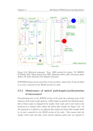
![Chapter 5 189 Optical TDMA-based switching fabrics
identical environmental influences in the tightly bound fibre bundle. Within the
READ section of a network node the marker clock comb is split again. The phase
of the reference clock comb and the marker clock combs are electrically received
and compared using a phase-locked loop (PLL.) The resulting error signal is used to
drive the variable optical delay/fibre stretcher (FS) which is configured to maintain
a constant differential phase between reference and marker signals by appropriate
adjustment of the fibre stretcher. Moreover since all N nodes implement this scheme
the optical path length from the headend to each node is maintained. Because
copies of the reference clock combs are directly derived from the common master
pulse source global synchronisation between the N nodes is assured. Consequently
timing wander or jitter within the TDMA frame is controlled. This ensures accurate
positioning of each data comb from the N nodes within their assigned TDMA slot
after the fan-out section of the N × N coupler.
5.7.5 Demultiplexing
The remaining copy of the marker clock comb within the READ section is used as
a gating signal to switch out the M-wavelength data modulated comb within the
timeslot of interest. A discrete, electrically addressable delay line is used to vary the
temporal coincidence of the gating signal with respect to the TDMA frame. This
allows different time slots to be chosen in an analogous manner to that used for Syn-
chroLAN. Chapter 4 referenced the work of Diez et al. [39] who have demonstrated
error-free demultiplexing of 8, 10Gbit/s data channels within one time slot from
an 8 slot frame—an aggregate bit rate of 640Gbit/s. In that work the AWG was
used to wavelength demultiplex the M wavelength channels into M separate fibres,
each terminated by a photodiode for the reception of data. In the present context
an AWG would be employed to the same effect, prior to a set of electoabsorption
modulators—one for each of the M separate fibres (or wavelength channels)—to
spatially separate the M wavelength data channels. Each separate wavelength is
then gated by an electroabsorption modulator to either impart data in the WRITE
section of a node or gate data within the READ section of a node.](https://image.slidesharecdn.com/a1b5bb05-a929-4e33-93de-a2dfe5b88eed-160311214335/85/thesis-208-320.jpg)
![Chapter 5 190 Optical TDMA-based switching fabrics
5.8 Constraints
5.8.1 Power distribution
The star has advantages over the linear, folded-bus topology of SynchroLAN. Firstly
the signal power distribution of the star is more uniform so the receivers require
less agility to cope with the dynamic power range. Recall that in Section 5.2.3
when describing the re-entrant bus topology the power ratio between channel 1 and
channel N, was given by [β(1−α)]
N−1
, which represented a quite considerable power
variation. Secondly the excess loss grows more slowly (logarithmically for the star
compared with linearly for the tapped bus.) To see this, a star whether, N × N or
1 × N, can be decomposed into an array of 2 × 2, 3dB couplers. Figure 5.14 shows
Input
16 outputs
(a)
(b)
16 inputs
3dB couplers
16 outputs
(c)
Figure 5.14: Composition of 16×16 and 1×16 couplers: a) 4×4 coupler; b) Several
4 × 4 couplers are suitably connected to form a 16 × 16 coupler; (c) 1 × 16 coupler.
this for both: (a) 16×16; (b) 1×16 and (c) 1×16. It follows that the internal path
traversed between an input port and an output port of an N × N coupler passes
through log2 N couplers. Each coupler has a tapping ratio of α = 1
2
(3dB) and an
excess loss, β. If the path of a single channel is traced (refer to Figure 5.15) then it
is possible to write an expression for the loss through the system. There are three
separate component families that introduce a loss. Firstly the 1×N coupler and the](https://image.slidesharecdn.com/a1b5bb05-a929-4e33-93de-a2dfe5b88eed-160311214335/85/thesis-209-320.jpg)
![Chapter 5 191 Optical TDMA-based switching fabrics
N × N coupler each have a loss of (0.5β)log2 N
. Each of the three separate AWGs in
the system have an insertion loss of ΓAWG. Finally there are two EAMs—one in the
WRITE section, one in the READ section—with associated lumped losses due to
splices given by γ. The output power of a single channel, P(i, j), where i represents
the time slot and j represents the wavelength by Equation 5.8
P(i, j) =
β
2
2 log2 N
× Γ3
AWG ×
1
2
γ2
× Pclk(j) (5.8)
We can determine the loss approximately by assuming the combined loss of the 1×N
and the N ×N coupler is 24dB (12dB + 12dB.) Each AWG will be assumed to have
an insertion loss of 5dB which gives a total of 15dB loss for the three elements in
the system. Finally the insertion loss of the EAM with the various lumped losses is
10dB at the WRITE section and 10dB at the READ section. The aggregated loss
is therefore ≈ 60dB. Therefore periodic optical amplification is required. However
there are constraints on the length of optical fibre deployed in the system and these
will be otlined in the next section.
5.8.2 Timing jitter and wavelength-dependent temporal skew
An obvious problem will arise from the difference due to temperature variations in
the surrounding environment acting on the optical fibre ‘spokes.’ that radiate from
the N × N coupler. This would be expected to advance/retard the clock pulse from
its assigned position leading to jitter-induced synchronisation errors. A very useful
study presented by Kato et al. [8] investigated the temperature dependence of the
chromatic dispersion for various fibre types. This dependence is formally represented
by Equation 5.9
dD
dθ
≈ S
dλ
dθ λ=λo
(5.9)
where D, is the group delay dispersion (defined earlier in Equation 2.25); λo, is the
zero-dispersion wavelength; θ, is the temperature; and S, is the dispersion slope.
The thermal coefficient term, dλ/dθ|λ=λo , provides the measure of interest. Sec-
tion 3.2.2.2 of Chapter 3 specified that for the 40Gbit/s SynchroLAN system the
timing jitter was required to be below 1ps. At 100Gbit/s this reduces to 400fs. Ex-
perimental measurements of the thermal coefficient for different fibre types is shown
in Table 5.2 [8]. We are now in a position to estimate the bound on the fibre length
subject to the likely operating conditions: themal excursion 100◦
C, ∆λ = 30nm
(the EDFA gain bandwidth.) If we take dλ/dθ|λ=λo ∼ 0.004 [(ps/nm/km)/◦
C] then](https://image.slidesharecdn.com/a1b5bb05-a929-4e33-93de-a2dfe5b88eed-160311214335/85/thesis-210-320.jpg)
![Chapter 5 192 Optical TDMA-based switching fabrics
Fibre type D S dλ/dθ|λ=λo
[(ps/nm/km)] [(ps/nm2
)/km] [(ps/nm/km)/◦
C]
NZ-DCF −2.2 +0.090 −0.0025
LCF −2.2 +0.121 +0.0038
DFF +3.6 +0.026 −0.0005
DCF2 −50.8 −0.154 −0.0040
Table 5.2: Optical fibre characteristics from ref. [8]. D, is the group delay dispersion;
λo, is the zero-dispersion wavelength; θ, is the temperature; So, is the dispersion
slope. dλ/dθ|λ=λo , is the thermal coefficient term. NZ-DSF: non-zero dispersion
shifted fibre, LCF: large-core fibre, DFF: dispersion-flattened fibre.
this translates into a delay of 12fs across a wavelength range of 30nm for a thermal
excursion of 100◦
C per metre of fibre. If we limit the span per ‘fibre spoke’ to ∼ 5m
(total optical path length is 20m!) length then this is within the specification.
It is still required to control the effect of mechanical strain or shock acting on
the optical fibre. This is where the two clock pulses come in. Briefly the error signal
from the differential path delays from the two clocks is used to drive the actuator
of an optical delay line based on a DVD-optical pick-up head [40]. This acts as a
tracking servo system to maintain the optical path length of each optical fibre arm
to maintain synchronisation.
The next problem is walk-off between the extremes of the wavelength range. The
dispersion function [41] is given by Equation 5.10
D(λ) =
Soλ
4
1 −
λo
λ
4
(5.10)
The maximum bit skew, ∆t, is defined by Equation 5.11 [42]
∆t = L
λf
λs
D(λ)dλ (5.11)
where L, is the length of the fibre sample, λf, is the wavelegnth of the fastest channel
and λs, is the wavelength of the slowest channel. This is equal to, Equation 5.12,
∆t =
LSoλ2
s
8
1 −
λf
λs
2
1 −
λo
λsλf
2
. (5.12)
if we define the wavelength interval as ∆λ and the centre wavelength of this interval
as, ¯λ then we can write λf = ¯λ + ∆λ/2 and λs = ¯λ − ∆λ/2. If these are substituted](https://image.slidesharecdn.com/a1b5bb05-a929-4e33-93de-a2dfe5b88eed-160311214335/85/thesis-211-320.jpg)
![Chapter 5 193 Optical TDMA-based switching fabrics
into Equation 5.12 then so long as ¯λ ∆λ then Equation 5.13 follows
∆t =
LSo ∆λ ¯λ
4
1 −
λo
¯λ
4
= L ∆λ D(¯λ). (5.13)
We are now in a position to estimate the skew for the interconnect. Assume, as
before, ∆λ = 30nm, L = 20m, and D(¯λ) = 17ps/nm/km—for standard fibre. The
skew, ∆t ≈ 10ps—one bit period! Obviously by choosing a fibre with a lower
dispersion it is possible to reduce the skew value, but the use of standard fibre is
deliberate not only because it is a common-off-the-shelf item, but also since the high
value of dispersion reduces non-linear effects such as stimulated raman scattering
(SRS) which would degrade the system. An approach that might work is to maintain
the high level of dispersion but alternate the dispersion slope such that data pulses
traveling towards the node would have one sign of dispersion slope, conversely data
pulses travelling from a node would have an equal but opposite sign. In this way
the walkoff between the wavelength extremes is compensated. However this would
be unwieldy in practice since it is necessary to ensure that all ‘spokes’ that radiate
from the hub are of equivalent length. The most useful technique is to include
appropriate optical and electrical delays so that the set of wavelength channels
within the assigned time slot at the ootput of the N × N coupler are temporally
coincident. Figure 5.15 graphically summarises this approach.
5.8.3 Interchannel Crosstalk
The finite rejection of the wavelength channels adjacent to the channel of interest at
each output port of the AWG demultiplexer leads to interchannel crosstalk which
degrades the fidelity of the received signal and increases the power penalty. This
undesirable effect depends on the number, M, of wavelength channels and is dis-
tinct from the intrachannel crosstalk between time channels that was described in
Section 3.2.2 of Chapter 3 in the context of a single wavelength channel OTDMA
system. Using the approach outlined in [43] it is possible to estimate the collective
impact of the finite rejection of each adjacent channel, i, on the system penalty
for both unamplified and amplified systems. (We will assume equal crosstalk per
channel.) For an unamplified system where the main contribution is from thermal
noise at the receiver the power penalty, δ, is given by Equation 5.14
δ = −10 log 1 −
M−1
i=1
i . (5.14)](https://image.slidesharecdn.com/a1b5bb05-a929-4e33-93de-a2dfe5b88eed-160311214335/85/thesis-212-320.jpg)
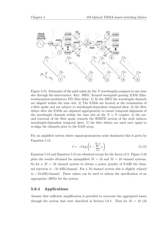

![Chapter 5 196 Optical TDMA-based switching fabrics
and data in orthogonal polarisation states along the span of the bus. An inte-
grated Mach-Zehnder Interferometer (IMZI) within the Read section of one node
allowed all-optical channel selection. This was the first demonstration of an all-
optical switching device within a local area network. The second demonstrator used
two conventional fibres, single-mode optical fibres within a blown fibre cable to
allow a dispersed switching fabric to be established across 300m of installed blown-
fibre [46] within a buildings infrastructure. This was possible because of the low
time-varying skew and timing jitter between optical pulses in the separate optical
fibres within the tightly-bound sheath. Channel selection was achieved exclusively
with electroabsorption modulators. The particular electroabsorption modulators
combined low polarisation sensitivity (<1dB) with high modulation depths (>30
dB) [45]. The electrical drive signals were either the two-tone technique [21], the
single impulse generator technique described in Chapter 4 [22] or a novel dual im-
pulse generator technique. The latter scheme used two impulse generators to gate
the EAM and it was compared with both the dual-fibre technique and the single
impulse generator method. The final part of the chapter outlined an extension to
the techniques exposed in SynchroLAN to a more speculative terabit interconnect
based on a star topology that included additional wavelength channels within each
time slot to increase the aggregated throughput of the system.](https://image.slidesharecdn.com/a1b5bb05-a929-4e33-93de-a2dfe5b88eed-160311214335/85/thesis-215-320.jpg)
![Bibliography
[1] N. J. Boden, D. Cohen, R. E. Feldermann, A. E. Kulawik, C. L. Seitz, J. N.
Seizovic, and W.-K. Su, “Myrinet: A gigabit-per-second local area network,”
IEEE Network, vol. 15, no. 1, pp. 29–36, February 1995.
[2] A. P. Perrier and P. R. Prucnal, “High-dimensionality shared-medium photonic
switch,” IEEE Trans. Commun., vol. 41, pp. 224–236, January 1993.
[3] J. K. Lucek, P. Gunning, D. G. Moodie, K. Smith, A. D. Ellis, and D. Pitcher,
“40 Gbit/s optical TDMA LAN,” Proc. ECOC ’96, vol. ThC.3.5, pp. 5.45—
5.48, September 1996.
[4] J. K. Lucek, P. Gunning, D. G. Moodie, K. Smith, and D. Pitcher, “Syn-
chrolan: A 40Gbit/s optical-TDMA LAN,” Electron Lett., vol. 33, no. 10,
pp. 887–888, 1997.
[5] P. J. Chidgey and D. W. Smith, “Sampled optical time-division multiplexing
of asynchronous data,” Electron. Lett., vol. 23, pp. 1228–1229, November 1987.
[6] K. J. Hood, P. W. Walland, C. L. Nuttal, L. J. St. Ville, T. P. Young,
A. Oliphant, R. P. Marsden, J. T. Zubrzycki, G. Cannel, C. Bunney, J. P.
Laude, and M. J. Anson, “Optical distribution systems for television studio
applications,” IEEE J. Lightwave Technol., vol. 11, pp. 956–958, May/June
1993.
[7] R. Ramaswami and K. N. Sivarajan, “Components,” in Optical Networks A
Practical Perspective (J. Mann, ed.), Optics and photonics, ch. 3, pp. 83–175,
San Diego: Morgan Kaufmann, 1 ed., 1998.
[8] T. Kato, Y. Koyano, and M. Nishimura, “Temperature dependence of chromatic
dispersion in various types of optical fiber,” Opt. Lett., vol. 25, no. 16, pp. 1156–
1159, August 2000.
197](https://image.slidesharecdn.com/a1b5bb05-a929-4e33-93de-a2dfe5b88eed-160311214335/85/thesis-216-320.jpg)
![Chapter 5 198 BIBLIOGRAPHY
[9] N. McKeown, “A fast switched backplane for a gigabit switched router,” Busi-
ness Comm. Review, vol. 27, no. 12, December 1997.
[10] N. McKeown, “The iSLIP scheduling algorithmn for input-queued switches,”
IEEE/ACM Trans. Networking, vol. 7, no. 2, pp. 188–201, April 1999.
[11] M. Shreedhar, “Efficient fair-queuing using defecit round-robin,” IEEE/ACM
Trans. Networking, vol. 4, no. 3, pp. 375–385, June 1996.
[12] I. Kaminow, “Photonic local networks,” in Optical Fiber Telecommunications
II (S. E. Miller and I. P. Kaminow, eds.), ch. 26, pp. 933–974, San Diego:
Academic Press, 1988.
[13] D. E. Altman and H. F. Taylor, “An eight terminal fiber optics data bus using
tee couplers,” Fiber Integ. Opt., vol. 1, no. 2, pp. 135–152, 1977.
[14] F. Auracher and H. H. Witte, “Optimized layout for a data bus system based
on a new planar access coupler,” Appl. Opt., vol. 16, no. 12, pp. 3140–3142,
December 1977.
[15] W. T. Cathey and B. J. Smith, “High concurrency data bus using arrays of
optical emitters and detectors,” Appl. Opt., vol. 18, no. 10, pp. 1687–1691,
15th May 1979.
[16] C. A. Villarruel, R. P. Moeller, and W. K. Burns, “Tapped tee single-mode data
distribution system,” IEEE J. Quantum Electron., vol. 17, no. 6, pp. 941–945,
June 1981.
[17] C. A. Villarruel, C. Wang, R. P. Moeller, and W. K. Burns, “Single-mode data
buses for local area network applications,” IEEE J. Lightwave Technol., vol. 3,
no. 3, pp. 472–478, June 1985.
[18] R. Ramaswami and K. Liu, “Research report: Analysis of optical bus networks
using doped-fiber amplifiers,” IBM research Report, vol. RC 18491, no. 80863,
pp. 1–29, May 1992.
[19] R. Hernandez-Lorenzo, P. Urquhart, J. K. Lucek, and P. Gunning., “High-
speed TDMA folded fibre bus LAN: design method,” Opt. Comm., vol. 142,
no. 1, pp. 26–29, October 1997.](https://image.slidesharecdn.com/a1b5bb05-a929-4e33-93de-a2dfe5b88eed-160311214335/85/thesis-217-320.jpg)
![Chapter 5 199 BIBLIOGRAPHY
[20] P. Gunning, J. K. Lucek, D. G. Moodie, K. Smith, R. P. Davey, S. V.
Chernikov, M. J. Guy, J. R. Taylor, and A. S. Siddiqui, “Gain-switched DFB
laser diode pulse source using continuous wave light injection for jitter suppres-
sion and an electroabsorption modulator for pedestal suppression,” Electron.
Lett., vol. 32, no. 11, pp. 1010–1011, 1996.
[21] J. K. Lucek, P. Gunning, D. G. Moodie, K. Smith, A. D. Ellis, and
D. Pitcher, “Optical-TDMA channel selection using electroabsorption modu-
lator with dual-frequency drive,” Electron Lett., vol. 33, no. 1, pp. 22–23, 1997.
[22] P. Gunning, J. K. Lucek, D. G. Moodie, K. Smith, D. Pitcher, and A. S. Sid-
diqui, “Fine-grain optical TDMA channel selection using an electroabsorption
modulator and impulse generator,” Electron. Lett., vol. 33, no. 2, pp. 146–157,
January 1997.
[23] P. R. Prucnal, M. F. Krol, and J. L. Stacy, “Demonstration of a rapidly tun-
able optical time-division multiple-access coder,” IEEE Photon. Technol. Lett.,
vol. 3, no. 2, pp. 170–172, February 1991.
[24] K.-L. Deng, K. I. Kang, I. Glask, and P. R. Prucnal, “A 1024-channel fast tun-
able delay line for ultrafast all-optical TDM networks,” IEEE Photon. Technol.
Lett., vol. 9, no. 11, pp. 1496–1498, November 1997.
[25] D. C. Rogers, J. V. Collins, C. W. Ford, P. Fiddyment, J. K. Lucek, M. Shabeer,
G. Sherlock, D. Cotter, K. Smith, J. D. Burton, C. M. Peed, A. E. Kelly, and
P. McKee, “Demonstration of programmable optical pulse pattern generator for
100Gbit/s networks,” Electron. Lett., vol. 31, pp. 2001–2002, November 1995.
[26] D. H. M. Spector, “Introduction,” in Building Linux Clusters, Sebastopol, CA:
O’Reilly & Associates, 1 ed., July 2000.
[27] C. Partridge, “Making hosts ready for gigabit networks,” in Gigabit Networking
(B. W. Kernighan, ed.), Addison-Wesley Professional Computing Series, ch. 9,
pp. 195–223, Reading, Massachusetts: Addison-Wesley, 1 ed., 1994.
[28] G. Brebner and R. Pooley, “ECOLE: A configurable environment for a lo-
cal optical network of workstations,” in Proc. 2nd International workshop on
communications and architecture support for network-based parallel computing
(CANPC ‘98), (G. Goos, J. Hartmanis, and J. van Leeuwen, eds.), vol. LNCS](https://image.slidesharecdn.com/a1b5bb05-a929-4e33-93de-a2dfe5b88eed-160311214335/85/thesis-218-320.jpg)
![Chapter 5 200 BIBLIOGRAPHY
1362 of Lecture Notes in Computer Science, pp. 45–58, Heidelberg: Springer-
Verlag, 1998. Las Vegas, Nevada, January 31 - February 1, 1998.
[29] G. Brebner, S. Cusack, T. Hopkins, and R. Pooley, “Interfacing networks of
workstations with the “fastest LAN in the world”: A work in progress re-
port,” February 1998. Computer Science Department, University of Edinburgh:
http://www.dcs.ed.ac.uk/ecole/HIdraft.ps.
[30] NSTC, “Large scale networking,” in FY1999 Blue Book: Computing, Informa-
tion, and Communications: Networked Computing for the 21st Century (August
1998) (S. E. Howe, ed.), ch. 7, pp. 41–60, Arlington, VA: National Science &
Technology Council, 1 ed., 1998. howe@ccic.gov.
[31] M. Zirngibl, C. H. Joyner, C. R. Doerr, L. W. Stultz, and H. M. Presby, “An
18-channel multifrequency laser,” IEEE Photon. Technol. Lett., vol. 8, no. 7,
pp. 870–872, July 1996.
[32] R. Monnard, A. K. Srivavesta, C. R. Doerr, C. H. Joyner, L. W. Stultz, M. Zirn-
gibl, Y. Sun, J. W. Sulhoff, J. L. Zyskind, and C. Wolf, “16-channel 50GHz
channel spacing long-haul transmitter for DWDM systems,” Electron. Lett.,
vol. 34, no. 8, pp. 765–767, April 1998.
[33] M. Zirngibl, “Multifrequency lasers and applications in WDM networks,” IEEE
Commun., vol. 36, no. 12, pp. 39–41, December 1998.
[34] P. C. Reeves-Hall, S. A. E. Lewis, D. G. Moodie, S. V. Chernikov, and J. R.
Taylor, “Simultaneous modulation of several WDM channels using a single
electro-absorption modulators,” Opt. Comm., vol. 175, no. 4–6, pp. 361–363,
March 2000.
[35] D. D. Marcenac, A. D. Ellis, and D. G. Moodie, “80Gbit/s OTDM using elec-
troabsorption modulators,” Electron. Lett., vol. 34, no. 1, pp. 101–103, January
1998.
[36] M. J. Guy, S. V. Chernikov, and J. R. Taylor, “A duration tunable, multi-
wavelength pulse source for OTDM and WDM communication systems,” IEEE
Photon. Technol. Lett., vol. 9, no. 7, pp. 1017–1019, July 1997.
[37] S. M. Ojha, C. Cureton, T. Bricheno, S. Day, D. Moule, A. J. Bell, and J. Taylor,
“Simple method of fabricating polarisation-insensitive and very low crosstalk
AWG grating devices,” Electron. Lett., vol. 34, no. 1, pp. 78–79, January 1998.](https://image.slidesharecdn.com/a1b5bb05-a929-4e33-93de-a2dfe5b88eed-160311214335/85/thesis-219-320.jpg)
![Chapter 5 201 BIBLIOGRAPHY
[38] K. A. McGreer, “Arrayed waveguide gratings for wavelength routing,” IEEE
Commun., vol. 36, no. 12, pp. 62–68, December 1998.
[39] S. Diez, R. Ludwig, and H. G. Weber, “All-optical switch for TDM and
WDM/TDM systems demonstrated in a 640Gbit/s demultiplexing experi-
ment,” Electron. Lett., vol. 34, no. 8, pp. 803–805, April 1998.
[40] M. Shinoda, K. Nakamura, M. Yabe, N. Watanabe, T. Satoh, N. Hirai, N. Fu-
jita, K. Kime, and Y. Ishida, “Optical pick-up DVD,” IEEE Trans. Consumer
Electronics, vol. 42, no. 3, pp. 808–813, August 1996.
[41] British Telecommunications, “Specification CW1505H for step-index single-
mode optical fibres,” June 1996.
[42] G. Jeong and J. W. Goodman, “Long-distance parallel data link using
WDM transmission with bit-skew compensation,” IEEE J. Lightwave Technol.,
vol. LT-14, no. 5, pp. 655–660, May 1996.
[43] R. Ramaswami and K. N. Sivarajan, “Modulation and demodulation,” in Op-
tical Networks A Practical Perspective (J. Mann, ed.), Optics and photonics,
ch. 5, pp. 203–261, San Diego: Morgan Kaufmann, 1 ed., 1998.
[44] D. Cotter, J. K. Lucek, and D. D. Marcenac, “Ultra-high bit-rate networking:
From the transcontinental backbone to the desktop,” IEEE Commun. Mag.,
vol. 35, pp. 90–95, April 1997.
[45] D. G. Moodie, P. J. Cannard, A. J. Dann, D. D. Marcenac, C. W. Ford,
J. Reed, R. T. Moore, J. K. Lucek, and A. D. Ellis, “Low polarisation sen-
sitivity electroabsorption modulators for 160 Gbit/s network,” Electron. Lett.,
vol. 33, no. 24, pp. 2068–2070, November 1997.
[46] K. W. Cobb, P. D. Jenkins, I. MacKenzie, and D. J. Stockton, “Fibre campus
networks,” BT Telecom. Eng., vol. 11, no. 3, pp. 112–117, 1992.
[47] R. Hernandez-Lorenzo, P. Urquhart, and M. Lopez-Amo, “Folded fibre bus
interconnects with distributed amplification,” Opt. Comm., vol. 152, no. 1–3,
pp. 31–35, June 1998.
[48] A. Altuncu, L. N¨oel, W. A. Pender, A. S. Siddiqui, T. Widdowson, A. D. Ellis,
M. A. Newhouse, A. J. Antos, G. Kar, and P. W. Chu, “40 Gbit/s error free](https://image.slidesharecdn.com/a1b5bb05-a929-4e33-93de-a2dfe5b88eed-160311214335/85/thesis-220-320.jpg)
![Chapter 5 202 BIBLIOGRAPHY
transmission over a 68km distributed erbium doped fibre amplifier,” Electron.
Lett., vol. 32, no. 3, pp. 233–234, February 1996.
[49] J. K. Lucek and K. Smith, “All-optical signal regenerator,” Opt. Lett., vol. 18,
no. 10, pp. 1226–1228, 1993.
[50] W. A. Pender, T. Widdowson, and A. D. Ellis, “Error free operation of a 40
Gbit/s all-optical regenerator,” Electron. Lett., vol. 32, no. 6, pp. 567–569,
March 1996.
[51] J. R. Heath, P. J. Kuekes, G. S. Snider, and R. S. Williams, “A defect-tolerant
computer architecture: opportunities for nanotechnology,” Science, vol. 280,
no. 5370, pp. 1716–1721, June 1998.
[52] D. Psaltis, “Holographic data storage,” IEEE Computer, vol. 31, no. 2, pp. 52–
60, February 1998.
[53] J. K. Lucek, A. D. Ellis, D. G. Moodie, D. Pitcher, P. Gunning, and D. Cot-
ter, “100Gbit/s parallel-to-serial and serial-to-parallel conversion using elec-
troabsorption modulators,” IEEE/LEOS Summer topical meeting: Broadband
Optical Networks and Technologies, vol. 1, pp. 25–26, July 1998.](https://image.slidesharecdn.com/a1b5bb05-a929-4e33-93de-a2dfe5b88eed-160311214335/85/thesis-221-320.jpg)


![Chapter 6 207 Conclusions
isolation and component-reliability are areas that are worthy of additional study.
Many algorithmns are now available for conventional electronic switching fabrics
which rely on some degree of parallelism at the metallic track level to overcome
the bandwidth limitations. Might they be usefully ported to the optical switching
fabrics that have been reported in this thesis? No mention was made as to how
multiple switching fabrics might in-turn be interconnected. Certainly with optical
regeneration the modular nature of the fabric could form larger, richer interconnects.
Given the emphasis on synchronisation how might this be assured across a collection
of switching fabrics? One answer might be that of asynchronous digital optical
regeneration [1, 2] which can accomodate the synchronisation issues across a network
of switching fabrics. This would prove a particularly fruitful area of research. Finally,
the interconnects that were presented may provide an upgrade path between present-
day electronic switch-based packet networks, typified by routers in particular, and
the holy-grail of photonic packet routing. This thesis, I hope, provided a stepping-
stone along this path.](https://image.slidesharecdn.com/a1b5bb05-a929-4e33-93de-a2dfe5b88eed-160311214335/85/thesis-226-320.jpg)
![Bibliography
[1] D. Cotter and A. D. Ellis, “Asynchronous digital optical regeneration and net-
works,” IEEE J. Lightwave Technol.., vol. 16, pp. 2068–2080, December 1998.
[2] P. Gunning, I. D. Phillips, A. D. Ellis, J. K. Lucek, D. G. Moodie, and D. Cot-
ter, “10Gbit/s asynchronous digital optical regenerator,” Proc. OFC/IOOC
1999, vol. 1, pp. 134–136, February 1999.
208](https://image.slidesharecdn.com/a1b5bb05-a929-4e33-93de-a2dfe5b88eed-160311214335/85/thesis-227-320.jpg)

![Chapter A 210 Maxwells equations
It is most convenient to consider Equation A.7 in cylindrical co-ordinates
2
E = 2
Er −
2
r2
∂Eφ
∂φ
−
Er
r2
r
|r|
(A.9)
+ 2
Eφ +
2
r2
∂Er
∂φ
−
Eφ
r2
φ (A.10)
+ 2
Ez z (A.11)
= − µoµ o
∂2
Er
∂t2
r − µoµ o
∂2
Eφ
∂t2
φ − µoµ o
∂2
Ez
∂t2
z (A.12)
The scalar wave equation along the direction of propagation (z can be obtained from
Equation A.12 [1]
2
Ez = −µoµ o
∂2
Ez
∂t2
(A.13)
which is the scalar wave equation. The Laplacian ( 2
in cylindrical co-ordinates
which is the most appropriate for an optical fibre is represented as
∂2
Ez
∂r2
+
1
r
∂Ez
∂r
+
1
r2
∂2
Ez
∂φ2
+
∂2
Ez
∂z2
= −µoµ o
∂2
Ez
∂t2
(A.14)
The separation of variables technique can be used to obtain solutions of Equa-
tion A.14
Ez(r, φ, z, t) = R(r)Φ(φ)Z(z)T(t) ≡ RΦZT (A.15)
Substituting this into Equation A.14 and dividing across by Equation A.15 gives the
1-d equation
1
R
d2
R
dr2
+
1
r
1
R
dR
dr
+
1
r2
1
Φ
d2
Φ
dφ2
+
1
Z
d2
Z
dz2
= −µoµ o
1
T
d2
T
dt2
(A.16)
These can then be solved by conventional techniques to provide a full description of
the field solutions within the optical fibre.](https://image.slidesharecdn.com/a1b5bb05-a929-4e33-93de-a2dfe5b88eed-160311214335/85/thesis-229-320.jpg)
![Bibliography
[1] W. Van Etten and J. van der Platts, Fundamentals of Optical Fiber Communi-
cations. International Series in Optoelectronics, London: Prentice-Hall, 1 ed.,
1991.
211](https://image.slidesharecdn.com/a1b5bb05-a929-4e33-93de-a2dfe5b88eed-160311214335/85/thesis-230-320.jpg)
![Appendix A
Publications
The work described in this thesis has been the subject of a patent, a patent appli-
cation, as well as journal and conference papers. It has contributed to two book
chapters and has been referenced within two graduate textbooks in photonics. The
following sections list this output.
A.1 Patents
A US Patent [1] (reproduced in Appendix B, Page 219) was awarded based on the
hybrid pulse source described in Section 3.6. A patent application [2] has been
drafted based on the work sketched in Section 5.7.
A.2 Journal and Conference papers
Paper [3] (reproduced in Appendix B, Page 231) was based on the work described in
Section 3.3.3. Papers [4, 5, 6] describes work that used the gain-switched DFB pulse
source and non-linear compression techniques described in Section 3.3.4. Paper [7]
did not explicitly use any of the work reported in this thesis—my contribution
was to use my expertise in the area of gain-switched DFBs, linear and nonlinear
pulse compression to assist the principal author. Paper [8] used the gain-switched
DFB pulse source and non-linear compression techniques described in Section 3.3.4.
Papers [9, 10] did not explicitly use any of the work reported in this thesis—my
contribution was as to use my expertise in the area of gain-switched DFBs, linear
and nonlinear pulse compression to assist the principal author. Paper [11] was based
on the hybrid pulse source described in Section 3.6. Paper [12] describes work that
212](https://image.slidesharecdn.com/a1b5bb05-a929-4e33-93de-a2dfe5b88eed-160311214335/85/thesis-231-320.jpg)
![Chapter A 213 Publications
used the gain-switched DFB pulse source and non-linear compression techniques de-
scribed in Section 3.3.4. Paper [13] (reproduced in Appendix B, Page 233) was based
on the hybrid pulse source described in Section 3.6. Paper [14] describes work that
used the gain-switched DFB pulse source and non-linear compression techniques
described in Section 3.3.4. Paper [15] used the hybrid pulse source described in Sec-
tion 3.6 both in terms of the pulse source that was used to provide the RZ optical
pulses but also in terms of the dual-frequency EA modulator demultiplexing used
for each node. Paper [16] described work that used the gain-switched DFB pulse
source and non-linear compression techniques described in Section 3.3.4. Paper [17]
described work that used the gain-switched DFB pulse source and non-linear com-
pression techniques described in Section 3.3.4. Paper [18] used the hybrid pulse
source described in Section 3.6 both in terms of the pulse source that was used to
provide the RZ optical pulses but also in terms of the dual-frequency EA modu-
lator demultiplexing used for each node. Paper [19] (reproduced in Appendix B,
Page 235) used the hybrid pulse source described in Section 3.6 both in terms of the
pulse source that was used to provide the RZ optical pulses but also in terms of the
dual-frequency EA modulator demultiplexing used for each node. In addition the
use of 2.5 GHz impulse generators were used for de-multiplexing which was described
in Section 4.2. Paper [20] was a review paper that described work that used the
gain-switched DFB pulse source and non-linear compression techniques described in
Section 3.3.4. It also contained additional work that was not described in this thesis
in the area of gain-switched DFBs. Paper [21] used the hybrid pulse source described
in Section 3.6 both in terms of the pulse source that was used to provide the RZ
optical pulses but also in terms of the dual-frequency EA modulator demultiplexing
used for each node. Paper [22] used the hybrid pulse source described in Section 3.6
both in terms of the pulse source that was used to provide the RZ optical pulses
but also in terms of the dual-frequency EA modulator demultiplexing used for each
node. Paper [23] (reproduced in Appendix B, Page 237) was based on the work on
non-linear deultiplexing described in Section 4.3 as well as the optical interconnect
described in Section 5.3. Paper [24] describes work that used the gain-switched
DFB pulse source and non-linear compression techniques described in Section 3.3.4.
Paper [25] was based on the optical interconnect work described in Section 5.4. Pa-
per [26] which was utilised in Section 5.2.5 used real measurements based on the
SynchroLAN interconnect. Paper [27] (reproduced in Appendix B, Page 239) was
based on the optical interconnect work described in Section 5.4. Paper [28] was not
explicitly reported in this thesis. However expertise in the area of EA modulator](https://image.slidesharecdn.com/a1b5bb05-a929-4e33-93de-a2dfe5b88eed-160311214335/85/thesis-232-320.jpg)
![Chapter A 214 Publications
demultiplexing was used that was built-up during the course of the thesis was used.
A.3 Book Chapters
Both book chapters [29, 30] described work that used the gain-switched DFB pulse
source and non-linear compression techniques described in Section 3.3.4.
A.4 Textbook references
The graduate textbook [31] referenced the work that is reproduced in Appendix B,
Page 231 that was based on the work reported in Section 3.3.3. The graduate
textbook [32] explicitly referenced the work described in [23] (reproduced in Ap-
pendix B, Page 237) that was based on the work on non-linear deultiplexing de-
scribed in Section 4.3 as well as the optical interconnect described in Section 5.3.
The book also explicitly referenced the work described in [27] (reproduced in Ap-
pendix B, Page 239) which was based on the optical interconnect work described in
Section 5.4.](https://image.slidesharecdn.com/a1b5bb05-a929-4e33-93de-a2dfe5b88eed-160311214335/85/thesis-233-320.jpg)
![Bibliography
[1] P. Gunning, R. Davey, D. G. Moodie, K. Smith, J. Lucek, and D. Nesset,
“Optical pulse source,” US Patent, no. 5,778,015, Filed May 16, 1996; Assigned
July 7, 1998.
[2] P. Gunning, “Photonic switching fabric,” US Patent, in preparation.
[3] P. Gunning, R. Kashyap, A. S. Siddiqui, and K. Smith, “Picosecond pulse
generation of <5ps from a gain-switched DFB semiconductor laser diode using
a linearly step-chirped fibre grating,” Electron. Lett., vol. 31, no. 13, pp. 1066–
1067, 1995.
[4] D. Cotter, J. K. Lucek, M. Shabeer, K. Smith, P. Gunning, and D. C. Rogers,
“Ultrafast self-routing packet networks (invited paper),” EFOC&N’95, June
1995.
[5] D. Cotter, J. K. Lucek, M. Shabeer, K. Smith, D. C. Rogers, P. Gunning,
and D. Nesset, “100Gbit/s packet self-routing using all-optical 6-bit ‘keyword’
address recognition,” Proc. ECOC ’95, vol. 2, pp. 637–640, September 1995.
[6] D. Cotter, J. K. Lucek, M. Shabeer, D. C. Rogers, D. Nesset, and P. Gunning,
“Self-routing of 100Gbit/s packets using 6-bit ‘keyword’ address recognition,”
Electron. Lett., vol. 31, no. 25, pp. 2201–2202, December 1995.
[7] R. P. Davey, K. Smith, R. Wyatt, D. L. Williams, M. J. Holmes, D. M. Pataca,
M. L. Rocha, and P. Gunning, “Subpicosecond pulse generation from a 1.3µm
DFB laser gain-switched at 1GHz,” Electron. Lett., vol. 32, no. 4, pp. 349–351,
February 1996.
[8] D. C. Rogers, J. V. Collins, C. W. Ford, J. K. Lucek, M. Shabeer, G. Sherlock,
D. Cotter, K. Smith, C. M. Peed, A. E. Kelly, P. Gunning, D. Nesset, and I. F.
Lealman, “Demonstration of programmable optical pulse pattern generator for
100Gbit/s networks,” Proc. OFC’96, February 1996.
215](https://image.slidesharecdn.com/a1b5bb05-a929-4e33-93de-a2dfe5b88eed-160311214335/85/thesis-234-320.jpg)
![Chapter A 216 BIBLIOGRAPHY
[9] D. M. Pataca, M. L. Rocha, R. P. Davey, K. Smith, R. Wyatt, and P. Gunning,
“Transmission of 5 ps solitons at 1.32µm over 50 km of standard fibre using
praseodymium doped fluoride fibre amplifiers,” Electron. Lett., vol. 32, no. 8,
pp. 754–755, April 1996.
[10] R. P. Davey, K. Smith, D. L. Williams, R. Kashyap, M. J. Holmes, D. M. Pat-
aca, M. L. Rocha, and P. Gunning, “Ultrashort pulse generation and process-
ing at 1.3µm for ultra-high speed photonic networks,” IEE Colloquium “High
Speed and Long Distance Optical Transmission”, April 1996.
[11] P. Gunning, J. K. Lucek, D. G. Moodie, K. Smith, R. P. Davey, S. V.
Chernikov, M. J. Guy, and A. S. Siddiqui, “CW injected, low-jitter, low-
pedestal, gain-switched DFB-SLD/electroabsorption modulator-based pulse
source at 1.5µm for ultrafast network applications,” IEE Colloquium “High
Speed and Long Distance Optical Transmission”, April 1996.
[12] D. Cotter, M. C. Tatham, J. K. Lucek, M. Shabeer, K. Smith, D. C. Rogers,
D. Nesset, and P. Gunning, “Photonic address-header recognition and self-
routing in ultrafast packet networks,” IEEE/OSA 1996 International Topical
Meeting on Photonics in Switching, 21–25 April 1996.
[13] P. Gunning, J. K. Lucek, D. G. Moodie, K. Smith, R. P. Davey, S. V.
Chernikov, M. J. Guy, J. R. Taylor, and A. S. Siddiqui, “Gain-switched DFB
laser diode pulse source using continuous wave light injection for jitter suppres-
sion and an electroabsorption modulator for pedestal suppression,” Electron.
Lett., vol. 32, no. 11, pp. 1010–1011, May 1996.
[14] D. Cotter, M. C. Tatham, J. K. Lucek, M. Shabeer, K. Smith, D. Nesset, D. C.
Rogers, and P. Gunning, “Ultrafast all-optical signal processing for packet
switching,” Proc. 1996 International workshop on photonic network technolo-
gies, September 1996.
[15] J. K. Lucek, P. Gunning, D. G. Moodie, K. Smith, A. D. Ellis, and D. Pitcher,
“40 Gbit/s optical TDMA LAN,” Proc. ECOC ’96, vol. ThC.3.5, pp. 5.45—
5.48, September 1996.
[16] D. Cotter, J. K. Lucek, K. Smith, P. Gunning, and R. P. Davey, “Ultrafast
photonic networking (invited),” IEEE LEOS’96, November 1996.](https://image.slidesharecdn.com/a1b5bb05-a929-4e33-93de-a2dfe5b88eed-160311214335/85/thesis-235-320.jpg)
![Chapter A 217 BIBLIOGRAPHY
[17] J. K. Lucek, D. Cotter, K. Smith, and P. Gunning, “Ultrafast photonic data
networks,” IEEE LEOS’96, vol. 2, pp. 86–87, November 1996.
[18] J. K. Lucek, P. Gunning, D. G. Moodie, K. Smith, A. D. Ellis, and
D. Pitcher, “Optical-TDMA channel selection using electroabsorption modula-
tor with dual-frequency drive,” Electron Lett., vol. 33, no. 1, pp. 22–23, January
1997.
[19] P. Gunning, J. K. Lucek, D. G. Moodie, K. Smith, D. Pitcher, and A. S. Sid-
diqui, “Fine-grain optical TDMA channel selection using an electroabsorption
modulator and impulse generator,” Electron. Lett., vol. 33, no. 2, pp. 146–148,
January 1997.
[20] D. M. Pataca, P. Gunning, M. L. Rocha, J. K. Lucek, R. Kashyap, K. Smith,
R. P. Davey, D. G. Moodie, K. Smith, R. F. Souza, and A. S. Siddiqui, “Gain-
switched DFB lasers,” Brazil. J. Microwaves and Optoelectron., vol. 1, no. 1,
pp. 46–63, May 1997.
[21] J. K. Lucek, P. Gunning, D. G. Moodie, K. Smith, and D. Pitcher, “Syn-
chrolan: A 40Gbit/s optical-TDMA LAN,” Electron Lett., vol. 33, no. 10,
pp. 887–888, May 1997.
[22] P. Gunning, J. K. Lucek, D. G. Moodie, K. Smith, and D. Pitcher, “Demon-
stration of 40 Gbit/s interconnect using optical time division multiple access,”
Proc. 8th Annual Workshop on Interconnects within High-Speed Digital Sys-
tems, May 1997.
[23] P. Gunning, J. K. Lucek, D. Nesset, J. V. Collins, C. W. Ford, D. Pitcher,
K. Smith, D. Cotter, E. Jahn, N. Agrawal, and A. S. Siddiqui, “Optical-TDMA
LAN incorporating packaged integrated Mach-Zehnder interferometer channel
selector,” Electron. Lett., vol. 33, no. 16, pp. 1404–1406, 1997.
[24] D. Cotter, J. Lucek, P. Gunning, A. J. Poustie, K. J. Blow, and R. J. Manning,
“Ultrafast photonic self-routing,” IOOC-ECOC97, vol. 2, pp. 67–68, September
1997.
[25] P. Gunning, J. K. Lucek, D. G. Moodie, K. Smith, D. Pitcher, Q. Badat, and
A. S. Siddiqui, “40 Gbit/s optical-TDMA LAN over 300 metres installed blown
fibre,” IOOC-ECOC97, vol. 4, pp. 61–64, September 1997.](https://image.slidesharecdn.com/a1b5bb05-a929-4e33-93de-a2dfe5b88eed-160311214335/85/thesis-236-320.jpg)
![Chapter A 218 BIBLIOGRAPHY
[26] R. Hernandez-Lorenzo, P. Urquhart, J. K. Lucek, and P. Gunning., “High-
speed TDMA folded fibre bus LAN: design method,” Opt. Comm., vol. 142,
no. 1, pp. 26–29, October 1997.
[27] P. Gunning, J. K. Lucek, D. G. Moodie, K. Smith, D. Pitcher, Q. Badat, and
A. S. Siddiqui, “SynchroLan: 40 Gbit/s optical-TDMA LAN using installed
blown-fibre,” Electron. Lett., vol. 34, no. 5, pp. 488–490, March 1998.
[28] J. K. Lucek, A. D. Ellis, D. G. Moodie, D. Pitcher, P. Gunning, and D. Cot-
ter, “100Gbit/s parallel-to-serial and serial-to-parallel conversion using elec-
troabsorption modulators,” IEEE/LEOS Summer topical meeting: Broadband
Optical Networks and Technologies, vol. 1, pp. 25–26, July 1998.
[29] D. Cotter, M. C. Tatham, J. K. Lucek, K. Smith, and P. Gunning, “Ultrafast
all-optical signal processing for packet switching,” in Photonic Networks: Ad-
vances in Communications (G. Prati, ed.), ch. 1, pp. 401–413, Berlin: Springer-
Verla, 1 ed., 1997.
[30] D. Cotter, J. K. Lucek, P. Gunning, D. G. Moodie, A. Poustie, K. J. Blow,
and R. J. Manning, “Ultrafast networks using high-speed RZ optical pulses
for transmission, routing and processing,” in New Trends in Optical Soliton
Communications (A. Hasegawa, ed.), Dordrecht: Klewer, 1 ed., 1998.
[31] R. Kashyap, “Fiber grating lasers and amplifiers,” in Fiber Bragg Gratings
(P. L. Kelly, I. Kaminow, and G. Agrawal, eds.), Optics and Photonics, ch. 8,
pp. 381–382, San Diego: Academic Press, 1 ed., 1999.
[32] R. Ramaswami and K. N. Sivarajan, “Photonic packet switching,” in Optical
Networks A Practical Perspective (J. Mann, ed.), The Morgan Kaufmann series
in Networking, ch. 14, p. 543, San Diego: Morgan Kaufmann, 1 ed., 1998.](https://image.slidesharecdn.com/a1b5bb05-a929-4e33-93de-a2dfe5b88eed-160311214335/85/thesis-237-320.jpg)