![Vol. 3A 10-17
ADVANCED PROGRAMMABLE INTERRUPT CONTROLLER (APIC)
The timer can be configured through the timer LVT entry for one-shot or periodic operation. In one-shot mode, the
timer is started by programming its initial-count register. The initial count value is then copied into the current-
count register and count-down begins. After the timer reaches zero, an timer interrupt is generated and the timer
remains at its 0 value until reprogrammed.
In periodic mode, the current-count register is automatically reloaded from the initial-count register when the
count reaches 0 and a timer interrupt is generated, and the count-down is repeated. If during the count-down
process the initial-count register is set, counting will restart, using the new initial-count value. The initial-count
register is a read-write register; the current-count register is read only.
A write of 0 to the initial-count register effectively stops the local APIC timer, in both one-shot and periodic mode.
The LVT timer register determines the vector number that is delivered to the processor with the timer interrupt that
is generated when the timer count reaches zero. The mask flag in the LVT timer register can be used to mask the
timer interrupt.
10.5.4.1 TSC-Deadline Mode
The mode of operation of the local-APIC timer is determined by the LVT Timer Register. Specifically:
• If CPUID.01H:ECX.TSC_Deadline[bit 24] = 0, the mode is determined by bit 17 of the register.
• If CPUID.01H:ECX.TSC_Deadline[bit 24] = 1, the mode is determined by bits 18:17. See Figure 10-8. (If
CPUID.01H:ECX.TSC_Deadline[bit 24] = 0, bit 18 of the register is reserved.)
A write to the LVT Timer Register that changes the timer mode disarms the local APIC timer. The supported timer
modes are given in Table 10-2. The three modes of the local APIC timer are mutually exclusive.
TSC-deadline mode allows software to use the local APIC timer to signal an interrupt at an absolute time. In TSC-
deadline mode, writes to the initial-count register are ignored; and current-count register always reads 0. Instead,
timer behavior is controlled using the IA32_TSC_DEADLINE MSR.
The IA32_TSC_DEADLINE MSR (MSR address 6E0H) is a per-logical processor MSR that specifies the time at which
a timer interrupt should occur. Writing a non-zero 64-bit value into IA32_TSC_DEADLINE arms the timer. An inter-
rupt is generated when the logical processor’s time-stamp counter equals or exceeds the target value in the
IA32_TSC_DEADLINE MSR.3 When the timer generates an interrupt, it disarms itself and clears the
IA32_TSC_DEADLINE MSR. Thus, each write to the IA32_TSC_DEADLINE MSR generates at most one timer inter-
rupt.
In TSC-deadline mode, writing 0 to the IA32_TSC_DEADLINE MSR disarms the local-APIC timer. Transitioning
between TSC-deadline mode and other timer modes also disarms the timer.
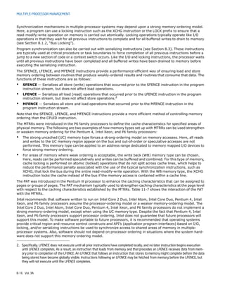
Figure 10-11. Initial Count and Current Count Registers
Table 10-2. Local APIC Timer Modes
LVT Bits [18:17] Timer Mode
00b One-shot mode, program count-down value in an initial-count register. See Section 10.5.4
01b Periodic mode, program interval value in an initial-count register. See Section 10.5.4
10b TSC-Deadline mode, program target value in IA32_TSC_DEADLINE MSR.
11b Reserved
31 0
Initial Count
Address: Initial Count
Value after reset: 0H
Current Count
Current Count FEE0 0390H
FEE0 0380H](data:image/gif;base64,R0lGODlhAQABAIAAAAAAAP///yH5BAEAAAAALAAAAAABAAEAAAIBRAA7)
Recommended
More Related Content
Similar to summary intel spec for "msr reg" memory order
Similar to summary intel spec for "msr reg" memory order (20)
Recently uploaded
Recently uploaded (20)
summary intel spec for "msr reg" memory order
- 1. 8-16 Vol. 3A MULTIPLE-PROCESSOR MANAGEMENT Synchronization mechanisms in multiple-processor systems may depend upon a strong memory-ordering model. Here, a program can use a locking instruction such as the XCHG instruction or the LOCK prefix to ensure that a read-modify-write operation on memory is carried out atomically. Locking operations typically operate like I/O operations in that they wait for all previous instructions to complete and for all buffered writes to drain to memory (see Section 8.1.2, “Bus Locking”). Program synchronization can also be carried out with serializing instructions (see Section 8.3). These instructions are typically used at critical procedure or task boundaries to force completion of all previous instructions before a jump to a new section of code or a context switch occurs. Like the I/O and locking instructions, the processor waits until all previous instructions have been completed and all buffered writes have been drained to memory before executing the serializing instruction. The SFENCE, LFENCE, and MFENCE instructions provide a performance-efficient way of ensuring load and store memory ordering between routines that produce weakly-ordered results and routines that consume that data. The functions of these instructions are as follows: • SFENCE — Serializes all store (write) operations that occurred prior to the SFENCE instruction in the program instruction stream, but does not affect load operations. • LFENCE — Serializes all load (read) operations that occurred prior to the LFENCE instruction in the program instruction stream, but does not affect store operations.2 • MFENCE — Serializes all store and load operations that occurred prior to the MFENCE instruction in the program instruction stream. Note that the SFENCE, LFENCE, and MFENCE instructions provide a more efficient method of controlling memory ordering than the CPUID instruction. The MTRRs were introduced in the P6 family processors to define the cache characteristics for specified areas of physical memory. The following are two examples of how memory types set up with MTRRs can be used strengthen or weaken memory ordering for the Pentium 4, Intel Xeon, and P6 family processors: • The strong uncached (UC) memory type forces a strong-ordering model on memory accesses. Here, all reads and writes to the UC memory region appear on the bus and out-of-order or speculative accesses are not performed. This memory type can be applied to an address range dedicated to memory mapped I/O devices to force strong memory ordering. • For areas of memory where weak ordering is acceptable, the write back (WB) memory type can be chosen. Here, reads can be performed speculatively and writes can be buffered and combined. For this type of memory, cache locking is performed on atomic (locked) operations that do not split across cache lines, which helps to reduce the performance penalty associated with the use of the typical synchronization instructions, such as XCHG, that lock the bus during the entire read-modify-write operation. With the WB memory type, the XCHG instruction locks the cache instead of the bus if the memory access is contained within a cache line. The PAT was introduced in the Pentium III processor to enhance the caching characteristics that can be assigned to pages or groups of pages. The PAT mechanism typically used to strengthen caching characteristics at the page level with respect to the caching characteristics established by the MTRRs. Table 11-7 shows the interaction of the PAT with the MTRRs. Intel recommends that software written to run on Intel Core 2 Duo, Intel Atom, Intel Core Duo, Pentium 4, Intel Xeon, and P6 family processors assume the processor-ordering model or a weaker memory-ordering model. The Intel Core 2 Duo, Intel Atom, Intel Core Duo, Pentium 4, Intel Xeon, and P6 family processors do not implement a strong memory-ordering model, except when using the UC memory type. Despite the fact that Pentium 4, Intel Xeon, and P6 family processors support processor ordering, Intel does not guarantee that future processors will support this model. To make software portable to future processors, it is recommended that operating systems provide critical region and resource control constructs and API’s (application program interfaces) based on I/O, locking, and/or serializing instructions be used to synchronize access to shared areas of memory in multiple- processor systems. Also, software should not depend on processor ordering in situations where the system hard- ware does not support this memory-ordering model. 2. Specifically, LFENCE does not execute until all prior instructions have completed locally, and no later instruction begins execution until LFENCE completes. As a result, an instruction that loads from memory and that precedes an LFENCE receives data from mem- ory prior to completion of the LFENCE. An LFENCE that follows an instruction that stores to memory might complete before the data being stored have become globally visible. Instructions following an LFENCE may be fetched from memory before the LFENCE, but they will not execute until the LFENCE completes.
- 2. Vol. 3A 10-17 ADVANCED PROGRAMMABLE INTERRUPT CONTROLLER (APIC) The timer can be configured through the timer LVT entry for one-shot or periodic operation. In one-shot mode, the timer is started by programming its initial-count register. The initial count value is then copied into the current- count register and count-down begins. After the timer reaches zero, an timer interrupt is generated and the timer remains at its 0 value until reprogrammed. In periodic mode, the current-count register is automatically reloaded from the initial-count register when the count reaches 0 and a timer interrupt is generated, and the count-down is repeated. If during the count-down process the initial-count register is set, counting will restart, using the new initial-count value. The initial-count register is a read-write register; the current-count register is read only. A write of 0 to the initial-count register effectively stops the local APIC timer, in both one-shot and periodic mode. The LVT timer register determines the vector number that is delivered to the processor with the timer interrupt that is generated when the timer count reaches zero. The mask flag in the LVT timer register can be used to mask the timer interrupt. 10.5.4.1 TSC-Deadline Mode The mode of operation of the local-APIC timer is determined by the LVT Timer Register. Specifically: • If CPUID.01H:ECX.TSC_Deadline[bit 24] = 0, the mode is determined by bit 17 of the register. • If CPUID.01H:ECX.TSC_Deadline[bit 24] = 1, the mode is determined by bits 18:17. See Figure 10-8. (If CPUID.01H:ECX.TSC_Deadline[bit 24] = 0, bit 18 of the register is reserved.) A write to the LVT Timer Register that changes the timer mode disarms the local APIC timer. The supported timer modes are given in Table 10-2. The three modes of the local APIC timer are mutually exclusive. TSC-deadline mode allows software to use the local APIC timer to signal an interrupt at an absolute time. In TSC- deadline mode, writes to the initial-count register are ignored; and current-count register always reads 0. Instead, timer behavior is controlled using the IA32_TSC_DEADLINE MSR. The IA32_TSC_DEADLINE MSR (MSR address 6E0H) is a per-logical processor MSR that specifies the time at which a timer interrupt should occur. Writing a non-zero 64-bit value into IA32_TSC_DEADLINE arms the timer. An inter- rupt is generated when the logical processor’s time-stamp counter equals or exceeds the target value in the IA32_TSC_DEADLINE MSR.3 When the timer generates an interrupt, it disarms itself and clears the IA32_TSC_DEADLINE MSR. Thus, each write to the IA32_TSC_DEADLINE MSR generates at most one timer inter- rupt. In TSC-deadline mode, writing 0 to the IA32_TSC_DEADLINE MSR disarms the local-APIC timer. Transitioning between TSC-deadline mode and other timer modes also disarms the timer. Figure 10-11. Initial Count and Current Count Registers Table 10-2. Local APIC Timer Modes LVT Bits [18:17] Timer Mode 00b One-shot mode, program count-down value in an initial-count register. See Section 10.5.4 01b Periodic mode, program interval value in an initial-count register. See Section 10.5.4 10b TSC-Deadline mode, program target value in IA32_TSC_DEADLINE MSR. 11b Reserved 31 0 Initial Count Address: Initial Count Value after reset: 0H Current Count Current Count FEE0 0390H FEE0 0380H
- 3. 10-18 Vol. 3A ADVANCED PROGRAMMABLE INTERRUPT CONTROLLER (APIC) The hardware reset value of the IA32_TSC_DEADLINE MSR is 0. In other timer modes (LVT bit 18 = 0), the IA32_TSC_DEADLINE MSR reads zero and writes are ignored. Software can configure the TSC-deadline timer to deliver a single interrupt using the following algorithm: 1. Detect support for TSC-deadline mode by verifying CPUID.1:ECX.24 = 1. 2. Select the TSC-deadline mode by programming bits 18:17 of the LVT Timer register with 10b. 3. Program the IA32_TSC_DEADLINE MSR with the target TSC value at which the timer interrupt is desired. This causes the processor to arm the timer. 4. The processor generates a timer interrupt when the value of time-stamp counter is greater than or equal to that of IA32_TSC_DEADLINE. It then disarms the timer and clear the IA32_TSC_DEADLINE MSR. (Both the time- stamp counter and the IA32_TSC_DEADLINE MSR are 64-bit unsigned integers.) 5. Software can re-arm the timer by repeating step 3. The following are usage guidelines for TSC-deadline mode: • Writes to the IA32_TSC_DEADLINE MSR are not serialized. Therefore, system software should not use WRMSR to the IA32_TSC_DEADLINE MSR as a serializing instruction. Read and write accesses to the IA32_TSC_DEADLINE and other MSR registers will occur in program order. • Software can disarm the timer at any time by writing 0 to the IA32_TSC_DEADLINE MSR. • If timer is armed, software can change the deadline (forward or backward) by writing a new value to the IA32_TSC_DEADLINE MSR. • If software disarms the timer or postpones the deadline, race conditions may result in the delivery of a spurious timer interrupt. Software is expected to detect such spurious interrupts by checking the current value of the time-stamp counter to confirm that the interrupt was desired.4 • In xAPIC mode (in which the local-APIC registers are memory-mapped), software must order the memory- mapped write to the LVT entry that enables TSC-deadline mode and any subsequent WRMSR to the IA32_TSC_DEADLINE MSR. Software can assure proper ordering by executing the MFENCE instruction after the memory-mapped write and before any WRMSR. (In x2APIC mode, the WRMSR instruction is used to write to the LVT entry. The processor ensures the ordering of this write and any subsequent WRMSR to the deadline; no fencing is required.) 10.5.5 Local Interrupt Acceptance When a local interrupt is sent to the processor core, it is subject to the acceptance criteria specified in the interrupt acceptance flow chart in Figure 10-17. If the interrupt is accepted, it is logged into the IRR register and handled by the processor according to its priority (see Section 10.8.4, “Interrupt Acceptance for Fixed Interrupts”). If the interrupt is not accepted, it is sent back to the local APIC and retried. 10.6 ISSUING INTERPROCESSOR INTERRUPTS The following sections describe the local APIC facilities that are provided for issuing interprocessor interrupts (IPIs) from software. The primary local APIC facility for issuing IPIs is the interrupt command register (ICR). The ICR can be used for the following functions: 3. If the logical processor is in VMX non-root operation, a read of the time-stamp counter (using either RDMSR, RDTSC, or RDTSCP) may not return the actual value of the time-stamp counter; see Chapter 27 of the Intel® 64 and IA-32 Architectures Software Devel- oper’s Manual, Volume 3C. It is the responsibility of software operating in VMX root operation to coordinate the virtualization of the time-stamp counter and the IA32_TSC_DEADLINE MSR. 4. If the logical processor is in VMX non-root operation, a read of the time-stamp counter (using either RDMSR, RDTSC, or RDTSCP) may not return the actual value of the time-stamp counter; see Chapter 27 of the Intel® 64 and IA-32 Architectures Software Devel- oper’s Manual, Volume 3C. It is the responsibility of software operating in VMX root operation to coordinate the virtualization of the time-stamp counter and the IA32_TSC_DEADLINE MSR.
- 4. Vol. 3B 14-9 POWER AND THERMAL MANAGEMENT When the IA32_HWP_REQUEST MSR Package Control bit is set, any valid bit that is NOT set indicates to the processor to use the respective field value from the IA32_HWP_REQUEST_PKG MSR. Otherwise, the values are derived from the IA32_HWP_REQUEST MSR. The valid bits are ignored when the IA32_HWP_REQUEST MSR Package Control bit is zero. • Minimum_Performance (bits 7:0, RW) — Conveys a hint to the HWP hardware. The OS programs the minimum performance hint to achieve the required quality of service (QOS) or to meet a service level agreement (SLA) as needed. Note that an excursion below the level specified is possible due to hardware constraints. The default value of this field is IA32_HWP_CAPABILITIES.Lowest_Performance. • Maximum_Performance (bits 15:8, RW) — Conveys a hint to the HWP hardware. The OS programs this field to limit the maximum performance that is expected to be supplied by the HWP hardware. Excursions above the limit requested by OS are possible due to hardware coordination between the processor cores and other components in the package. The default value of this field is IA32_HWP_CAPABILITIES.Highest_Performance. • Desired_Performance (bits 23:16, RW) — Conveys a hint to the HWP hardware. When set to zero, hardware autonomous selection determines the performance target. When set to a non-zero value (between the range of Lowest_Performance and Highest_Performance of IA32_HWP_CAPABILITIES) conveys an explicit performance request hint to the hardware; effectively disabling HW Autonomous selection. The Desired_Performance input is non-constraining in terms of Performance and Energy Efficiency optimizations, which are independently controlled. The default value of this field is 0. • Energy_Performance_Preference (bits 31:24, RW) — Conveys a hint to the HWP hardware. The OS may write a range of values from 0 (performance preference) to 0FFH (energy efficiency preference) to influence the rate of performance increase /decrease and the result of the hardware's energy efficiency and performance optimizations. The default value of this field is 80H. Note: If CPUID.06H:EAX[bit 10] indicates that this field is not supported, HWP uses the value of the IA32_ENERGY_PERF_BIAS MSR to determine the energy efficiency / performance preference. • Activity_Window (bits 41:32, RW) — Conveys a hint to the HWP hardware specifying a moving workload history observation window for performance/frequency optimizations. If 0, the hardware will determine the appropriate window size. When writing a non-zero value to this field, this field is encoded in the format of bits 38:32 as a 7-bit mantissa and bits 41:39 as a 3-bit exponent value in powers of 10. The resultant value is in microseconds. Thus, the minimal/maximum activity window size is 1 microsecond/1270 seconds. Combined with the Energy_Performance_Preference input, Activity_Window influences the rate of performance increase Figure 14-6. IA32_HWP_REQUEST Register 0 63 62 61 60 59 8 7 16 15 24 23 32 31 43 42 41 Reserved Energy_Performance_Preference Activity_Window Desired_Performance Maximum_Performance Minimum_Performance Activity_Window Valid EPP Valid Desired Valid Maximum Valid Minimum Valid Package_Control
- 5. 14-10 Vol. 3B POWER AND THERMAL MANAGEMENT / decrease. This non-zero hint only has meaning when Desired_Performance = 0. The default value of this field is 0. • Package_Control (bit 42, RW) — When set, causes this logical processor's IA32_HWP_REQUEST control inputs to be derived from the IA32_HWP_REQUEST_PKG MSR. • Bits 58:43 are reserved and must be zero. • Activity_Window Valid (bit 59, RW) — When set, indicates to the processor to derive the Activity Window field value from the IA32_HWP_REQUEST MSR even if the package control bit is set. Otherwise, derive it from the IA32_HWP_REQUEST_PKG MSR. The default value of this field is 0. • EPP Valid (bit 60, RW) — When set, indicates to the processor to derive the EPP field value from the IA32_HWP_REQUEST MSR even if the package control bit is set. Otherwise, derive it from the IA32_HWP_REQUEST_PKG MSR. The default value of this field is 0. • Desired Valid (bit 61, RW) — When set, indicates to the processor to derive the Desired Performance field value from the IA32_HWP_REQUEST MSR even if the package control bit is set. Otherwise, derive it from the IA32_HWP_REQUEST_PKG MSR. The default value of this field is 0. • Maximum Valid (bit 62, RW) — When set, indicates to the processor to derive the Maximum Performance field value from the IA32_HWP_REQUEST MSR even if the package control bit is set. Otherwise, derive it from the IA32_HWP_REQUEST_PKG MSR. The default value of this field is 0. • Minimum Valid (bit 63, RW) — When set, indicates to the processor to derive the Minimum Performance field value from the IA32_HWP_REQUEST MSR even if the package control bit is set. Otherwise, derive it from the IA32_HWP_REQUEST_PKG MSR. The default value of this field is 0. The HWP hardware clips and resolves the field values as necessary to the valid range. Reads return the last value written not the clipped values. Processors may support a subset of IA32_HWP_REQUEST fields as indicated by CPUID. Reads of non-supported fields will return 0. Writes to non-supported fields are ignored. The OS may override HWP's autonomous selection of performance state with a specific performance target by setting the Desired_Performance field to a non-zero value, however, the effective frequency delivered is subject to the result of energy efficiency and performance optimizations, which are influenced by the Energy Performance Preference field. Software may disable all hardware optimizations by setting Minimum_Performance = Maximum_Performance (subject to package coordination). Note: The processor may run below the Minimum_Performance level due to hardware constraints including: power, thermal, and package coordination constraints. The processor may also run below the Minimum_Performance level for short durations (few milliseconds) following C-state exit, and when Hardware Duty Cycling (see Section 14.5) is enabled. When the IA32_HWP_REQUEST MSR is set to fast access mode, writes of this MSR are posted, i.e., the WRMSR instruction retires before the data reaches its destination within the processor. It may retire even before all preceding IA stores are globally visible, i.e., it is not an architecturally serializing instruction anymore (no store fence). A new CPUID bit indicates this new characteristic of the IA32_HWP_REQUEST MSR (see Section 14.4.8 for additional details).
- 6. 22-34 Vol. 3B ARCHITECTURE COMPATIBILITY 22.33.1 Segment Wraparound On the 8086 processor, an attempt to access a memory operand that crosses offset 65,535 or 0FFFFH or offset 0 (for example, moving a word to offset 65,535 or pushing a word when the stack pointer is set to 1) causes the offset to wrap around modulo 65,536 or 010000H. With the Intel 286 processor, any base and offset combination that addresses beyond 16 MBytes wraps around to the 1 MByte of the address space. The P6 family, Pentium, Intel486, and Intel386 processors in real-address mode generate an exception in these cases: • A general-protection exception (#GP) if the segment is a data segment (that is, if the CS, DS, ES, FS, or GS register is being used to address the segment). • A stack-fault exception (#SS) if the segment is a stack segment (that is, if the SS register is being used). An exception to this behavior occurs when a stack access is data aligned, and the stack pointer is pointing to the last aligned piece of data that size at the top of the stack (ESP is FFFFFFFCH). When this data is popped, no segment limit violation occurs and the stack pointer will wrap around to 0. The address space of the P6 family, Pentium, and Intel486 processors may wraparound at 1 MByte in real-address mode. An external A20M# pin forces wraparound if enabled. On Intel 8086 processors, it is possible to specify addresses greater than 1 MByte. For example, with a selector value FFFFH and an offset of FFFFH, the effective address would be 10FFEFH (1 MByte plus 65519 bytes). The 8086 processor, which can form addresses up to 20 bits long, truncates the uppermost bit, which “wraps” this address to FFEFH. However, the P6 family, Pentium, and Intel486 processors do not truncate this bit if A20M# is not enabled. If a stack operation wraps around the address limit, shutdown occurs. (The 8086 processor does not have a shut- down mode or a limit.) The behavior when executing near the limit of a 4-GByte selector (limit = FFFFFFFFH) is different between the Pentium Pro and the Pentium 4 family of processors. On the Pentium Pro, instructions which cross the limit -- for example, a two byte instruction such as INC EAX that is encoded as FFH C0H starting exactly at the limit faults for a segment violation (a one byte instruction at FFFFFFFFH does not cause an exception). Using the Pentium 4 micro- processor family, neither of these situations causes a fault. Segment wraparound and the functionality of A20M# is used primarily by older operating systems and not used by modern operating systems. On newer Intel 64 processors, A20M# may be absent. 22.34 STORE BUFFERS AND MEMORY ORDERING The Pentium 4, Intel Xeon, and P6 family processors provide a store buffer for temporary storage of writes (stores) to memory (see Section 11.10, “Store Buffer”). Writes stored in the store buffer(s) are always written to memory in program order, with the exception of “fast string” store operations (see Section 8.2.4, “Fast-String Operation and Out-of-Order Stores”). The Pentium processor has two store buffers, one corresponding to each of the pipelines. Writes in these buffers are always written to memory in the order they were generated by the processor core. It should be noted that only memory writes are buffered and I/O writes are not. The Pentium 4, Intel Xeon, P6 family, Pentium, and Intel486 processors do not synchronize the completion of memory writes on the bus and instruction execution after a write. An I/O, locked, or serializing instruction needs to be executed to synchronize writes with the next instruction (see Section 8.3, “Serializing Instructions”). The Pentium 4, Intel Xeon, and P6 family processors use processor ordering to maintain consistency in the order that data is read (loaded) and written (stored) in a program and the order the processor actually carries out the reads and writes. With this type of ordering, reads can be carried out speculatively and in any order, reads can pass buffered writes, and writes to memory are always carried out in program order. (See Section 8.2, “Memory Ordering,” for more information about processor ordering.) The Pentium III processor introduced a new instruction to serialize writes and make them globally visible. Memory ordering issues can arise between a producer and a consumer of data. The SFENCE instruction provides a performance-efficient way of ensuring ordering between routines that produce weakly-ordered results and routines that consume this data. No re-ordering of reads occurs on the Pentium processor, except under the condition noted in Section 8.2.1, “Memory Ordering in the Intel® Pentium® and Intel486™ Processors,” and in the following paragraph describing the Intel486 processor.
- 7. Vol. 3B 22-35 ARCHITECTURE COMPATIBILITY Specifically, the store buffers are flushed before the IN instruction is executed. No reads (as a result of cache miss) are reordered around previously generated writes sitting in the store buffers. The implication of this is that the store buffers will be flushed or emptied before a subsequent bus cycle is run on the external bus. On both the Intel486 and Pentium processors, under certain conditions, a memory read will go onto the external bus before the pending memory writes in the buffer even though the writes occurred earlier in the program execu- tion. A memory read will only be reordered in front of all writes pending in the buffers if all writes pending in the buffers are cache hits and the read is a cache miss. Under these conditions, the Intel486 and Pentium processors will not read from an external memory location that needs to be updated by one of the pending writes. During a locked bus cycle, the Intel486 processor will always access external memory, it will never look for the location in the on-chip cache. All data pending in the Intel486 processor's store buffers will be written to memory before a locked cycle is allowed to proceed to the external bus. Thus, the locked bus cycle can be used for elimi- nating the possibility of reordering read cycles on the Intel486 processor. The Pentium processor does check its cache on a read-modify-write access and, if the cache line has been modified, writes the contents back to memory before locking the bus. The P6 family processors write to their cache on a read-modify-write operation (if the access does not split across a cache line) and does not write back to system memory. If the access does split across a cache line, it locks the bus and accesses system memory. I/O reads are never reordered in front of buffered memory writes on an IA-32 processor. This ensures an update of all memory locations before reading the status from an I/O device. 22.35 BUS LOCKING The Intel 286 processor performs the bus locking differently than the Intel P6 family, Pentium, Intel486, and Intel386 processors. Programs that use forms of memory locking specific to the Intel 286 processor may not run properly when run on later processors. A locked instruction is guaranteed to lock only the area of memory defined by the destination operand, but may lock a larger memory area. For example, typical 8086 and Intel 286 configurations lock the entire physical memory space. Programmers should not depend on this. On the Intel 286 processor, the LOCK prefix is sensitive to IOPL. If the CPL is greater than the IOPL, a general- protection exception (#GP) is generated. On the Intel386 DX, Intel486, and Pentium, and P6 family processors, no check against IOPL is performed. The Pentium processor automatically asserts the LOCK# signal when acknowledging external interrupts. After signaling an interrupt request, an external interrupt controller may use the data bus to send the interrupt vector to the processor. After receiving the interrupt request signal, the processor asserts LOCK# to insure that no other data appears on the data bus until the interrupt vector is received. This bus locking does not occur on the P6 family processors. 22.36 BUS HOLD Unlike the 8086 and Intel 286 processors, but like the Intel386 and Intel486 processors, the P6 family and Pentium processors respond to requests for control of the bus from other potential bus masters, such as DMA controllers, between transfers of parts of an unaligned operand, such as two words which form a doubleword. Unlike the Intel386 processor, the P6 family, Pentium and Intel486 processors respond to bus hold during reset initialization. 22.37 MODEL-SPECIFIC EXTENSIONS TO THE IA-32 Certain extensions to the IA-32 are specific to a processor or family of IA-32 processors and may not be imple- mented or implemented in the same way in future processors. The following sections describe these model-specific extensions. The CPUID instruction indicates the availability of some of the model-specific features.
- 8. 35-8 Vol. 3C INTEL® PROCESSOR TRACE 35.2.5.4 Branch Enable (BranchEn) This value is based purely on the IA32_RTIT_CTL.BranchEn value. If BranchEn is not set, then relevant COFI packets (TNT, TIP*, FUP, MODE.*) are suppressed. Other packets related to timing (TSC, TMA, MTC, CYC), as well as PSB, will be generated normally regardless. Further, PIP and VMCS continue to be generated, as indicators of what software is running. 35.2.5.5 Filter Enable (FilterEn) Filter Enable indicates that the Instruction Pointer (IP) is within the range of IPs that Intel PT is configured to watch. Software can get the state of Filter Enable by a RDMSR of IA32_RTIT_STATUS.FilterEn. For details on configuration and use of IP filtering, see Section 35.2.4.3. On clearing of FilterEn that also clears PacketEn, a Packet Generation Disable (TIP.PGD) will be generated, but unlike the ContextEn case, the IP payload may not be suppressed. For direct, unconditional branches, as well as for indirect branches (including RETs), the PGD generated by leaving the tracing region and clearing FilterEn will contain the target IP. This means that IPs from outside the configured range can be exposed in the trace, as long as they are within context. When FilterEn is 0, control flow packets are not generated (e.g., TNT, TIP). However, some packets, such as PIP, MTC, and PSB, may still be generated while FilterEn is clear. For details on packet enable dependencies, see Section 35.4.1. After TraceEn is set, FilterEn is set to 1 at all times if there is no IP filter range configured by software (IA32_RTIT_CTL.ADDRn_CFG != 1, for all n), or if the processor does not support IP filtering (i.e., CPUID.(EAX=14H, ECX=0):EBX.IPFILT_WRSTPRSV[bit 2] = 0). FilterEn will toggle only when TraceEn=1 and ContextEn=1, and when at least one range is configured for IP filtering. 35.2.6 Trace Output Intel PT output should be viewed independently from trace content and filtering mechanisms. The options available for trace output can vary across processor generations and platforms. Trace output is written out using one of the following output schemes, as configured by the ToPA and FabricEn bit fields of IA32_RTIT_CTL (see Section 35.2.7.2): • A single, contiguous region of physical address space. • A collection of variable-sized regions of physical memory. These regions are linked together by tables of pointers to those regions, referred to as Table of Physical Addresses (ToPA). The trace output stores bypass the caches and the TLBs, but are not serializing. This is intended to minimize the performance impact of the output. • A platform-specific trace transport subsystem. Regardless of the output scheme chosen, Intel PT stores bypass the processor caches by default. This ensures that they don't consume precious cache space, but they do not have the serializing aspects associated with un-cache- able (UC) stores. Software should avoid using MTRRs to mark any portion of the Intel PT output region as UC, as this may override the behavior described above and force Intel PT stores to UC, thereby incurring severe perfor- mance impact. There is no guarantee that a packet will be written to memory or other trace endpoint after some fixed number of cycles after a packet-producing instruction executes. The only way to assure that all packets generated have reached their endpoint is to clear TraceEn and follow that with a store, fence, or serializing instruction; doing so ensures that all buffered packets are flushed out of the processor. 35.2.6.1 Single Range Output When IA32_RTIT_CTL.ToPA and IA32_RTIT_CTL.FabricEn bits are clear, trace packet output is sent to a single, contiguous memory (or MMIO if DRAM is not available) range defined by a base address in IA32_RTIT_OUTPUT_BASE (Section 35.2.7.7) and mask value in IA32_RTIT_OUTPUT_MASK_PTRS (Section 35.2.7.8). The current write pointer in this range is also stored in IA32_RTIT_OUTPUT_MASK_PTRS. This output range is circular, meaning that when the writes wrap around the end of the buffer they begin again at the base address.