Downloaded 12 times
![Ion Track Technology
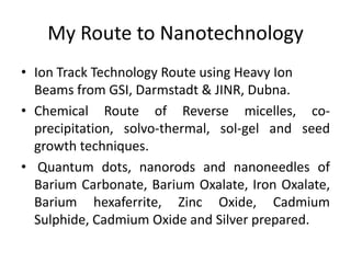
Ion Track Technology [1] was developed at GSI,
Darmstadt. Ion Track Filters (ITFs) or Track-etched
membranes became precursors to development of
nanotechnology during 1990s. ITFs were prepared
by bombardment of thin polymer foils using heavy
ions. One of the first applications of ITFs was
separation of cancer blood cells from normal blood
by making use of Nuclepore filters. Author’s group
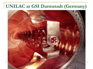
used heavy ion beam facility available at GSI
UNILAC, Darmstadt during 1980s for Ion Beam
Modification of Materials and to prepare ITFs in our
laboratory.
[1] R. Spohr: Ion Tracks and Microtechnology: Principles and Applications
(Vieweg Publications, Weisbaden Germany, 1990)](https://image.slidesharecdn.com/ssntdiontracktechnologytonanotechnology-140417235039-phpapp02/85/Ssntd-ion-track-technology-to-nanotechnology-5-320.jpg)


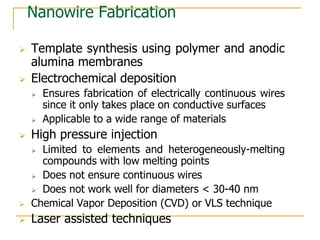
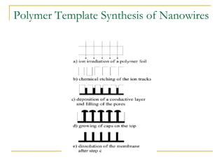
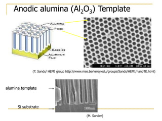


The document chronicles Hardev Singh Virk's transition from ion track technology to nanotechnology, detailing foundational discoveries in nuclear tracks and the development of techniques for creating nanomaterials. It discusses various approaches to nanotechnology, emphasizing the ion track technology route and its applications in the fabrication of nanoparticles and nanostructures. Additionally, the paper highlights methods such as electrochemical deposition and template synthesis for nanowire fabrication, supporting the innovations with acknowledgments of collaborators and facilities involved in the research.


