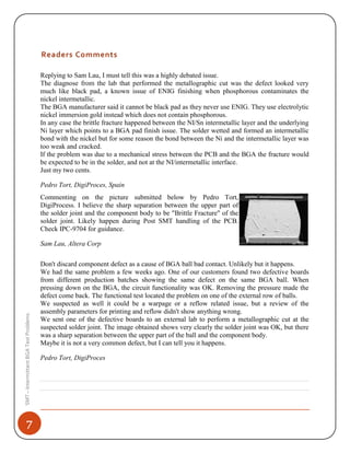
CIRCUITNET
December 26, 2014
Authored by: Circuitnet
Intermittent BGA Test Problems
Expert's Panel Responses
1
SMT–IntermittentBGATestProblems
INTERMITTENT BGA TEST PROBLEMS
We're having problems with some BGA devices after SMT assembly.
During testing the BGA devices are failing, however if we press lightly on the top of the problem BGA device during
testing, the board passes.
What is likely to be the cause? Is it more likely to be solder joint failure, or something internal within the BGA
package?
M.S.
Experts Comments
This sounds like a typical "head-in-pillow" (or "ball-in-socket") defect that is a common issue
with BGAs. In this case, the joint is not really metallurgically formed, but the two metal surfaces
(the solder and the BGA ball) are mechanically touching each other.
The amount of contact between the ball and the solder can vary with the temperature, or with
pressure put onto the part (as you indicated in your question). This is almost certainly not an
internal issue with the component itself; it is a soldering defect at the interface between the ball
and the solder.
There have been a lot of studies conducted and technical papers written on prevention of head-in-
pillow defects. One common cause is the component or board warping just enough that the ball
loses contact with the solder paste just before the paste begins to reflow.
Another cause is that the reflow profile drives a Delta T across the component that can create
some "tilting" of the component, again just enough to let the ball lose contact with the paste just
as the board reaches the liquidus temperature.
This is often a complicated defect resolution, so I would suggest carefully studying the defect
location(s) -- are the defects always occurring on the same parts, same locations on the same
parts? Is it directional -- if you turn the board 180 degrees heading into the oven, does the amount
of locations of the defects change?
I would also suggest to contact your solder paste supplier to see if they have any tips to help with
this. If you contact me directly, I can provide a few papers to help get the process started for
you..
Brian Smith
General Manager - Electronic Assembly Americas
DEK International
Mr. Smith has been supporting customers in the electronics assembly industry since
1994. His expertise is focused on solder paste printing and reducing soldering defects.
He holds a BS in Chemical Engineering and an MBA in Marketing. He has authored several
papers in trade magazines and at industry conferences. He is an SMTA Certified Process
Engineer.
2
SMT–IntermittentBGATestProblems|12/26/2014
You are most likely seeing solder balls underneath the device that did not reflow properly and
therefore are not making electrical connection to their associated pad(s), although there could be
other reasons causing electrical connection failure.
However, in my experience as a contract manufacturer who is exposed to all types of designs this
one is the most probable. Applying pressure on the top of the device during operation is causing
the improperly reflowed solder balls to forcibly make electrical connection. There are a couple of
possible reasons behind the phenomenon that you're seeing but the top three are (and I would
review them in this order):
1. The reflow profile for the board assembly is incorrect and there is not enough heat being
applied to the BGA package to allow the solder balls to reflow properly (perform proper reflow
profiling which is essential especially for large board assemblies);
2. Application of solder paste onto the pads is of insufficient volume to make contact with
the solder balls during reflow (check your solder paste foil thickness and/or aperture design to
ensure that sufficient paste is being applied);
3. Check the planarity of the board fabrication itself, and make certain that there is no
warpage, bow and/or twist (IPC-610 has an equation and specification for this) which will
prevent solder balls on (larger) BGA packages from establishing electrical connectivity during
reflow (this problem is exacerbated when using high-temperature RoHS processing parameters
with thin board fabrications (0.031" or less) built using low Tg materials which essentially causes
to the glass to melt and then reform again introducing bow & twist during the reflow process).
There are other factors that can contribute to this issue that are easily overlooked such as
contaminated or improperly processed board fabrication plating, not storing or handling plastic-
encapsulated high MSL-rated BGA components properly which could cause intermittent package
failure after reflow through outgassing, etc. but the three main issues that I mentioned above
would be the most appropriate starting point to help resolve your issue.
David Bonito
Sales & Marketing Manager
Technical Manufacturing Corp.
David has been active in all areas of the contract electronics manufacturing industry for
over fifteen years. He is currently in charge of all Sales and Marketing related activities
for Technical Manufacturing Corporation.
This would seem to be a classic example of what is known as head in pillow failure.
3
SMT–IntermittentBGATestProblems
The effect is traditionally caused by the volume of solder paste, and therefore the flux being too
low.
During the reflow process due to the low volume of flux, the activity or fluxing action is used up
before the solder powder reaches melting temperature. This reduces the ability of the solder to
break the surface tension or wet to the surface of the BGA ball and causes a reflowed solder pad
in contact, but not soldered to the BGA ball. It will create a contact joint, but not a soldered joint.
The upshot of this is that there is initially some conductance or only conductance if pressure is
applied. On the long term this contact will deteriorate due to oxidation.
The best way to improve this effect is to ensure a better or more consistent volume of solder
paste that is printed to reduce the risk of insufficient volume or look at improving the reflow
profile to reduce the stress or risk of drying out the flux before reflow.
The other potential cause is PCB warpage of the BGA during reflow. If the BGA warps up, there
is a risk that both, ball and solder, reflow as normal, but they are not in contact due to warpage.
As the solder solidifies during cooling down of the reflow profile, they then come into or near to
contact.
This means that during test when pressure is applied you achieve contact and get a pass, but in
realty there is a gap and no contact is made. Again modifying or checking the reflow
temperatures can help reduce this risk.
A simple cross section or in some cases an x-ray may help to show to the root cause.
Doug Dixon
Global Marketing Director
Henkel Electronics
Mr. Dixon has been in the electronics field for over twenty years and is the Global
Marketing Director with the electronics group of Henkel. Prior to joining Henkel, he
worked for Raytheon, Camalot Systems, and Universal Instruments.
This sounds to me like a textbook case of Head-in-Pillow (HiP) defects. What happens in this
4
SMT–IntermittentBGATestProblems|12/26/2014
case is that during reflow, the BGA warps, causing some of the balls to lift out of the paste. The
paste and ball then melt separately.
During cool-down the BGA relaxes and the ball then rests on the reflowed paste, but because of
oxide buildup on the surfaces of both the ball and the paste, combined with a flux that no longer
is active enough to clean the surfaces, the ball and paste do not coalesce together. This causes the
joint to be conductive when in contact, but a slight shift can cause failure of the joint.
It seems that if you are able to press down on the BGA and cause it to work again, HiP is your
cause. It's hard to diagnose this for sure without tearing off a BGA or two and looking to see if
the joints on the corners are well formed, because in a top-down x-ray the joint will look normal.
For more information here is a link to a paper by a colleague of mine.
Brook Sandy
Product Support Specialist
Indium Corporation
Brook is Product Support Specialist for PCB Assembly Materials at Indium Corp.
With a background in Chemical Engineering and previous experience with conductive
adhesive new product development, she provides expertise in choosing the right
materials and processes to optimize PCB assembly operations.
Most likely cause is a Head on Pillow (HoP) joint failure under the BGA, where the solder paste
and the BGA solder ball are not merged, or in contact, following reflow. Downward pressure on
the BGA makes an electrical contact on the joint, which releases as the finger pressure is
removed and the failure re-establishes.
An x-ray view at an oblique angle should confirm this non-destructively as the ball and the paste
will appear as distinct separate entities compared with a single entity that would be a correctly re-
flowed ball. An example image is attached - note the variation in the ball shapes - indicating an
uneven response to the reflow and the Head on Pillow joints having the separate 'shadow' like
structure with respect to the solder ball.
If x-ray inspection shows that all of the BGA joints are consistent then this failure is not due to
Head on Pillow joints and it could be caused by warpage of the device cracking and lifting the
device away from the board. Alternatively, it could be through a failure within the BGA package
itself where an internal joint has failed and pressure applied, again, re-makes the joint.
Dr. David Bernard
Product Manager
Dage Precision Industries
Mr. Bernard has been the X-ray Systems Product Manager at Dage for over 5 years
and have been involved in all aspects of x-ray inspection and test for printed circuit
board assembly applications. Prior to this, Dr. Bernard was working with radiation
measurement instrumentation.
I expect the most likely cause to be open solder joints below the BGA device. Pressing down on
5
SMT–IntermittentBGATestProblems
top of the package provides temporary contact.
The likely root cause is warpage of the BGA or the board during reflow. Oftentimes, this will be
resolved by extending preheat or slowing the ramp rates in your reflow profile, allowing some
stress relief.
A less likely cause is delamination of BGA due to moisture. Adequate pre-bake should resolve
this issue.
Don Naugler
General Manager
VJ Technologies, Inc.
Don is the General Manager of VJ Technologies, Inc., a leading manufacturer of X-
ray Inspection and Rework equipment for the electronics manufacturing industry. He
has more than 20 years experience in development, manufacturing, and support of a
wide range of capital equipment.
Assuming the BGA components are good, it sounds like a reflow profile that is either too hot or
too cold. I would instrument the PCB and run it thru the oven.
Once this is completed, you will have a better understanding of which direction to take.
Edward Zamborsky
Regional Sales Manager
OK International Inc.
Mr. Zamborsky serves as one of OK's technology advisers to the Product Development
group. Ed has authored articles and papers on topics such as; Low Volume SMT
Assembly, Solder Fume Extraction, SMT Rework, BGA Rework, Lead Free Hand
Soldering, Lead Free Visual Inspection and Lead Free Array Rework.
6
SMT–IntermittentBGATestProblems|12/26/2014
If I would create a list related to this it would include (note: in random order):
• Oven profile related: head in pillow, improper reflow profile - too hot, too cold, is the
profile following the solder paste manufacturer's recommendations.
• Micro cracks in the solder joints
• Other soldering issues - what is the processing time - is there enough time to allow the
flux solvents to evaporate, causing an improper wetting?
• Assembly line - is there any vibrations on your reflow oven rails? What about your wave
- other than mechanical stress, is there enough heat to reflow the BGA on the top side (if the
board is mixed technology and goes through a wave or selective soldering)
• What is the cleaning process? If you perform a wash cycle, how much time do you allow
the assembly to cool down after reflow before cleaning? Do you measure the temperature of the
assmebly before cleaning?
• Insufficient solder - stencil design,paste type, paste deposition related issues: accuracy,
clogged apertures, cleaning
• Component issues: solder ball separating from the body of the component, MSD stored
improperly, contamination (finger prints???)
• PCB issues: board flexing, separation in between layers, pad related issue (finish), bad
pad design, contamination (finger prints???, Are there via holes around the pads that the solder
can wick into. How accurate is the solder resist applied around the pads?
• Last but not least, I wouldn't ever rule out the human factor - there is always a failure that
I call MOE (Major Operator Error)
I hope this helps.
Georgian Simion
Engineering and Operations Management
Independent Consultant
Georgian Simion is an independent consultant with 20+ years in electronics
manufacturing engineering and operations.
7
SMT–IntermittentBGATestProblems
Readers Comments
Replying to Sam Lau, I must tell this was a highly debated issue.
The diagnose from the lab that performed the metallographic cut was the defect looked very
much like black pad, a known issue of ENIG finishing when phosphorous contaminates the
nickel intermetallic.
The BGA manufacturer said it cannot be black pad as they never use ENIG. They use electrolytic
nickel immersion gold instead which does not contain phosphorous.
In any case the brittle fracture happened between the NI/Sn intermetallic layer and the underlying
Ni layer which points to a BGA pad finish issue. The solder wetted and formed an intermetallic
bond with the nickel but for some reason the bond between the Ni and the intermetallic layer was
too weak and cracked.
If the problem was due to a mechanical stress between the PCB and the BGA the fracture would
be expected to be in the solder, and not at the NI/intermetallic interface.
Just my two cents.
Pedro Tort, DigiProces, Spain
Commenting on the picture submitted below by Pedro Tort,
DigiProcess. I believe the sharp separation between the upper part of
the solder joint and the component body to be "Brittle Fracture" of the
solder joint. Likely happen during Post SMT handling of the PCB.
Check IPC-9704 for guidance.
Sam Lau, Altera Corp
Don't discard component defect as a cause of BGA ball bad contact. Unlikely but it happens.
We had the same problem a few weeks ago. One of our customers found two defective boards
from different production batches showing the same defect on the same BGA ball. When
pressing down on the BGA, the circuit functionality was OK. Removing the pressure made the
defect come back. The functional test located the problem on one of the external row of balls.
We suspected as well it could be a warpage or a reflow related issue, but a review of the
assembly parameters for printing and reflow didn't show anything wrong.
We sent one of the defective boards to an external lab to perform a metallographic cut at the
suspected solder joint. The image obtained shows very clearly the solder joint was OK, but there
was a sharp separation between the upper part of the ball and the component body.
Maybe it is not a very common defect, but I can tell you it happens.
Pedro Tort, DigiProces

SMT - Intermittent BGA Test Problems

  • 1.
    CIRCUITNET December 26, 2014 Authoredby: Circuitnet Intermittent BGA Test Problems Expert's Panel Responses
  • 2.
    1 SMT–IntermittentBGATestProblems INTERMITTENT BGA TESTPROBLEMS We're having problems with some BGA devices after SMT assembly. During testing the BGA devices are failing, however if we press lightly on the top of the problem BGA device during testing, the board passes. What is likely to be the cause? Is it more likely to be solder joint failure, or something internal within the BGA package? M.S. Experts Comments This sounds like a typical "head-in-pillow" (or "ball-in-socket") defect that is a common issue with BGAs. In this case, the joint is not really metallurgically formed, but the two metal surfaces (the solder and the BGA ball) are mechanically touching each other. The amount of contact between the ball and the solder can vary with the temperature, or with pressure put onto the part (as you indicated in your question). This is almost certainly not an internal issue with the component itself; it is a soldering defect at the interface between the ball and the solder. There have been a lot of studies conducted and technical papers written on prevention of head-in- pillow defects. One common cause is the component or board warping just enough that the ball loses contact with the solder paste just before the paste begins to reflow. Another cause is that the reflow profile drives a Delta T across the component that can create some "tilting" of the component, again just enough to let the ball lose contact with the paste just as the board reaches the liquidus temperature. This is often a complicated defect resolution, so I would suggest carefully studying the defect location(s) -- are the defects always occurring on the same parts, same locations on the same parts? Is it directional -- if you turn the board 180 degrees heading into the oven, does the amount of locations of the defects change? I would also suggest to contact your solder paste supplier to see if they have any tips to help with this. If you contact me directly, I can provide a few papers to help get the process started for you.. Brian Smith General Manager - Electronic Assembly Americas DEK International Mr. Smith has been supporting customers in the electronics assembly industry since 1994. His expertise is focused on solder paste printing and reducing soldering defects. He holds a BS in Chemical Engineering and an MBA in Marketing. He has authored several papers in trade magazines and at industry conferences. He is an SMTA Certified Process Engineer.
  • 3.
    2 SMT–IntermittentBGATestProblems|12/26/2014 You are mostlikely seeing solder balls underneath the device that did not reflow properly and therefore are not making electrical connection to their associated pad(s), although there could be other reasons causing electrical connection failure. However, in my experience as a contract manufacturer who is exposed to all types of designs this one is the most probable. Applying pressure on the top of the device during operation is causing the improperly reflowed solder balls to forcibly make electrical connection. There are a couple of possible reasons behind the phenomenon that you're seeing but the top three are (and I would review them in this order): 1. The reflow profile for the board assembly is incorrect and there is not enough heat being applied to the BGA package to allow the solder balls to reflow properly (perform proper reflow profiling which is essential especially for large board assemblies); 2. Application of solder paste onto the pads is of insufficient volume to make contact with the solder balls during reflow (check your solder paste foil thickness and/or aperture design to ensure that sufficient paste is being applied); 3. Check the planarity of the board fabrication itself, and make certain that there is no warpage, bow and/or twist (IPC-610 has an equation and specification for this) which will prevent solder balls on (larger) BGA packages from establishing electrical connectivity during reflow (this problem is exacerbated when using high-temperature RoHS processing parameters with thin board fabrications (0.031" or less) built using low Tg materials which essentially causes to the glass to melt and then reform again introducing bow & twist during the reflow process). There are other factors that can contribute to this issue that are easily overlooked such as contaminated or improperly processed board fabrication plating, not storing or handling plastic- encapsulated high MSL-rated BGA components properly which could cause intermittent package failure after reflow through outgassing, etc. but the three main issues that I mentioned above would be the most appropriate starting point to help resolve your issue. David Bonito Sales & Marketing Manager Technical Manufacturing Corp. David has been active in all areas of the contract electronics manufacturing industry for over fifteen years. He is currently in charge of all Sales and Marketing related activities for Technical Manufacturing Corporation. This would seem to be a classic example of what is known as head in pillow failure.
  • 4.
    3 SMT–IntermittentBGATestProblems The effect istraditionally caused by the volume of solder paste, and therefore the flux being too low. During the reflow process due to the low volume of flux, the activity or fluxing action is used up before the solder powder reaches melting temperature. This reduces the ability of the solder to break the surface tension or wet to the surface of the BGA ball and causes a reflowed solder pad in contact, but not soldered to the BGA ball. It will create a contact joint, but not a soldered joint. The upshot of this is that there is initially some conductance or only conductance if pressure is applied. On the long term this contact will deteriorate due to oxidation. The best way to improve this effect is to ensure a better or more consistent volume of solder paste that is printed to reduce the risk of insufficient volume or look at improving the reflow profile to reduce the stress or risk of drying out the flux before reflow. The other potential cause is PCB warpage of the BGA during reflow. If the BGA warps up, there is a risk that both, ball and solder, reflow as normal, but they are not in contact due to warpage. As the solder solidifies during cooling down of the reflow profile, they then come into or near to contact. This means that during test when pressure is applied you achieve contact and get a pass, but in realty there is a gap and no contact is made. Again modifying or checking the reflow temperatures can help reduce this risk. A simple cross section or in some cases an x-ray may help to show to the root cause. Doug Dixon Global Marketing Director Henkel Electronics Mr. Dixon has been in the electronics field for over twenty years and is the Global Marketing Director with the electronics group of Henkel. Prior to joining Henkel, he worked for Raytheon, Camalot Systems, and Universal Instruments. This sounds to me like a textbook case of Head-in-Pillow (HiP) defects. What happens in this
  • 5.
    4 SMT–IntermittentBGATestProblems|12/26/2014 case is thatduring reflow, the BGA warps, causing some of the balls to lift out of the paste. The paste and ball then melt separately. During cool-down the BGA relaxes and the ball then rests on the reflowed paste, but because of oxide buildup on the surfaces of both the ball and the paste, combined with a flux that no longer is active enough to clean the surfaces, the ball and paste do not coalesce together. This causes the joint to be conductive when in contact, but a slight shift can cause failure of the joint. It seems that if you are able to press down on the BGA and cause it to work again, HiP is your cause. It's hard to diagnose this for sure without tearing off a BGA or two and looking to see if the joints on the corners are well formed, because in a top-down x-ray the joint will look normal. For more information here is a link to a paper by a colleague of mine. Brook Sandy Product Support Specialist Indium Corporation Brook is Product Support Specialist for PCB Assembly Materials at Indium Corp. With a background in Chemical Engineering and previous experience with conductive adhesive new product development, she provides expertise in choosing the right materials and processes to optimize PCB assembly operations. Most likely cause is a Head on Pillow (HoP) joint failure under the BGA, where the solder paste and the BGA solder ball are not merged, or in contact, following reflow. Downward pressure on the BGA makes an electrical contact on the joint, which releases as the finger pressure is removed and the failure re-establishes. An x-ray view at an oblique angle should confirm this non-destructively as the ball and the paste will appear as distinct separate entities compared with a single entity that would be a correctly re- flowed ball. An example image is attached - note the variation in the ball shapes - indicating an uneven response to the reflow and the Head on Pillow joints having the separate 'shadow' like structure with respect to the solder ball. If x-ray inspection shows that all of the BGA joints are consistent then this failure is not due to Head on Pillow joints and it could be caused by warpage of the device cracking and lifting the device away from the board. Alternatively, it could be through a failure within the BGA package itself where an internal joint has failed and pressure applied, again, re-makes the joint. Dr. David Bernard Product Manager Dage Precision Industries Mr. Bernard has been the X-ray Systems Product Manager at Dage for over 5 years and have been involved in all aspects of x-ray inspection and test for printed circuit board assembly applications. Prior to this, Dr. Bernard was working with radiation measurement instrumentation. I expect the most likely cause to be open solder joints below the BGA device. Pressing down on
  • 6.
    5 SMT–IntermittentBGATestProblems top of thepackage provides temporary contact. The likely root cause is warpage of the BGA or the board during reflow. Oftentimes, this will be resolved by extending preheat or slowing the ramp rates in your reflow profile, allowing some stress relief. A less likely cause is delamination of BGA due to moisture. Adequate pre-bake should resolve this issue. Don Naugler General Manager VJ Technologies, Inc. Don is the General Manager of VJ Technologies, Inc., a leading manufacturer of X- ray Inspection and Rework equipment for the electronics manufacturing industry. He has more than 20 years experience in development, manufacturing, and support of a wide range of capital equipment. Assuming the BGA components are good, it sounds like a reflow profile that is either too hot or too cold. I would instrument the PCB and run it thru the oven. Once this is completed, you will have a better understanding of which direction to take. Edward Zamborsky Regional Sales Manager OK International Inc. Mr. Zamborsky serves as one of OK's technology advisers to the Product Development group. Ed has authored articles and papers on topics such as; Low Volume SMT Assembly, Solder Fume Extraction, SMT Rework, BGA Rework, Lead Free Hand Soldering, Lead Free Visual Inspection and Lead Free Array Rework.
  • 7.
    6 SMT–IntermittentBGATestProblems|12/26/2014 If I wouldcreate a list related to this it would include (note: in random order): • Oven profile related: head in pillow, improper reflow profile - too hot, too cold, is the profile following the solder paste manufacturer's recommendations. • Micro cracks in the solder joints • Other soldering issues - what is the processing time - is there enough time to allow the flux solvents to evaporate, causing an improper wetting? • Assembly line - is there any vibrations on your reflow oven rails? What about your wave - other than mechanical stress, is there enough heat to reflow the BGA on the top side (if the board is mixed technology and goes through a wave or selective soldering) • What is the cleaning process? If you perform a wash cycle, how much time do you allow the assembly to cool down after reflow before cleaning? Do you measure the temperature of the assmebly before cleaning? • Insufficient solder - stencil design,paste type, paste deposition related issues: accuracy, clogged apertures, cleaning • Component issues: solder ball separating from the body of the component, MSD stored improperly, contamination (finger prints???) • PCB issues: board flexing, separation in between layers, pad related issue (finish), bad pad design, contamination (finger prints???, Are there via holes around the pads that the solder can wick into. How accurate is the solder resist applied around the pads? • Last but not least, I wouldn't ever rule out the human factor - there is always a failure that I call MOE (Major Operator Error) I hope this helps. Georgian Simion Engineering and Operations Management Independent Consultant Georgian Simion is an independent consultant with 20+ years in electronics manufacturing engineering and operations.
  • 8.
    7 SMT–IntermittentBGATestProblems Readers Comments Replying toSam Lau, I must tell this was a highly debated issue. The diagnose from the lab that performed the metallographic cut was the defect looked very much like black pad, a known issue of ENIG finishing when phosphorous contaminates the nickel intermetallic. The BGA manufacturer said it cannot be black pad as they never use ENIG. They use electrolytic nickel immersion gold instead which does not contain phosphorous. In any case the brittle fracture happened between the NI/Sn intermetallic layer and the underlying Ni layer which points to a BGA pad finish issue. The solder wetted and formed an intermetallic bond with the nickel but for some reason the bond between the Ni and the intermetallic layer was too weak and cracked. If the problem was due to a mechanical stress between the PCB and the BGA the fracture would be expected to be in the solder, and not at the NI/intermetallic interface. Just my two cents. Pedro Tort, DigiProces, Spain Commenting on the picture submitted below by Pedro Tort, DigiProcess. I believe the sharp separation between the upper part of the solder joint and the component body to be "Brittle Fracture" of the solder joint. Likely happen during Post SMT handling of the PCB. Check IPC-9704 for guidance. Sam Lau, Altera Corp Don't discard component defect as a cause of BGA ball bad contact. Unlikely but it happens. We had the same problem a few weeks ago. One of our customers found two defective boards from different production batches showing the same defect on the same BGA ball. When pressing down on the BGA, the circuit functionality was OK. Removing the pressure made the defect come back. The functional test located the problem on one of the external row of balls. We suspected as well it could be a warpage or a reflow related issue, but a review of the assembly parameters for printing and reflow didn't show anything wrong. We sent one of the defective boards to an external lab to perform a metallographic cut at the suspected solder joint. The image obtained shows very clearly the solder joint was OK, but there was a sharp separation between the upper part of the ball and the component body. Maybe it is not a very common defect, but I can tell you it happens. Pedro Tort, DigiProces