This document provides a 116-page report on the semiconductor equipment industry in 2009. It summarizes the drastic decline in the industry from 2007 to 2009, with nearly all manufacturers seeing less than half of their 2007 revenue levels. The report analyzes market trends for various semiconductor equipment manufacturers and segments, including lithography, wafer fabrication, memory, and IDM. It also profiles the top 20 semiconductor equipment companies and examines their financial performance over this period.
Global and china rigid pcb industry report, 2015ResearchInChina
2014 was a good year for majority of PCB companies, as output value of PCB industry touched USD59.6 billion, rising 3.7% against 2013, the fastest growth rate since 2011. Looking forward to 2015, a collapse in prices of commodities, especially in that of copper, will significantly reduce raw materials costs of PCB companies, thus further driving their profit margins.
Automotive PCB market is the biggest highlight. Global automotive PCB market size was USD5.28 billion in 2015 and is expected to grow by 8.3% to USD5.72 billion in 2016 and by 8.2% to USD6.19 billion in 2017, primarily because of impetus of millimeter-wave radar to RF board, of connected vehicle to multi-layer board, and of chassis electronization to metal substrate.
Global and china ic substrate industry report, 2015ResearchInChina
IC substrate industry may be in a predicament in 2015, rooted in two aspects: first, the maturing of FOWLP; second, the tablet sales decline and sluggish smartphone growth. In addition, the prosperity of IC substrate industry in 2013 stimulated large-scale expansion of enterprises in 2014, thus leading to an insufficient rate of capacity utilization.
LIANG Zheng: Comparison of China and India in R&D globalisationSTEPS Centre
LIANG Zheng, Associate Professor, CISTP, Tsinghua University.
Presentation to the UK-China Innovation Workshop for Sustainable and Equitable Development, Tsinghua University, 19 March 2010, co-organised by China Institute for Science and Technology Policy (CISTP) at Tsinghua University and the STEPS Centre.
http://anewmanifesto.org/news/china-workshop-presentationschina-workshop-presentations/
Stellar and laboratory XUV/EUV line ratios in Fe XVIII and Fe XIXAstroAtom
Talk given by E. Träbert, P. Beiersdorfer , J. Clementson at the 17th International Conference on Atomic Processes in Plasmas, Belfast, UK, 19-22 July 2011.
Multiple patterning is a class of technologies for manufacturing integrated circuits (ICs), developed for photolithography to enhance the feature density. The simplest case of multiple patterning is double patterning, where a conventional lithography process is enhanced to produce double the expected number of features. The resolution of a photoresist pattern is believed to blur at around 45 nm half-pitch. For the semiconductor industry, therefore, double patterning was introduced for the 32 nm half-pitch node and below. This presentation gives us an insight of why multiple patterning is an important to give us a better resolution below 32nm.
Introduction to VLSI, Scaling, CMOS technology, Source and sinks, Operational Amplifiers, Noise, MOS inverter, Synchronous circuits, Design verification and testing
Xavi is professional EMS factory ,products include PON,STB, WIFI module,IOT,IPC..,etc. For more detail information, Please contact with yc_pan@xavi.com.tw
(Company profile)ykt pcb manufacturer_in_korea_2019_1st_halfPark Jin Young
Now, the U.S. and China traded war is getting worse and worse.
It is time to re-consider your PCB supply chain in order to overcome the unforeseeable global trading circumstance.
If you are looking for a reliable PCB manufacturer in Korea, we guarantee that we can be your alternative option for your Business Continuity Management Plan.
If you are interested in purchasing PCB from Korea, please do't hesitate to contact me.
Presented at a SAP industry conference, this deck talks about how High Tech companies can transform their supply networks via performance management, collaborative planning, and network planning & execution
How to Make a Field invisible in Odoo 17Celine George
It is possible to hide or invisible some fields in odoo. Commonly using “invisible” attribute in the field definition to invisible the fields. This slide will show how to make a field invisible in odoo 17.
June 3, 2024 Anti-Semitism Letter Sent to MIT President Kornbluth and MIT Cor...Levi Shapiro
Letter from the Congress of the United States regarding Anti-Semitism sent June 3rd to MIT President Sally Kornbluth, MIT Corp Chair, Mark Gorenberg
Dear Dr. Kornbluth and Mr. Gorenberg,
The US House of Representatives is deeply concerned by ongoing and pervasive acts of antisemitic
harassment and intimidation at the Massachusetts Institute of Technology (MIT). Failing to act decisively to ensure a safe learning environment for all students would be a grave dereliction of your responsibilities as President of MIT and Chair of the MIT Corporation.
This Congress will not stand idly by and allow an environment hostile to Jewish students to persist. The House believes that your institution is in violation of Title VI of the Civil Rights Act, and the inability or
unwillingness to rectify this violation through action requires accountability.
Postsecondary education is a unique opportunity for students to learn and have their ideas and beliefs challenged. However, universities receiving hundreds of millions of federal funds annually have denied
students that opportunity and have been hijacked to become venues for the promotion of terrorism, antisemitic harassment and intimidation, unlawful encampments, and in some cases, assaults and riots.
The House of Representatives will not countenance the use of federal funds to indoctrinate students into hateful, antisemitic, anti-American supporters of terrorism. Investigations into campus antisemitism by the Committee on Education and the Workforce and the Committee on Ways and Means have been expanded into a Congress-wide probe across all relevant jurisdictions to address this national crisis. The undersigned Committees will conduct oversight into the use of federal funds at MIT and its learning environment under authorities granted to each Committee.
• The Committee on Education and the Workforce has been investigating your institution since December 7, 2023. The Committee has broad jurisdiction over postsecondary education, including its compliance with Title VI of the Civil Rights Act, campus safety concerns over disruptions to the learning environment, and the awarding of federal student aid under the Higher Education Act.
• The Committee on Oversight and Accountability is investigating the sources of funding and other support flowing to groups espousing pro-Hamas propaganda and engaged in antisemitic harassment and intimidation of students. The Committee on Oversight and Accountability is the principal oversight committee of the US House of Representatives and has broad authority to investigate “any matter” at “any time” under House Rule X.
• The Committee on Ways and Means has been investigating several universities since November 15, 2023, when the Committee held a hearing entitled From Ivory Towers to Dark Corners: Investigating the Nexus Between Antisemitism, Tax-Exempt Universities, and Terror Financing. The Committee followed the hearing with letters to those institutions on January 10, 202
Acetabularia Information For Class 9 .docxvaibhavrinwa19
Acetabularia acetabulum is a single-celled green alga that in its vegetative state is morphologically differentiated into a basal rhizoid and an axially elongated stalk, which bears whorls of branching hairs. The single diploid nucleus resides in the rhizoid.
A Strategic Approach: GenAI in EducationPeter Windle
Artificial Intelligence (AI) technologies such as Generative AI, Image Generators and Large Language Models have had a dramatic impact on teaching, learning and assessment over the past 18 months. The most immediate threat AI posed was to Academic Integrity with Higher Education Institutes (HEIs) focusing their efforts on combating the use of GenAI in assessment. Guidelines were developed for staff and students, policies put in place too. Innovative educators have forged paths in the use of Generative AI for teaching, learning and assessments leading to pockets of transformation springing up across HEIs, often with little or no top-down guidance, support or direction.
This Gasta posits a strategic approach to integrating AI into HEIs to prepare staff, students and the curriculum for an evolving world and workplace. We will highlight the advantages of working with these technologies beyond the realm of teaching, learning and assessment by considering prompt engineering skills, industry impact, curriculum changes, and the need for staff upskilling. In contrast, not engaging strategically with Generative AI poses risks, including falling behind peers, missed opportunities and failing to ensure our graduates remain employable. The rapid evolution of AI technologies necessitates a proactive and strategic approach if we are to remain relevant.
Read| The latest issue of The Challenger is here! We are thrilled to announce that our school paper has qualified for the NATIONAL SCHOOLS PRESS CONFERENCE (NSPC) 2024. Thank you for your unwavering support and trust. Dive into the stories that made us stand out!
Operation “Blue Star” is the only event in the history of Independent India where the state went into war with its own people. Even after about 40 years it is not clear if it was culmination of states anger over people of the region, a political game of power or start of dictatorial chapter in the democratic setup.
The people of Punjab felt alienated from main stream due to denial of their just demands during a long democratic struggle since independence. As it happen all over the word, it led to militant struggle with great loss of lives of military, police and civilian personnel. Killing of Indira Gandhi and massacre of innocent Sikhs in Delhi and other India cities was also associated with this movement.
Instructions for Submissions thorugh G- Classroom.pptxJheel Barad
This presentation provides a briefing on how to upload submissions and documents in Google Classroom. It was prepared as part of an orientation for new Sainik School in-service teacher trainees. As a training officer, my goal is to ensure that you are comfortable and proficient with this essential tool for managing assignments and fostering student engagement.
Biological screening of herbal drugs: Introduction and Need for
Phyto-Pharmacological Screening, New Strategies for evaluating
Natural Products, In vitro evaluation techniques for Antioxidants, Antimicrobial and Anticancer drugs. In vivo evaluation techniques
for Anti-inflammatory, Antiulcer, Anticancer, Wound healing, Antidiabetic, Hepatoprotective, Cardio protective, Diuretics and
Antifertility, Toxicity studies as per OECD guidelines
Unit 8 - Information and Communication Technology (Paper I).pdfThiyagu K
This slides describes the basic concepts of ICT, basics of Email, Emerging Technology and Digital Initiatives in Education. This presentations aligns with the UGC Paper I syllabus.
2024.06.01 Introducing a competency framework for languag learning materials ...Sandy Millin
http://sandymillin.wordpress.com/iateflwebinar2024
Published classroom materials form the basis of syllabuses, drive teacher professional development, and have a potentially huge influence on learners, teachers and education systems. All teachers also create their own materials, whether a few sentences on a blackboard, a highly-structured fully-realised online course, or anything in between. Despite this, the knowledge and skills needed to create effective language learning materials are rarely part of teacher training, and are mostly learnt by trial and error.
Knowledge and skills frameworks, generally called competency frameworks, for ELT teachers, trainers and managers have existed for a few years now. However, until I created one for my MA dissertation, there wasn’t one drawing together what we need to know and do to be able to effectively produce language learning materials.
This webinar will introduce you to my framework, highlighting the key competencies I identified from my research. It will also show how anybody involved in language teaching (any language, not just English!), teacher training, managing schools or developing language learning materials can benefit from using the framework.
2024.06.01 Introducing a competency framework for languag learning materials ...
Semiconductor equipment industry report, 2009
1. 168Report-China Market Research Reports
Semiconductor Equipment Industry Report, 2009
Hard copy : 2100 USD
Electronic copy (PDF) : 23000USD
Hard and Electronic copy : 3400USD
Pages: 116
Tables and figures :
Published date :Nov, 2009
Publisher: 168Report
Contact: Mr. Peter Lee +86-10-82965190 +86-13161572746 sales@168report.com
Abstract
The drastic fluctuations in semiconductor industry are astonishing. NAND flash memory stood out
conspicuously during the period of 2005-2007, the shipment boosted up, and manufacturers
successively invested in NAND field. The emerging DDR2 was once promoted greatly by
Microsoft Vista. In wafer OEM, a fierce competition on advanced manufacturing process is under
way, and the manufacturers all have continuously pushed forward 90nm and 65nm, so the
shipment of semiconductor equipments increased considerably. The coming into being of new
packaging forms such as FC, CSP, and WLP also conduced to the development of semiconductor
equipment industry. Therefore, the period from 2005 to 2007 was the boom for semiconductor
industry, and many manufacturers doubled their revenue. However, while they were in high
spirits, the semiconductor industry had started to plunge.
The decline in 2008 was just the beginning, the year of 2009 witnessed more dramatically drop,
and the revenue of nearly all the manufacturers was less than 50% of the level in 2007, or even
20%. Especially lithography industry in the front-end area of semiconductor equipment, the top
three manufacturers, ASML, NIKON and CANON, respectively fell by 44%, 73% and 84%.
Almost all the manufacturers have suffered the loss.
It was a bit better for the manufacturers in the back-end field of semiconductor equipment
industry, particularly testing sector, it witnessed a small drop.
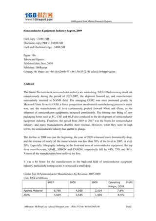
Global Top 20 Semiconductor Manufacturers by Revenue, 2007-2009
Unit: US$ in Millions
2007 2008 2009 Operating Profit
Margin, 2009
Applied Material 6,788 4,088 2,008 7.8%
ASML 4,609 3,525 1,960 -8.5%
168Report Mr.Peter Lee sales@168report.com 13161572746 8610-82965190 Page 1
2. 168Report-China Market Research Reports
Tokyo Electron 5,362 3,453 1,558 -21.0%
KLA-Tencor 2,326 1,771 1,520 -38.0%
Lam Research 2,245 1,502 1,116 25.2%
Nikon 1,806 1,333 488 -23.6%
Carl Zeiss SMT 1,208 1,314 1,068 10%
Dainippon Screen 1,196 832 746
Teradyne 707 825 728 -21.7%
Advantest 1,608 788 340 -37.7%
ASM International 1,023 787 519 -24.7%
Hitachi High-
Technologies
960 711 688 -24.0%
Novellus system 1,200 703 398 -19.4%
Canon 784 608 98
Varian 863 491 362 -11.9%
Verigy 633 464 336 -32.7%
Daifuku 335 402 138
Aixtron 261 366 349 13.2%
Hitachi Kokusai
Electric
618 361 178 -17.4%
Tokyo Semitsu 568 334 128
The situation improved in the second half of 2009, particularly in memory field, the largest market
in semiconductor equipment industry. In IDM sector, Intel is still the largest semiconductor
equipment client. Since semiconductor equipment industry is lack of unparalleled applications,
revolutionary products and technologies, so it is not likely that the rapid growth during 2005-2007
will come back.
Contents
1 Semiconductor Industry
1.1 Current Situation
1.2 Semiconductor Equipment
1.3 EUV vs. ArF
1.4 15-inch Wafer
2 Semiconductor Equipment Industry and Market
2.1 Semiconductor Equipment Market
2.2 Wafer Semiconductor Equipment Market
2.3 Global Semiconductor Market by Region
3 Semiconductor Equipment Industry
168Report Mr.Peter Lee sales@168report.com 13161572746 8610-82965190 Page 2
3. 168Report-China Market Research Reports
3.1 Overview
3.2 Regional Distribution
3.2.1 Taiwan
3.2.2 Mainland, China
3.3 Automatic Testing
3.4 Etching
4 Semiconductor Equipment Downstream Market
4.1 Wafer OEM
4.1.1 Status Quo
4.1.2 Capital Expenditure
4.1.3 GlobalFoundries
4.1.4 TSMC
4.1.5 UMC
4.1.6 SMIC
4.2 Memory Industry
4.2.1 NAND
4.2.2 Toshiba
4.2.4 DRAM
4.2.5 HYNIX and Samsung Process Progress
4.2.6 DRAM Manufacturers’ Expenses, 2010
4.3 IDM
4.4 Packaging & Testing Industry
5 Semiconductor Equipment Manufacturers
5.1 Applied Materials
5.2 ASML
5.3 KLA-Tencor
5.4 Hitachi High-Tech
5.5 TEL
5.6 NIKON
5.7 DNS
5.8 AIXTRON
5.9 ADVANTEST
5.10 LamResearch
5.11 Zeiss SMT
5.12 Teradyne
5.13 Novellus
5.14 Verigy
5.15 Varian
5.16 Hitachi Kokusai Electric
5.17 ASM International
5.18 Canon
168Report Mr.Peter Lee sales@168report.com 13161572746 8610-82965190 Page 3
4. 168Report-China Market Research Reports
Selected Charts
Ratio of Global Semiconductor Order to Shipment, Jan, 1997-Jul, 2009
Ratio of Order to Shipment of North American Semiconductor Manufacturers, Jan, 2007-Sep,
2009
IC Design Industry Chain
Wafer Manufacturing Flow
Global Semiconductor Equipment Market Size, 2006-2012E
Global Semiconductor Equipment Capital Expenditure, 1987-2010E
Global Semiconductor Materials Revenue, 1987-2010E
Construction Investment of Global Wafer Fabs, 2008Q1-2010Q4E
Equipment Investment of Global Wafer Fabs, 2008Q1-2010Q4E
Investments of Global Wafer Fabs, 2008Q1-2010Q4E
Global Equivalent 8-inch Wafer Output Capacity by Downstream Product Type, 1998-2010E
Output Capacity Distribution of Global Wafer Fabs, 2008Q1-2010Q4E
Global Semiconductor Market by Region, 2008
Global Semiconductor Market by Region, 2009 vs. 2010 (forecast)
Global Semiconductor Equipment Market by Technology, 2007-2010E
Global Semiconductor Market Distribution by Downstream Application, 2009-2010E
Global Wafer Fabrication Materials Market Size and Regional Distribution, 2008-2009
Global Packaging Plant Materials Market Size and Regional Distribution, 2008-2009
Output Value of Semiconductor Equipment Industry, 2009
Output Value of Semiconductor Industry by Region, 2009
Taiwan Semiconductor Equipment Market by Technology, 2008
Taiwan Semiconductor Equipment Imported Value by Country, 2008
Global Semiconductor ATE Market by Downstream Application, 2009
Global Semiconductor ATE Market by Region, 2009
Market Shares of Main Global Automatic Testing Manufacturers, 2007
Market Shares of Global Automatic Testing Manufacturers, 2008
Market Shares of Main Semiconductor Etching Equipment Manufacturers, 2005-2008
Wafer Output Capacity Utilization Rate, 2004Q1-2010Q4E
Wafer OEM Industry Revenue, 2008Q1-2010Q4E
Global Main Wafer OEM Output Capacity, 2007-2012E
TSMC Revenue and Operating Profit Margin, 2003-2009
TSMC Revenue and Operating Profit Margin, 2007-2009Q3
TSMC Revenue by Process, 2007Q1-2009Q3
UMC Revenue and Operating Profit Margin, 2000-2009
UMC Revenue by Process, 2007Q4-2009Q3
UMC Output Capacity Change, 2006Q1-2009Q4
SMIC Revenue and Operating Profit Margin, 2003-2009
SMIC Revenue by Process, 2007Q1-2009Q3
NAND and DRAM Manufacturers’ Capital Expenditure, 2005-2013E
16 & 32 GB 4GX8 MLC NAND Price Trend, Nov, 2008-Nov, 2009
168Report Mr.Peter Lee sales@168report.com 13161572746 8610-82965190 Page 4
5. 168Report-China Market Research Reports
Toshiba NAND Distribution by Process, 2009Q2-2010Q3
Time of Global DRAM Manufacturers to Enter DDR3, 2008Q4-2011Q1
HYNIX DRAM Distribution by Process, 2009Q2-2010Q3
HYNIX NAND Distribution by Process, 2009Q2-2010Q3
Samsung RAM Distribution by Process, 2009Q2-2010Q3
Samsung NAND Distribution by Process, 2009Q2-2010Q3
Applied Materials Revenue and Gross Profit Margin, 2004-2009FY
Applied Materials Revenue by Division, 2006-2009FY
Applied Materials Sales and Operating Profit, Q1-Q4, 2009FY
Applied Materials Revenue by Division, Q42009FY
Applied Materials Orders by Region, Q42009FY
Applied Materials Order Sum by Region, 2006FY-Q3 2009FY
Applied Materials Sales by Region, 2006FY-Q3 2009FY
Applied Materials Order Sum by Division, 2006FY-Q3 2009FY
ASML Revenue and Operating Profit Margin, 2004-2009
ASML Quarterly Revenue, 2003-Q32009
ASML Gross Profit Margin and Operation Profit Margin, Q12008-Q32009
ASML Shipment by Technology, Q12008-Q32009
ASML Revenue by Region, Q12008-Q32009
ASML Revenue by Clients, Q12008-Q32009
Backlog Client Distribution, 2008-Q32009
Backlog Regional Distribution, 2008-Q32009
ASML DRAM Equipment Output Capacity Utilization Rate, Jan, 2007-Aug, 2009
ASML NAND Equipment Output Capacity Utilization Rate, Jan, 2007-Aug, 2009
KLA-Tencor Revenue and Operating Profit Margin, 2005-2009FY
KLA-Tencor Revenue by Region, 2007-2009FY
Hitachi Hi-tech Revenue by Division, 2009-2010FY
Hitachi Hi-tech Operating Profit by Division, 2009-2010FY
Hitachi Hi-tech Semiconductor Equipment Revenue by Product, 2009-2010FY
Hitachi Hi-tech Semiconductor Equipment Revenue by Region, 2009-2010FY
TEL Revenue and Operating Profit, 2001FY-2010FY
TEL Revenue and Operating Profit Margin, Q22007FY-Q22010FY
TEL Quarterly Order Sum by Division, Q32000FY-Q32009FY
TEL Revenue by Division, 2009FY-H12010FY
TEL Semiconductor Equipment Revenue by Region, 2009FY-2010FY
TEL FPD/PVE Equipment Revenue by Region, 2009FY-2010FY
TEL Order Balance, Q32007-Q32009
TEL Order Volume by Region, Q32007-Q32009
TEL Semiconductor Equipment Department's Orders by Product Type, Q32005-Q32009
Nikon Revenue and Operating Profit, 2004FY-2010FY
Nikon Precision Revenue and Operating Profit, 2006FY-2010FY
Nikon Precision’s Exposure Machine Semiconductor Sales Volume by Technology, 2008FY-
2010FY
168Report Mr.Peter Lee sales@168report.com 13161572746 8610-82965190 Page 5
6. 168Report-China Market Research Reports
Nikon Precision’s Exposure Machine Semiconductor Sales Volume by Region, 2008FY-2010FY
Nikon Precision’s Flat Panel Display Exposure Machine Sales Volume by Generation, 2008FY-
2010FY
DNS Revenue and Operating Profit, 2004FY-2009FY
DNS Revenue by Division and Operating Profit Margin, Q32008FY -Q22010FY
DNS Order Sum by Division, Q32008FY-Q22010FY
DNS Semiconductor Equipment Revenue by Downstream Application, Q42007FY-Q12010FY
DNS Flat Panel Display Revenue by Generation, Q42008FY-Q22010FY
AXITRON Employee Number, 2003-2008
AXITRON Revenue by Technology, Q1-Q3, 2009
AXITRON Revenue by Downstream Application, Q1-Q3, 2009
AXITRON Revenue by Region, 2006-Q32009
AXITRON Revenue by Downstream Application, 2006-Q32009
ADVENTES Revenue and Operating Profit Margin, 2003FY-2010FY
ADVENTES Revenue and Order, Q32006-Q22009
ADVENTES Order by Division, Q12008FY-Q22009FY
ADVENTES Order by Region, Q12008FY-Q22009FY
ADVANTEST Revenue by Division, Q12008FY-Q22009FY
ADVANTEST Revenue by Region, Q12008FY-Q22009FY
ADVANTEST Expense Distribution, Q12008FY-Q22009FY
LamResearch Revenue and Operating Profit, 2005FY-2009FY
LamResearch Revenue by Region, 2007FY-2009FY
Zeiss SMT Revenue and Client Distribution, 2004FY-2008FY
Teradyne Revenue and Operating Profit, 2004-2009
Teradyne Order by Region, 2006-2008
Teradyne Revenue by Region, 2006-2008
Verigy Revenue and Operating Profit, 2004-2009
Verigy Revenue by Region, 2006-2008
Verigy Revenue by Downstream Application, Q12005-Q32009
Varian Revenue and Operating Profit, 2004FY-2009FY
Varian Revenue by Business, 2006FY-2009FY
Varian Revenue by Region, 2006FY-2008FY
Varian Revenue by Downstream Application, 2006FY-2008FY
Hitachi Kokusai Electric Revenue and Operating Profit, 2005FY-2009FY
Hitachi Kokusai Electric Revenue by Division, 2007FY-2009FY
ASM Front-end and Back-end Revenue, 2006-2009
ASM Revenue and Operating Profit, 2004-2009
ASM Front-End Equipment Revenue by Region, 2006-2008
ASM Back-End Equipment Revenue by Country, 2006-2008
Canon Revenue and Net Profit, 1999FY-2009FY
Canon Revenue by Product, 1999FY-2008FY
Global Top 20 Semiconductor Manufacturers by Revenue, 2007-2009
Rank of Global Wafer OEMs, Q12009
168Report Mr.Peter Lee sales@168report.com 13161572746 8610-82965190 Page 6
7. 168Report-China Market Research Reports
Expenses of Global Wafer OEMs, Q12007-Q42009
TSMC Output Capacity Change, Q12008-Q42009
Profile of UMC's Trans-invested Companies
Profile of SMIC Wafer Fabs
Operating Revenue of NAND Manufacturers, Q2-Q3, 2009
Rank of Global DRAM Memory Manufacturers, Q32009
Taiwan Memory Manufacturers’ Revenue, Q12008-Aug, 2009
Wafer Output of Taiwan Memory Manufacturers, Q12008-Q4 2009
Expense Forecast of Global Main DRAM Manufacturers, 2010
Global Top 20 Semiconductor Companies, Q1-Q3, 2009
Global Top 20 Semiconductor Companies by Capital Expenditure, 2008-2009
Revenue Forecast of Global Top 19 IC Packaging Plants, 2009
ASML's Current Products
KLA-Tencor’s Products
ASM International’s ALD and CVD Products
ASM International’s Packaging Equipment
ASM R&D Staff and Division Location by Field
ASM Production Bases
168Report Mr.Peter Lee sales@168report.com 13161572746 8610-82965190 Page 7