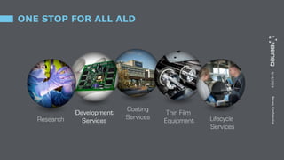
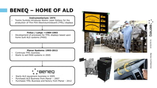
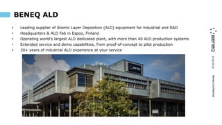
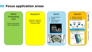
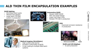
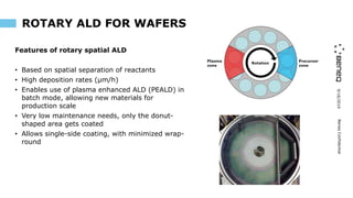
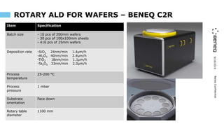
Company confidential
Robust and Reliable Thin-Film OLED
Encapsulation
Bay Area SID Seminar – July 16th 2019
Tommi Kaariainen
9/16/2019BeneqConfidential
• Brief company introduction
• Beneq ALD equipment portfolio
• Beneq ALD technology for moisture barriers and OLED encapsulation
• Discussion
OUTLINE
9/16/2019BeneqConfidential
ONE STOP FOR ALL ALD
9/16/2019BeneqConfidential
BENEQ – HOME OF ALD
• Starts ALD equipment business in 2005
• Purchases ALD Business from Planar – 2007
• Purchases TFEL Business and factory from Planar - 2012
Finlux / Lohja: ~1984-1993
• Development of processes for TFEL displays based upon
home built ALD systems (P400)
Instrumentarium: 1974
• Tuomo Suntola introduces Atomic Layer Epitaxy for the
production of Thin Film Electroluminescent (TFEL) displays
Planar Systems: 1993-2012
• Continues TFEL business.
• Starts to sell P400 systems in 2005
9/16/2019BeneqConfidential
BENEQ ALD
• Leading supplier of Atomic Layer Deposition (ALD) equipment for industrial and R&D
• Headquarters & ALD Fab in Espoo, Finland
• Operating world’s largest ALD dedicated plant, with more than 40 ALD production systems
• Extended service and demo capabilities, from proof-of-concept to pilot production
• 30+ years of industrial ALD experience at your service
BeneqConfidential
9/16/2019BeneqConfidential
TRANSPARENT EL DISPLAY STRUCTURE
9/16/2019BeneqConfidential
Focus application areas
Research
Academic research,
research institute,
corporate R&D
Wafer
Processing
ALD
Various More-than-
Moore applications
Batch
1. Encapsulation
2. Optics
3. Anticorrosion,
passivation
Spatial
1. Moisture barrier
2. Energy storage
9/16/2019BeneqConfidential
BENEQ ALD COMPETENCE
• ALD factory with more than 40 ALD systems
• Production of thin-film electroluminescence displays (since -85)
• Installed base of more than 240 ALD systems
• Dedicated process development and coating service teams
• Extensive process library with 100+ chemistries
• High-k materials: Al2O3, HfO2, ZrO2, Ta2O5, TiO2...
• Nitrides and metals
9/16/2019BeneqConfidential
ALD THIN FILM ENCAPSULATION EXAMPLES
Medical imaging (Scintillator)
• High surface area barrier
• Excellent conformality & WVTR
• In job coating & multiple P800 batch
systems
Automotive OLED
• Passed 1000h 85/85
• New zero bezel design
• Lower CoO (than CVD)
• Multiple TFS 500 in production
OLED lighting
• Eliminated black-spots
• Allowed new designs
• Large-batch TFS 600
system in production
PCB
• Improved corrosion resistance
• In production
OLED and LCD displays
• In pilot production
9/16/2019BeneqConfidential
FLEXIBLE ELECTRONICS OPPORTUNITY
B E N E Q C 3 R
B E N E Q T F S 5 0 0B E N E Q F S 2 0 0
BeneqConfidential
Source: Hanergy
Source: Microsoft
FEATURES:
• new designs & form factors
• no glass –> unbreakable
• conformal/bendable/rollable...
• ultra-light weigth & flat
• edgelessSource: FlexEnable
Source: Konica Minolta
Source: Samsung
Source: Samsung
Source: LG
Source: BMW
Source: Plastic Logic
H2O - ”The ENEMY”
9/16/2019BeneqConfidential
WATER VAPOR TRANSMISSION RATE
B E N E Q C 3 R
B E N E Q T F S 5 0 0B E N E Q F S 2 0 0
BeneqConfidential
rangeofdifferentbarriertechnologies
9/16/2019BeneqConfidential
FLEXIBLE ENCAPSULATION APPROACHES
B E N E Q C 3 R
B E N E Q T F S 5 0 0B E N E Q F S 2 0 0
BeneqConfidential
Type Barrier
component
Deposition method Thickness
Glass Borosilicate Frit sealing + dessicant <200 µm
Inorg./org. Multilayer Al2O3 CVD 3-5 µm
Inorganic SiNx PECVD <1 µm
ALD Al2O3 ALD 10-50 nm
• Flexible glass does not apprear to be a robust solution
• Commercial inorganic/organic multilayer requires thick stack, sells for a prohibitively high
price
• PECVD + organic currently applied, but not flexible enough
• ALD value proposition: ultra-thin & flexible
Common question: can ALD meet / scale to industrial large-area needs?
9/16/2019BeneqConfidential
ATOMIC LAYER DEPOSITION
B E N E Q C 3 R
B E N E Q T F S 5 0 0B E N E Q F S 2 0 0
BeneqConfidential
Al2O3: ~0.1 nm /cycle 1. Sequential (”A”-purge-”B”-purge)
2. Chemisorption
3. Surface controlled reactions
4. Saturation
BENEFITS:
 Nanoscale thickness accuracy
 Dense, conformal, pinhole-free
 Low process temperature (< 100 C)
 Good adhesion
 Engineered material properties
 Robust process
9/16/2019BeneqConfidential
THE CORE OF ALD – SATURATIVE SURFACE REACTIONS
B E N E Q C 3 R
B E N E Q T F S 5 0 0B E N E Q F S 2 0 0
BeneqConfidential
• Ideally the surface reactions are self-limiting and irreversible
 The film growth is surface controlled
• Typically some level of ”overdosing” is used
OPERATE IN THIS REGION
9/16/2019BeneqConfidential
ALD VERSUS PECVD ENCAPSULATION
C. Keibler et al, “Direct encapsulation of OLEDs with different thin film methods”, LOPE-C 2013, Munich, Germany
B E N E Q C 3 R
B E N E Q T F S 5 0 0B E N E Q F S 2 0 0
ALD: 100 nm Al2O3/TiO2 (ATO) nanolaminate
PECVD: 500 nm SiNx
Intrinsic WVTR is ≤10-6, particles can be addressed (e.g. planarization)
55x35 mm OLED
9/16/2019confidential
CASE : SCINTILLATOR
Customer: A Leading medical scintillator manufacturer
Application: Thin film encapsulation
System: Beneq coating services using Beneq P400 batch ALD
Status: Currently 5 years in production through Beneq coating services
9/16/2019BeneqConfidential
ALD FOR SCINTILLATORS
www.konicaminolta.com/healthcare/products/dr/aerodr/feature.html
ALD has two unique features making it ideal moisture
barrier for scintillators
• Best moisture barrier properties of all thin films
• Extreme conformality on high aspect ratio structures
• Works directly on scintillator needle structure
• Works on a planarized scintillator structure (parylene etc.)
9/16/2019BeneqConfidential
ALD VERSUS PARYLENE COATING
• Comparison to parylene coating
• A billion times better barrier!
Parylene Beneq nCLEAR Factor
nCLEAR vs Parylene
Thickness 20 µm 0.02 µm 1 000
WVTR or MTR
(g/m2day)
4 0.000004 1 000 000
TOTAL 1 000 000 000
9/16/2019BeneqConfidential
WHY ALD NANOLAMINATES
• Plain and unprotected Al2O3 etches quickly
• 50 nm thick laminate appears to be robust
Condition: 80 °C / 80 % RH
J. Meyer et al, Appl. Phys. Lett. 96, 243308 (2010)
9/16/2019BeneqConfidential
FLEXIBILITY OF ALD BARRIER FILMS
For 50 nm Al2O3, R = ~8 mm
9/16/2019BeneqConfidential
FLEXIBILITY OF ALD BARRIER FILMS
Combining PE-ALD and Parylene top-coating (by AIXTRON) WVTR of 8*10-5 g/(m2 day)
achieved with 14 nm Al2O3, +400 h at 38°C/90 % RH.
PE-ALD on a low-cost PET film @ 120 C
9/16/2019BeneqConfidential
ALD FOR OLED MICRODISPLAYS
OPV-
Chamber
transfer
chamber
Load
plasma
chamber
organic
chamber 1
organic
chamber 2
ALD
chamber
metal
chamber
transport
module
encapsulationsubstrate
cassette
Glovebox
lock
5000µm
OLED active area 355 mm²
after 1 day
after 181 days
Globox integrated systems with MBraun Cluster integrated systems (@ COMEDD)
• Beneq ALD systems are widely used in OLED
encapsulation – the most demanding moisture
barrier application
• Substrate sizes from 200mm to 370x470mm
9/16/2019BeneqConfidential
METHODS FOR SCALING ALD THROUGHPUT
Convential time-separated ALD
• Precursors separated in time
• Substrate is stationary
• Separation by inert gas purge step
• Scaling by batch processing
• Suitable for rigid sheets / wafers
Spatially-separated ALD
• Precursors separated in space
• Substrate is in relative movement
• No purge step -> fast process
• Scalable in process speed & width
• Especially well suited for scaling to
large sheets and roll-to-roll
P. Poodt et al., J. Vac. Sci. Technol. A 30(1), Jan/Feb 2012
9/16/2019BeneqConfidential
ALD EQUIPMENT FOR R&D AND MANUFACTURING
B E N E Q F S 5 0 0B E N E Q T F S 2 0 0
BeneqConfidential
Beneq WSC 600
Beneq P400A and P800Beneq TFS 200 Beneq TFS 500
Beneq C3R Beneq C2
9/16/2019BeneqConfidential
A L D S Y S T E M F O R B A T C H P R O D U C T I O N ,
S P E C I A L I Z E D F O R T H I C K E R F I L M S T A C K S
BENEQ P400A AND P800 BACK END EQUIPMENT
PROCESS TYPE • thermal ALD
USAGE • production
SUBSTRATE TYPE • wafers
• glass and metal sheets
• 3D-parts
• Max substrate size:
P400A: 370x470 mm
P800: 730x1200 mm
SUBSTRATE LOADING • manual
MAIN DIMENSIONS • P400A: 2400×930×2420
mm
• P800: 3200×1340×2460
mm
INTEGRATION • stand-alone
9/16/2019BeneqConfidential
E X A M P L E S O F R E A C T I O N C H A M B E R S F O R B AT C H
P R O D U C T I O N ( S U B S T R AT E S P A C E , W x H x L ) :
- 550 × 350 × 1100 mm
- 380 x 380 x 900 mm
- 600 x 300 x 800 mm
- 730 × 10 x 1200 mm
P800 AND P400 REACTION CHAMBERS
9/16/2019BeneqConfidential
ALD EQUIPMENT FOR WAFER PRODUCTION
B E N E Q C l u s t e r A L D
Front End Cluster Tool
BeneqConfidential
9/16/2019BeneqConfidential
BENEQ ALD CLUSTER TOOL
- Solution for turn-key production and flexible development/pilot line
- Proprietary single wafer and/or batch C2 ALD process modules
- Smallest footprint, highest capacity per cleanroom area and lowest CoO
- Ideally suited for all More than Moore applications
Pre-heating module
High-capacity mini-batch
ALD module
Fast single-wafer
ALD module
Pre-clean module
Wafer automation platform
Configuration example
9/16/2019BeneqConfidential
• Al2O3 at 200°C using TMA + H2O process
• Batch size: 25 pcs of 200mm wafers
• Cycle time 7.8s, 1000 cycles
• Within wafer thickness variation: 0.39%
• Wafer-to-wafer thickness variation: 0.16%
• Wafer-to-wafer index variation: 0.01%
BENEQ BATCH ALD – Al2O3 EXAMPLE
Wafer
Wafer average
thickness (nm)
Wafer
σ/ave (%)
Refractive index,
ave @633 nm
1 112,08 0,49 1,6465
2 112,06 0,51 1,6465
3 112,08 0,46 1,6464
4 112,11 0,39 1,6464
5 112,09 0,44 1,6464
6 112,10 0,37 1,6463
7 112,12 0,41 1,6464
8 112,11 0,45 1,6463
9 112,09 0,42 1,6463
10 112,13 0,42 1,6463
11 112,14 0,41 1,6462
12 112,11 0,39 1,6462
13 112,15 0,38 1,6463
14 112,18 0,36 1,6462
15 112,20 0,37 1,6464
16 112,23 0,35 1,6463
17 112,22 0,32 1,6462
18 112,26 0,33 1,6462
19 112,33 0,36 1,6462
20 112,36 0,38 1,6463
21 112,40 0,35 1,6462
22 112,46 0,33 1,6463
23 112,52 0,37 1,6463
24 112,62 0,36 1,6462
25 112,67 0,34 1,6463
Ave 112,23 0,39 1,6463
Wafer map example
9/16/2019BeneqConfidential
SPATIAL ALD – HIGH THROUGHPUT
4. Low maintenance requirement
+ only the substrate ”sees” the two precursors
+ no parasitic deposition in chamber
• Spatially separated precursor ”zones”
• Continuous (not pulsed) flows through injector
• Gap control
1. Throughput: 10-100 faster ALD cycle
• By rapid substrate translation
1-15 seconds < 1 second
2. Scale-up in size
+Injector scales modularly in width & length
+high uniformity in ”machine/movement direction” -> focus on
transverse injector design
3. Insitu monitoring possibilities
+ Thickness measurement (inline/in-head)
+ Accurate MFC control of precursor feed
+ Exhaust monitoring by RGA
9/16/2019BeneqConfidential
SPATIAL ROLL-TO-ROLL ALD
• Roll-to-roll ALD system for moisture barrier development & piloting
• Collaboration with CPI Sedgefield for turn-key equipment solution
• WCS 600 (roll-to-roll) and TFS 500 (large batch) systems installed
• WVTR < 5*10-4 (g/m2 day) achieved on low cost PET film, ~10-6 (g/m2 day) demonstrated
on PEN (J. Vac. Sci. Technol. A 32(5) Sep/Oct2014)
• Combined ALD/organic stack deposition in the same system
WCS 600 system at CPI Sedgefield
9/16/2019BeneqConfidential
ROTARY ALD FOR WAFERS
Features of rotary spatial ALD
• Based on spatial separation of reactants
• High deposition rates (µm/h)
• Enables use of plasma enhanced ALD (PEALD) in
batch mode, allowing new materials for
production scale
• Very low maintenance needs, only the donut-
shaped area gets coated
• Allows single-side coating, with minimized wrap-
round
9/16/2019BeneqConfidential
ROTARY ALD FOR WAFERS – BENEQ C2R
Item Specification
Batch size - 10 pcs of 200mm wafers
- 30 pcs of 100x100mm sheets
- 416 pcs of 25mm wafers
Deposition rate -SiO2 24nm/min 1.4µm/h
-Al2O3 40nm/min 2.4µm/h
-TiO2 18nm/min 1.1µm/h
-Ta2O5 33nm/min 2.0µm/h
Process
temperature
25-200 °C
Process
pressure
1 mbar
Substrate
orientation
Face down
Rotary table
diameter
1100 mm
9/16/2019BeneqConfidential
ROTARY ALD FOR WAFERS - CONFORMALITY
• Silicon substrates prepared using “Bosch”
Deep Reactive Ion Etch to mill trenches
• Nominally 5-7µ wide by ~ 120µ deep
Ta2O5 Deposited at 150 RPMCompare the coating thickness at
the bottom and top of trench
9/16/2019BeneqConfidential
ROTARY ALD FOR WAFERS - CONFORMALITY
0
0.2
0.4
0.6
0.8
1
1.2
SiO2 Ta2O5 TiO2
60 RPM 1.02 1.02 0.81
150 RPM 0.97 0.91 0.63
300 RPM 1.01 0.82 0.58
ThicknessRatio-Bottom:Top
Comformality At Various Deposition Rates
300 RPM = 300 ALD cycles / minute
= 300 cycles x 0.08 nm/ cycle / minute =
24 nm/minute for 1:20 aspect ratio
SiO2
300rpm
SiO2
300rpm
9/16/2019BeneqConfidential
LARGE AREA SPATIAL ALD - PROTOTYPE
Demonstration of fast & large-area Al2O3
coating on 1500 x 640 mm sheet
Spatial ALD injector with 5
cycles / pass (reconfigurable)
Substrate Gen2.5 glass, or
multiple wafers, placed on a
moving carrier
Near-atmospheric pressure spatial ALD prototype
Al2O3, TiO2, ZnS, Zn(O,S) processes demonstrated
Motor for up to 30
m/min translation
speeds
9/16/2019BeneqConfidential
SUMMARY
• Flexible electronics drives a transition from glass to polymer-based devices -> demand
for barrier coatings
• Ultra-thin and pinhole-free ALD coatings demonstrate excellent moisture barrier
properties
• On wafer-scale batch ALD can meet the demands on capasity e.g. for micro-OLED
displays
• Spatial ALD method is an enabler for addressing large surface areas, and roll-to-roll
processing, providing
• High deposition rate (> 10 nm / min)
• Scalability (gen 5.5 and beyond)
• In-situ monitoring
• Low maintenance (months of continuous processing)
• Flexible electronics requires not only barriers, but also other high quality layers (di-
electrics,...)
Beneq® is a leading supplier of production and research equipment for atomic layer deposition
(ALD), a provider of thin film coating services, and the world’s premier manufacturer of thin
film electroluminescent (TFEL and TASEL) displays.
www.beneq.com | www.lumineq.com
Tel. +358 9 7599 530
info@beneq.com | lumineq@beneq.com
firstname.lastname@beneq.com

Robust and Reliable Thin-Film OLED Encapsulation

  • 1.
    Company confidential Robust andReliable Thin-Film OLED Encapsulation Bay Area SID Seminar – July 16th 2019 Tommi Kaariainen
  • 2.
    9/16/2019BeneqConfidential • Brief companyintroduction • Beneq ALD equipment portfolio • Beneq ALD technology for moisture barriers and OLED encapsulation • Discussion OUTLINE
  • 3.
  • 4.
    9/16/2019BeneqConfidential BENEQ – HOMEOF ALD • Starts ALD equipment business in 2005 • Purchases ALD Business from Planar – 2007 • Purchases TFEL Business and factory from Planar - 2012 Finlux / Lohja: ~1984-1993 • Development of processes for TFEL displays based upon home built ALD systems (P400) Instrumentarium: 1974 • Tuomo Suntola introduces Atomic Layer Epitaxy for the production of Thin Film Electroluminescent (TFEL) displays Planar Systems: 1993-2012 • Continues TFEL business. • Starts to sell P400 systems in 2005
  • 5.
    9/16/2019BeneqConfidential BENEQ ALD • Leadingsupplier of Atomic Layer Deposition (ALD) equipment for industrial and R&D • Headquarters & ALD Fab in Espoo, Finland • Operating world’s largest ALD dedicated plant, with more than 40 ALD production systems • Extended service and demo capabilities, from proof-of-concept to pilot production • 30+ years of industrial ALD experience at your service BeneqConfidential
  • 6.
  • 7.
    9/16/2019BeneqConfidential Focus application areas Research Academicresearch, research institute, corporate R&D Wafer Processing ALD Various More-than- Moore applications Batch 1. Encapsulation 2. Optics 3. Anticorrosion, passivation Spatial 1. Moisture barrier 2. Energy storage
  • 8.
    9/16/2019BeneqConfidential BENEQ ALD COMPETENCE •ALD factory with more than 40 ALD systems • Production of thin-film electroluminescence displays (since -85) • Installed base of more than 240 ALD systems • Dedicated process development and coating service teams • Extensive process library with 100+ chemistries • High-k materials: Al2O3, HfO2, ZrO2, Ta2O5, TiO2... • Nitrides and metals
  • 9.
    9/16/2019BeneqConfidential ALD THIN FILMENCAPSULATION EXAMPLES Medical imaging (Scintillator) • High surface area barrier • Excellent conformality & WVTR • In job coating & multiple P800 batch systems Automotive OLED • Passed 1000h 85/85 • New zero bezel design • Lower CoO (than CVD) • Multiple TFS 500 in production OLED lighting • Eliminated black-spots • Allowed new designs • Large-batch TFS 600 system in production PCB • Improved corrosion resistance • In production OLED and LCD displays • In pilot production
  • 10.
    9/16/2019BeneqConfidential FLEXIBLE ELECTRONICS OPPORTUNITY BE N E Q C 3 R B E N E Q T F S 5 0 0B E N E Q F S 2 0 0 BeneqConfidential Source: Hanergy Source: Microsoft FEATURES: • new designs & form factors • no glass –> unbreakable • conformal/bendable/rollable... • ultra-light weigth & flat • edgelessSource: FlexEnable Source: Konica Minolta Source: Samsung Source: Samsung Source: LG Source: BMW Source: Plastic Logic H2O - ”The ENEMY”
  • 11.
    9/16/2019BeneqConfidential WATER VAPOR TRANSMISSIONRATE B E N E Q C 3 R B E N E Q T F S 5 0 0B E N E Q F S 2 0 0 BeneqConfidential rangeofdifferentbarriertechnologies
  • 12.
    9/16/2019BeneqConfidential FLEXIBLE ENCAPSULATION APPROACHES BE N E Q C 3 R B E N E Q T F S 5 0 0B E N E Q F S 2 0 0 BeneqConfidential Type Barrier component Deposition method Thickness Glass Borosilicate Frit sealing + dessicant <200 µm Inorg./org. Multilayer Al2O3 CVD 3-5 µm Inorganic SiNx PECVD <1 µm ALD Al2O3 ALD 10-50 nm • Flexible glass does not apprear to be a robust solution • Commercial inorganic/organic multilayer requires thick stack, sells for a prohibitively high price • PECVD + organic currently applied, but not flexible enough • ALD value proposition: ultra-thin & flexible Common question: can ALD meet / scale to industrial large-area needs?
  • 13.
    9/16/2019BeneqConfidential ATOMIC LAYER DEPOSITION BE N E Q C 3 R B E N E Q T F S 5 0 0B E N E Q F S 2 0 0 BeneqConfidential Al2O3: ~0.1 nm /cycle 1. Sequential (”A”-purge-”B”-purge) 2. Chemisorption 3. Surface controlled reactions 4. Saturation BENEFITS:  Nanoscale thickness accuracy  Dense, conformal, pinhole-free  Low process temperature (< 100 C)  Good adhesion  Engineered material properties  Robust process
  • 14.
    9/16/2019BeneqConfidential THE CORE OFALD – SATURATIVE SURFACE REACTIONS B E N E Q C 3 R B E N E Q T F S 5 0 0B E N E Q F S 2 0 0 BeneqConfidential • Ideally the surface reactions are self-limiting and irreversible  The film growth is surface controlled • Typically some level of ”overdosing” is used OPERATE IN THIS REGION
  • 15.
    9/16/2019BeneqConfidential ALD VERSUS PECVDENCAPSULATION C. Keibler et al, “Direct encapsulation of OLEDs with different thin film methods”, LOPE-C 2013, Munich, Germany B E N E Q C 3 R B E N E Q T F S 5 0 0B E N E Q F S 2 0 0 ALD: 100 nm Al2O3/TiO2 (ATO) nanolaminate PECVD: 500 nm SiNx Intrinsic WVTR is ≤10-6, particles can be addressed (e.g. planarization) 55x35 mm OLED
  • 16.
    9/16/2019confidential CASE : SCINTILLATOR Customer:A Leading medical scintillator manufacturer Application: Thin film encapsulation System: Beneq coating services using Beneq P400 batch ALD Status: Currently 5 years in production through Beneq coating services
  • 17.
    9/16/2019BeneqConfidential ALD FOR SCINTILLATORS www.konicaminolta.com/healthcare/products/dr/aerodr/feature.html ALDhas two unique features making it ideal moisture barrier for scintillators • Best moisture barrier properties of all thin films • Extreme conformality on high aspect ratio structures • Works directly on scintillator needle structure • Works on a planarized scintillator structure (parylene etc.)
  • 18.
    9/16/2019BeneqConfidential ALD VERSUS PARYLENECOATING • Comparison to parylene coating • A billion times better barrier! Parylene Beneq nCLEAR Factor nCLEAR vs Parylene Thickness 20 µm 0.02 µm 1 000 WVTR or MTR (g/m2day) 4 0.000004 1 000 000 TOTAL 1 000 000 000
  • 19.
    9/16/2019BeneqConfidential WHY ALD NANOLAMINATES •Plain and unprotected Al2O3 etches quickly • 50 nm thick laminate appears to be robust Condition: 80 °C / 80 % RH J. Meyer et al, Appl. Phys. Lett. 96, 243308 (2010)
  • 20.
    9/16/2019BeneqConfidential FLEXIBILITY OF ALDBARRIER FILMS For 50 nm Al2O3, R = ~8 mm
  • 21.
    9/16/2019BeneqConfidential FLEXIBILITY OF ALDBARRIER FILMS Combining PE-ALD and Parylene top-coating (by AIXTRON) WVTR of 8*10-5 g/(m2 day) achieved with 14 nm Al2O3, +400 h at 38°C/90 % RH. PE-ALD on a low-cost PET film @ 120 C
  • 22.
    9/16/2019BeneqConfidential ALD FOR OLEDMICRODISPLAYS OPV- Chamber transfer chamber Load plasma chamber organic chamber 1 organic chamber 2 ALD chamber metal chamber transport module encapsulationsubstrate cassette Glovebox lock 5000µm OLED active area 355 mm² after 1 day after 181 days Globox integrated systems with MBraun Cluster integrated systems (@ COMEDD) • Beneq ALD systems are widely used in OLED encapsulation – the most demanding moisture barrier application • Substrate sizes from 200mm to 370x470mm
  • 23.
    9/16/2019BeneqConfidential METHODS FOR SCALINGALD THROUGHPUT Convential time-separated ALD • Precursors separated in time • Substrate is stationary • Separation by inert gas purge step • Scaling by batch processing • Suitable for rigid sheets / wafers Spatially-separated ALD • Precursors separated in space • Substrate is in relative movement • No purge step -> fast process • Scalable in process speed & width • Especially well suited for scaling to large sheets and roll-to-roll P. Poodt et al., J. Vac. Sci. Technol. A 30(1), Jan/Feb 2012
  • 24.
    9/16/2019BeneqConfidential ALD EQUIPMENT FORR&D AND MANUFACTURING B E N E Q F S 5 0 0B E N E Q T F S 2 0 0 BeneqConfidential Beneq WSC 600 Beneq P400A and P800Beneq TFS 200 Beneq TFS 500 Beneq C3R Beneq C2
  • 25.
    9/16/2019BeneqConfidential A L DS Y S T E M F O R B A T C H P R O D U C T I O N , S P E C I A L I Z E D F O R T H I C K E R F I L M S T A C K S BENEQ P400A AND P800 BACK END EQUIPMENT PROCESS TYPE • thermal ALD USAGE • production SUBSTRATE TYPE • wafers • glass and metal sheets • 3D-parts • Max substrate size: P400A: 370x470 mm P800: 730x1200 mm SUBSTRATE LOADING • manual MAIN DIMENSIONS • P400A: 2400×930×2420 mm • P800: 3200×1340×2460 mm INTEGRATION • stand-alone
  • 26.
    9/16/2019BeneqConfidential E X AM P L E S O F R E A C T I O N C H A M B E R S F O R B AT C H P R O D U C T I O N ( S U B S T R AT E S P A C E , W x H x L ) : - 550 × 350 × 1100 mm - 380 x 380 x 900 mm - 600 x 300 x 800 mm - 730 × 10 x 1200 mm P800 AND P400 REACTION CHAMBERS
  • 27.
    9/16/2019BeneqConfidential ALD EQUIPMENT FORWAFER PRODUCTION B E N E Q C l u s t e r A L D Front End Cluster Tool BeneqConfidential
  • 28.
    9/16/2019BeneqConfidential BENEQ ALD CLUSTERTOOL - Solution for turn-key production and flexible development/pilot line - Proprietary single wafer and/or batch C2 ALD process modules - Smallest footprint, highest capacity per cleanroom area and lowest CoO - Ideally suited for all More than Moore applications Pre-heating module High-capacity mini-batch ALD module Fast single-wafer ALD module Pre-clean module Wafer automation platform Configuration example
  • 29.
    9/16/2019BeneqConfidential • Al2O3 at200°C using TMA + H2O process • Batch size: 25 pcs of 200mm wafers • Cycle time 7.8s, 1000 cycles • Within wafer thickness variation: 0.39% • Wafer-to-wafer thickness variation: 0.16% • Wafer-to-wafer index variation: 0.01% BENEQ BATCH ALD – Al2O3 EXAMPLE Wafer Wafer average thickness (nm) Wafer σ/ave (%) Refractive index, ave @633 nm 1 112,08 0,49 1,6465 2 112,06 0,51 1,6465 3 112,08 0,46 1,6464 4 112,11 0,39 1,6464 5 112,09 0,44 1,6464 6 112,10 0,37 1,6463 7 112,12 0,41 1,6464 8 112,11 0,45 1,6463 9 112,09 0,42 1,6463 10 112,13 0,42 1,6463 11 112,14 0,41 1,6462 12 112,11 0,39 1,6462 13 112,15 0,38 1,6463 14 112,18 0,36 1,6462 15 112,20 0,37 1,6464 16 112,23 0,35 1,6463 17 112,22 0,32 1,6462 18 112,26 0,33 1,6462 19 112,33 0,36 1,6462 20 112,36 0,38 1,6463 21 112,40 0,35 1,6462 22 112,46 0,33 1,6463 23 112,52 0,37 1,6463 24 112,62 0,36 1,6462 25 112,67 0,34 1,6463 Ave 112,23 0,39 1,6463 Wafer map example
  • 30.
    9/16/2019BeneqConfidential SPATIAL ALD –HIGH THROUGHPUT 4. Low maintenance requirement + only the substrate ”sees” the two precursors + no parasitic deposition in chamber • Spatially separated precursor ”zones” • Continuous (not pulsed) flows through injector • Gap control 1. Throughput: 10-100 faster ALD cycle • By rapid substrate translation 1-15 seconds < 1 second 2. Scale-up in size +Injector scales modularly in width & length +high uniformity in ”machine/movement direction” -> focus on transverse injector design 3. Insitu monitoring possibilities + Thickness measurement (inline/in-head) + Accurate MFC control of precursor feed + Exhaust monitoring by RGA
  • 31.
    9/16/2019BeneqConfidential SPATIAL ROLL-TO-ROLL ALD •Roll-to-roll ALD system for moisture barrier development & piloting • Collaboration with CPI Sedgefield for turn-key equipment solution • WCS 600 (roll-to-roll) and TFS 500 (large batch) systems installed • WVTR < 5*10-4 (g/m2 day) achieved on low cost PET film, ~10-6 (g/m2 day) demonstrated on PEN (J. Vac. Sci. Technol. A 32(5) Sep/Oct2014) • Combined ALD/organic stack deposition in the same system WCS 600 system at CPI Sedgefield
  • 32.
    9/16/2019BeneqConfidential ROTARY ALD FORWAFERS Features of rotary spatial ALD • Based on spatial separation of reactants • High deposition rates (µm/h) • Enables use of plasma enhanced ALD (PEALD) in batch mode, allowing new materials for production scale • Very low maintenance needs, only the donut- shaped area gets coated • Allows single-side coating, with minimized wrap- round
  • 33.
    9/16/2019BeneqConfidential ROTARY ALD FORWAFERS – BENEQ C2R Item Specification Batch size - 10 pcs of 200mm wafers - 30 pcs of 100x100mm sheets - 416 pcs of 25mm wafers Deposition rate -SiO2 24nm/min 1.4µm/h -Al2O3 40nm/min 2.4µm/h -TiO2 18nm/min 1.1µm/h -Ta2O5 33nm/min 2.0µm/h Process temperature 25-200 °C Process pressure 1 mbar Substrate orientation Face down Rotary table diameter 1100 mm
  • 34.
    9/16/2019BeneqConfidential ROTARY ALD FORWAFERS - CONFORMALITY • Silicon substrates prepared using “Bosch” Deep Reactive Ion Etch to mill trenches • Nominally 5-7µ wide by ~ 120µ deep Ta2O5 Deposited at 150 RPMCompare the coating thickness at the bottom and top of trench
  • 35.
    9/16/2019BeneqConfidential ROTARY ALD FORWAFERS - CONFORMALITY 0 0.2 0.4 0.6 0.8 1 1.2 SiO2 Ta2O5 TiO2 60 RPM 1.02 1.02 0.81 150 RPM 0.97 0.91 0.63 300 RPM 1.01 0.82 0.58 ThicknessRatio-Bottom:Top Comformality At Various Deposition Rates 300 RPM = 300 ALD cycles / minute = 300 cycles x 0.08 nm/ cycle / minute = 24 nm/minute for 1:20 aspect ratio SiO2 300rpm SiO2 300rpm
  • 36.
    9/16/2019BeneqConfidential LARGE AREA SPATIALALD - PROTOTYPE Demonstration of fast & large-area Al2O3 coating on 1500 x 640 mm sheet Spatial ALD injector with 5 cycles / pass (reconfigurable) Substrate Gen2.5 glass, or multiple wafers, placed on a moving carrier Near-atmospheric pressure spatial ALD prototype Al2O3, TiO2, ZnS, Zn(O,S) processes demonstrated Motor for up to 30 m/min translation speeds
  • 37.
    9/16/2019BeneqConfidential SUMMARY • Flexible electronicsdrives a transition from glass to polymer-based devices -> demand for barrier coatings • Ultra-thin and pinhole-free ALD coatings demonstrate excellent moisture barrier properties • On wafer-scale batch ALD can meet the demands on capasity e.g. for micro-OLED displays • Spatial ALD method is an enabler for addressing large surface areas, and roll-to-roll processing, providing • High deposition rate (> 10 nm / min) • Scalability (gen 5.5 and beyond) • In-situ monitoring • Low maintenance (months of continuous processing) • Flexible electronics requires not only barriers, but also other high quality layers (di- electrics,...)
  • 38.
    Beneq® is aleading supplier of production and research equipment for atomic layer deposition (ALD), a provider of thin film coating services, and the world’s premier manufacturer of thin film electroluminescent (TFEL and TASEL) displays. www.beneq.com | www.lumineq.com Tel. +358 9 7599 530 info@beneq.com | lumineq@beneq.com firstname.lastname@beneq.com