Download to read offline
![US 9,831,881 B2
Col4?
504/
??????????????XM??'0?}_
??
???
?
_
fi
f
}}ff
???
ff;
.?????????
????
?"
"?
?"??
?
??????
?????
????.????
????:??????
?
?
?
???
.
??
??
,:;;:?
????
?????..?
?
???.??:;
???????
????
????;.:??.?
??????????::.;.;;;:?
????????????????
???????
??????;;_
??????
y++C
??
???
????????:;";?
?
?
?????
m ?
?.?
Sheet 21 Of 40
?
??.
?
????.?
????
?
3%8k
??.?.:??:???
??????????
????????
??????
?
???????
*??
???????+8%???????????????????
CLLC
??
???????????????????????????????,
?????
?????????
???:;???
?????????????:4???????????
???..?????.??..?.??????
??????????????
?????????
????:__.;????:???::;?3?
???????????????;????????
?????????.????:;
*
***.???????????
;:??????
????????.????
??ct
A
??????????
.????
???????
?**
C00/
XIX;
3 ?
? ?
???????????????
??????:;
???????
??
?????????
?????????
??
?
???
? ? ?
??
??
?
-...…
??
?
?
?
0LLC??]80?90
???????;:
?????:::?
??
??
?
? ? ? ?
?
???????
??????????????
???????
??????????????4
??
?
?
?
?
????
???
?
??????
???
?????
????????
???:;?
???????..??
...?...
XXX
3 $
?
?
c
?
?
?
?
?
?
?
?
X
??????????
????.?????????????
.????
?????????????????:;:,?
?????????.???????????.?
??
?.??????
?
?
??????;3??
?????????
????????
?.?????????.???
?_:'????
?????????
?????????
???????
????????
?????????
??????????
?????????????
????????
???'??
???????????????
???
?
3????
?????????
????????????????
???????
??
?????
'..?????
??????
??%
???????
????
?????????.
?.????f"
?
?
.
Nov.28, 2017
??????????????
::::3:
??????
????&?.?
???
?.??????
???????
???????
?
?
?
??
?
????
????
?;??
???
???
?
??????
3
?
??????????????????? ?
??
??????????????????????????????????
????????????????????.???
??.?????
????????3
:.????????????????|;.?????;:
???????:_
??????????????}???????????????????;:
???????????????????????????:,?????????????.????????????
??????????????????????????????????????????????????????????????????????????????????????????????????????????????????????????????????????????????????????????????????????????
??.???
---
_
?
"?'
?
333333333831
001/
U, S, Patent](https://image.slidesharecdn.com/us9831881-200618140046/75/Radar-target-detection-system-for-autonomous-vehicles-with-ultra-low-phase-noise-frequency-synthesizer-23-2048.jpg)
![US 9,831,881 B2
2003?88?????????24
????8}
???FH
?
?
??
}}
}?
?
??
?
????y????
?
?
0>?0
?»:«:?
???
?????
?
??????????-]iwtwyrywr»«?????????????www????????????
?????????????????????????????????????????????
????:::??
???????????????
???????.???????????????????
?..????:;..?????????????????
????????;???????????????;:";?
?????????????????????????????-???????????????????
????????????????????
??????????
..?????????????????????-??????????
????}}}
????????
???????????????????????????????.?.?????
???????????
???????????
:????????
???????
??????????
??????
?
?
????????????????
????????????????
?
????????
??:;;;:?????????4
?????;?????
?????????????
???????
?????LC+0
Sheet 22 of 40
?
??????
???
?
Z0ZZ
802/
Khán gi? 48048
??????????
??????
???????
????????
?????????
????????????????
**;
.?.??
90Z2
??.?..???.?.??
??
?
?? ??????????????????????????
?
?
???
????????????????????
?????
?????
????}???????????
?
?????????????????????????????
????????????????????????
?????????????????????????:??????"??>?.??????????...|..
??????????????????????????
?????????
????????????????????????????
???????????????????????????????????';????????????????.????|???????????????????
???????..????????????????????????
?'??
??????---
?
;..?..--
?
Nov.28, 2017
-
?.???
?
??
??
.?
???????.
???????
?
??????
?
?
?
??
???
[???%
83%?
Ftcgi/
XXXV?????
00Z
U,S, Patent](https://image.slidesharecdn.com/us9831881-200618140046/75/Radar-target-detection-system-for-autonomous-vehicles-with-ultra-low-phase-noise-frequency-synthesizer-24-2048.jpg)

![19
funds
Sphics)=(180).72.Slapdf
Sulf)= V2.SLCF).fadf
Sy(8)=(Sport)
US 9,831,881 B2
20
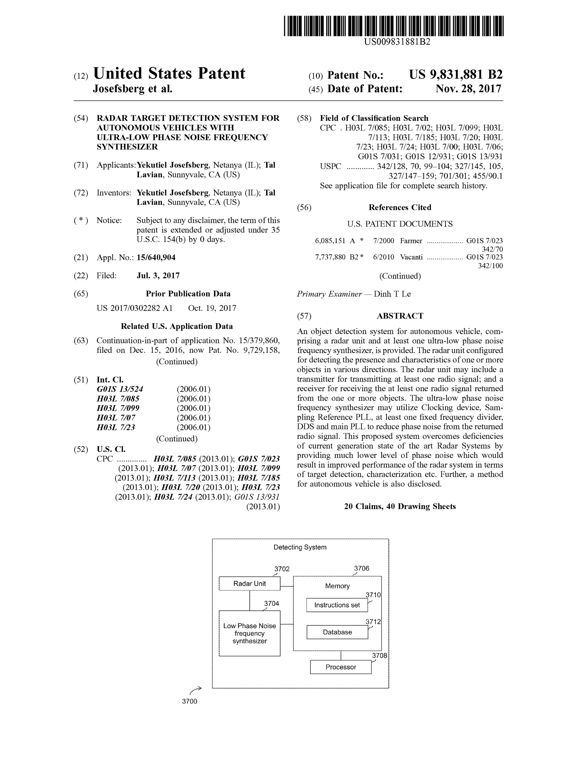
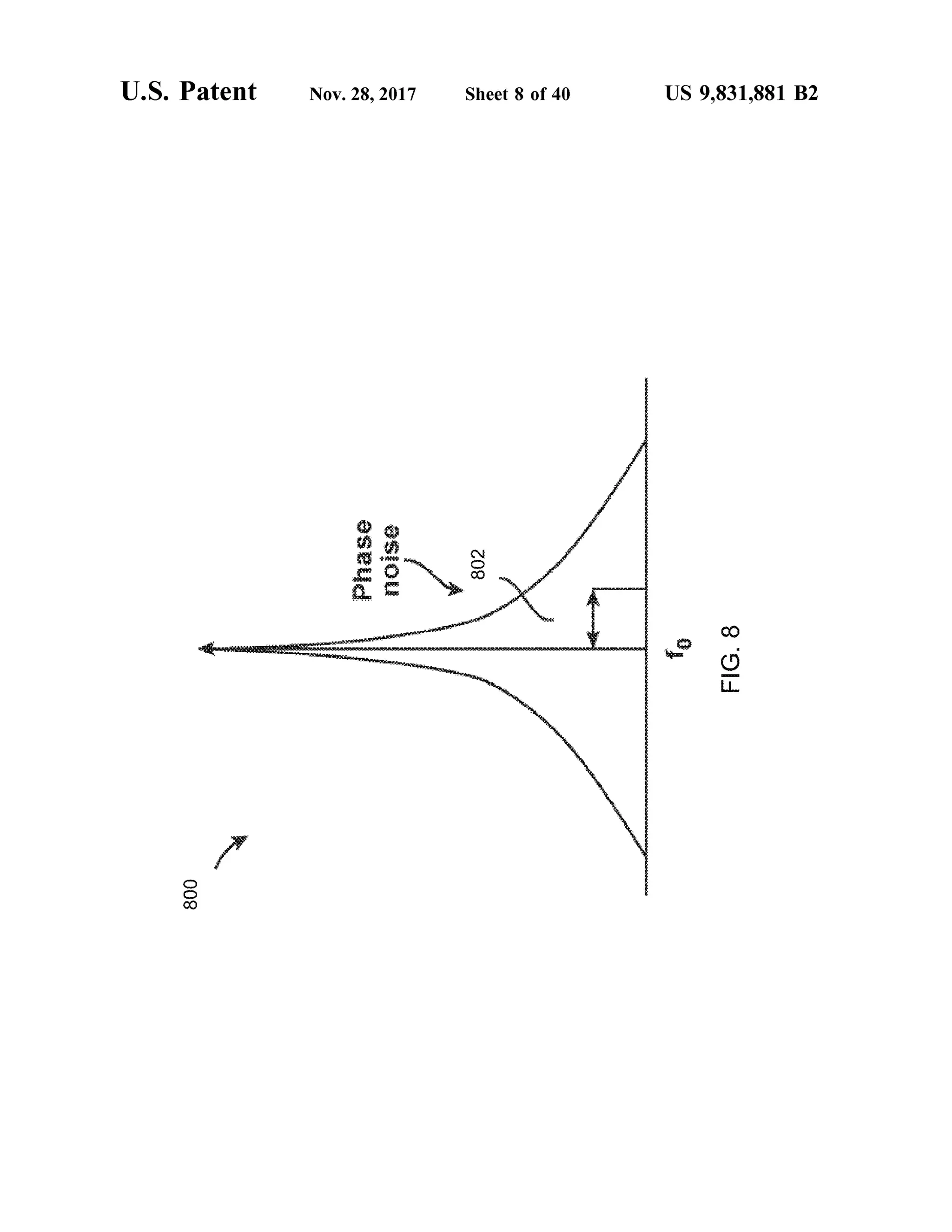
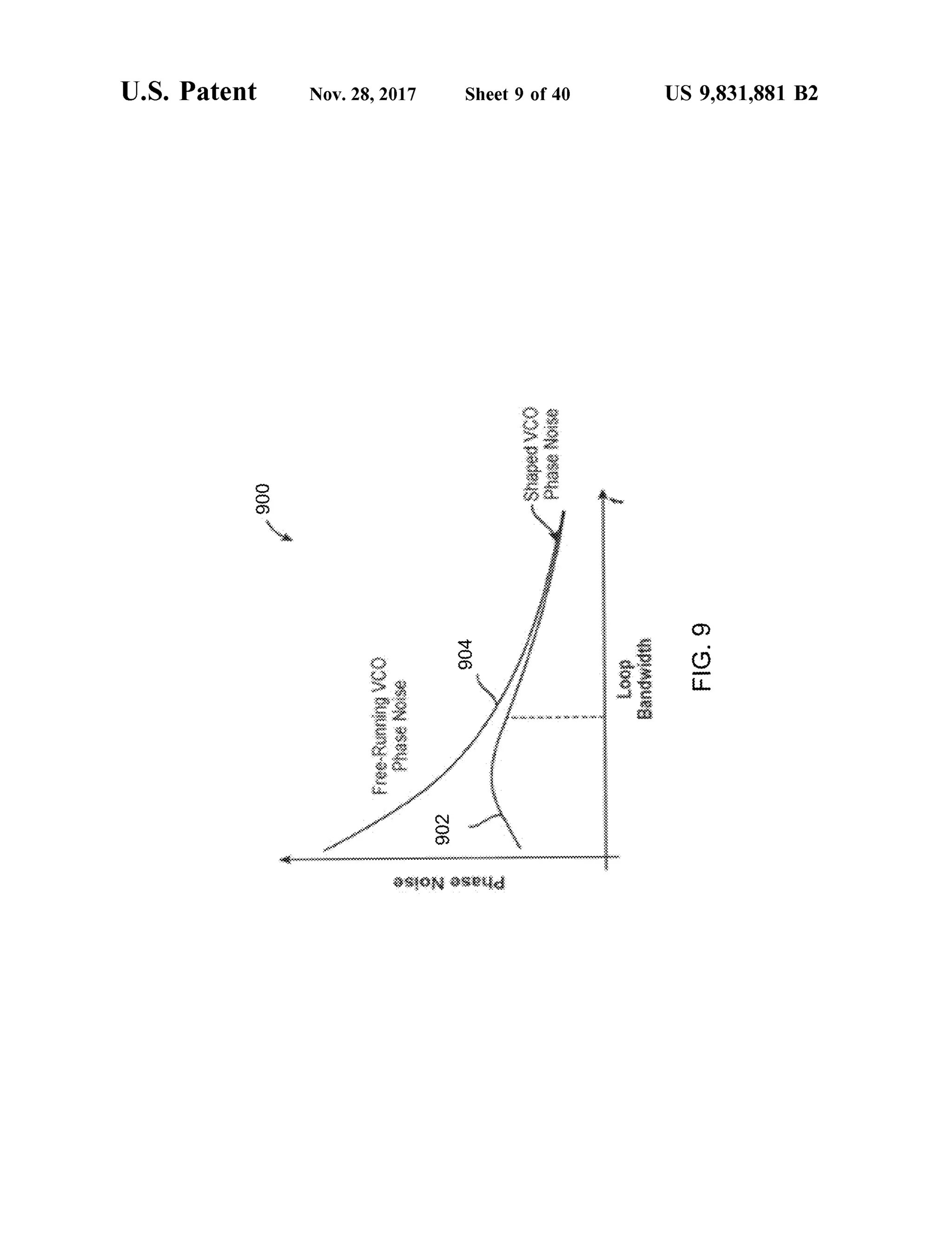
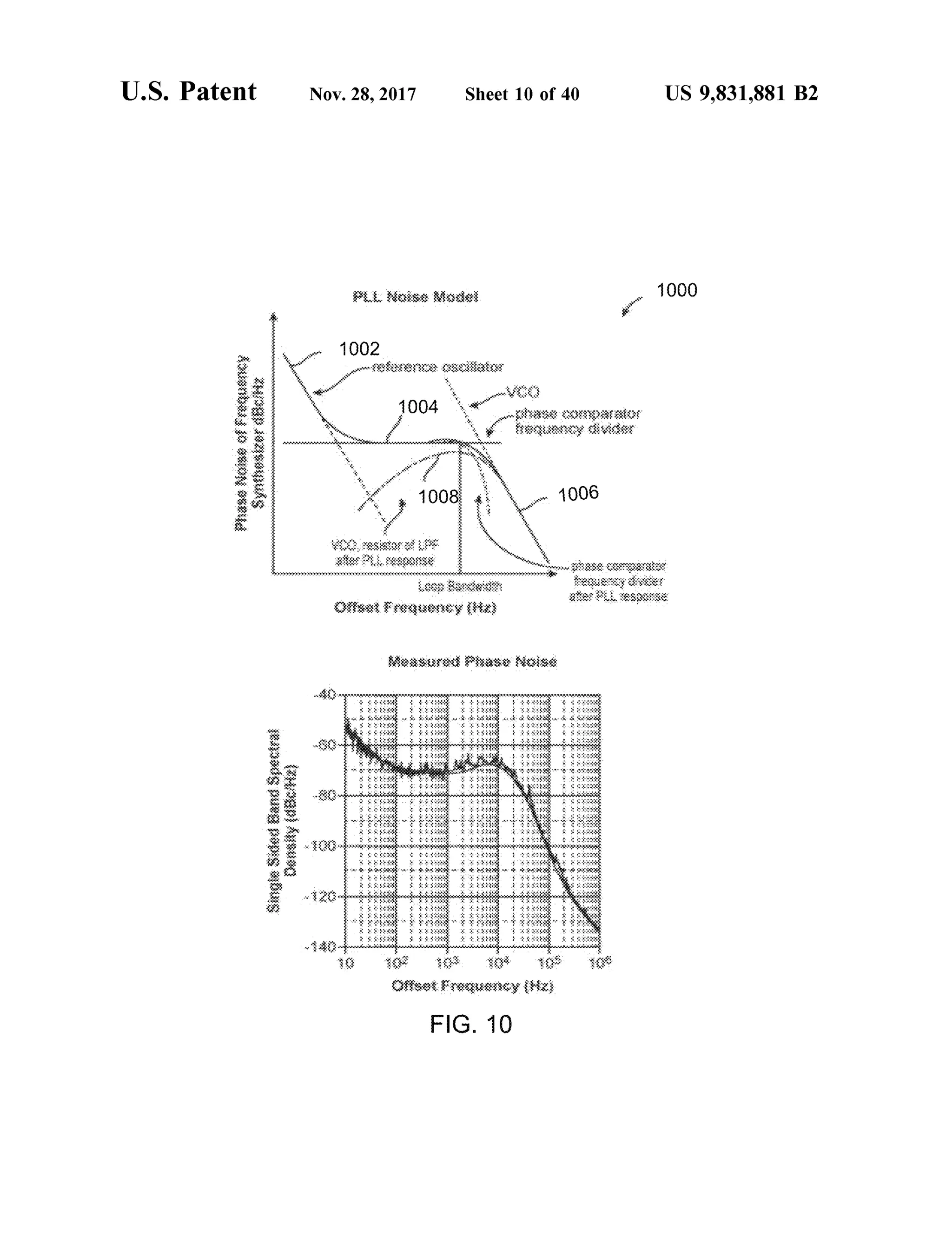
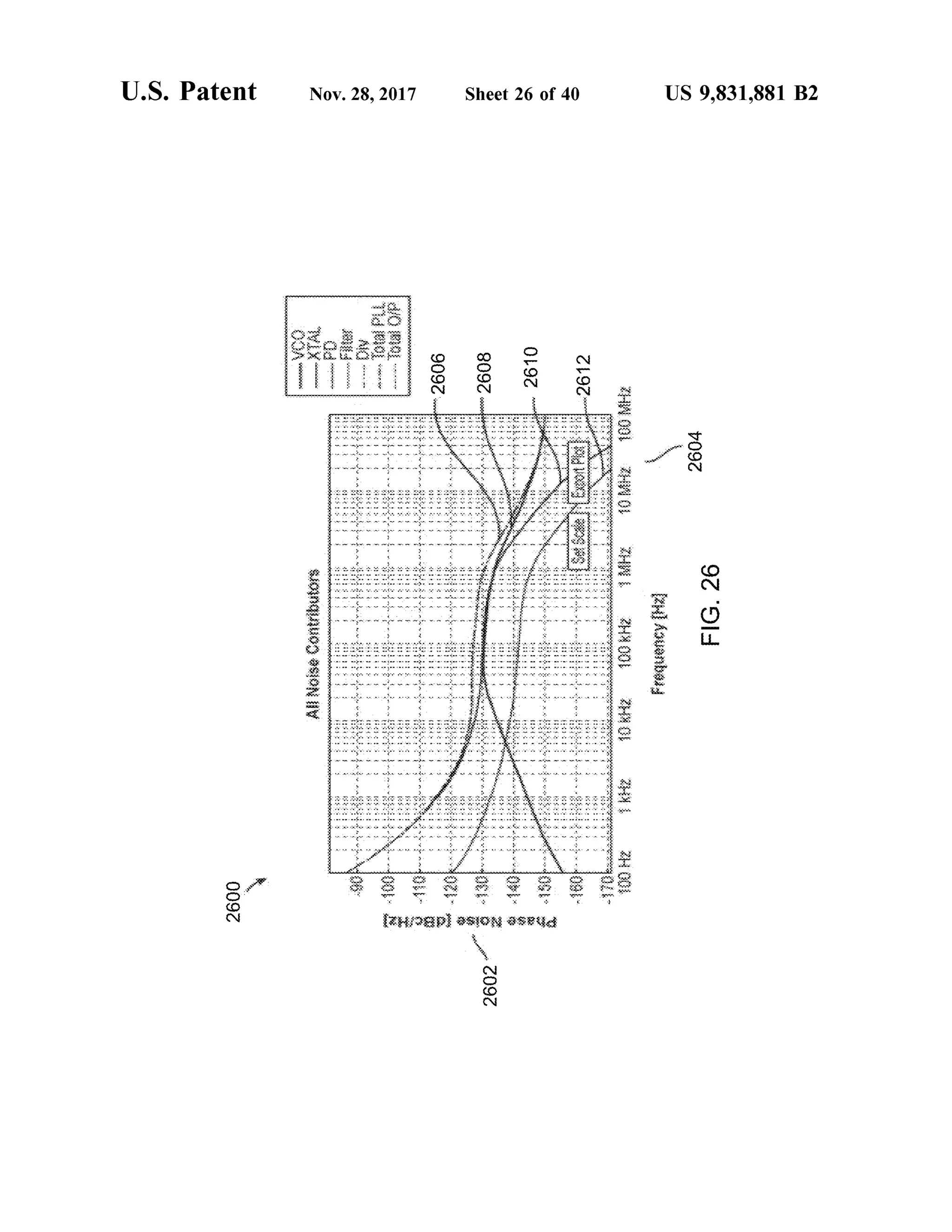
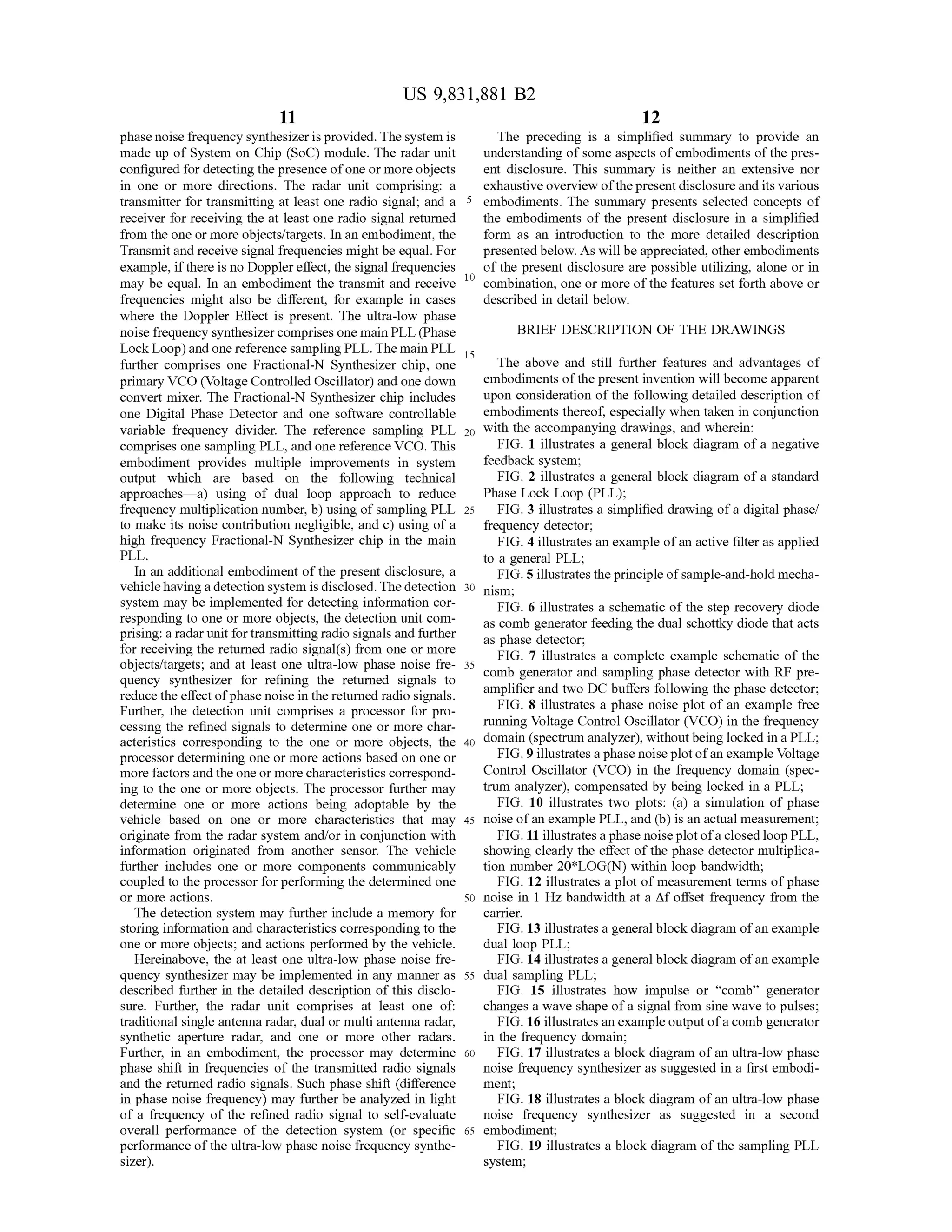
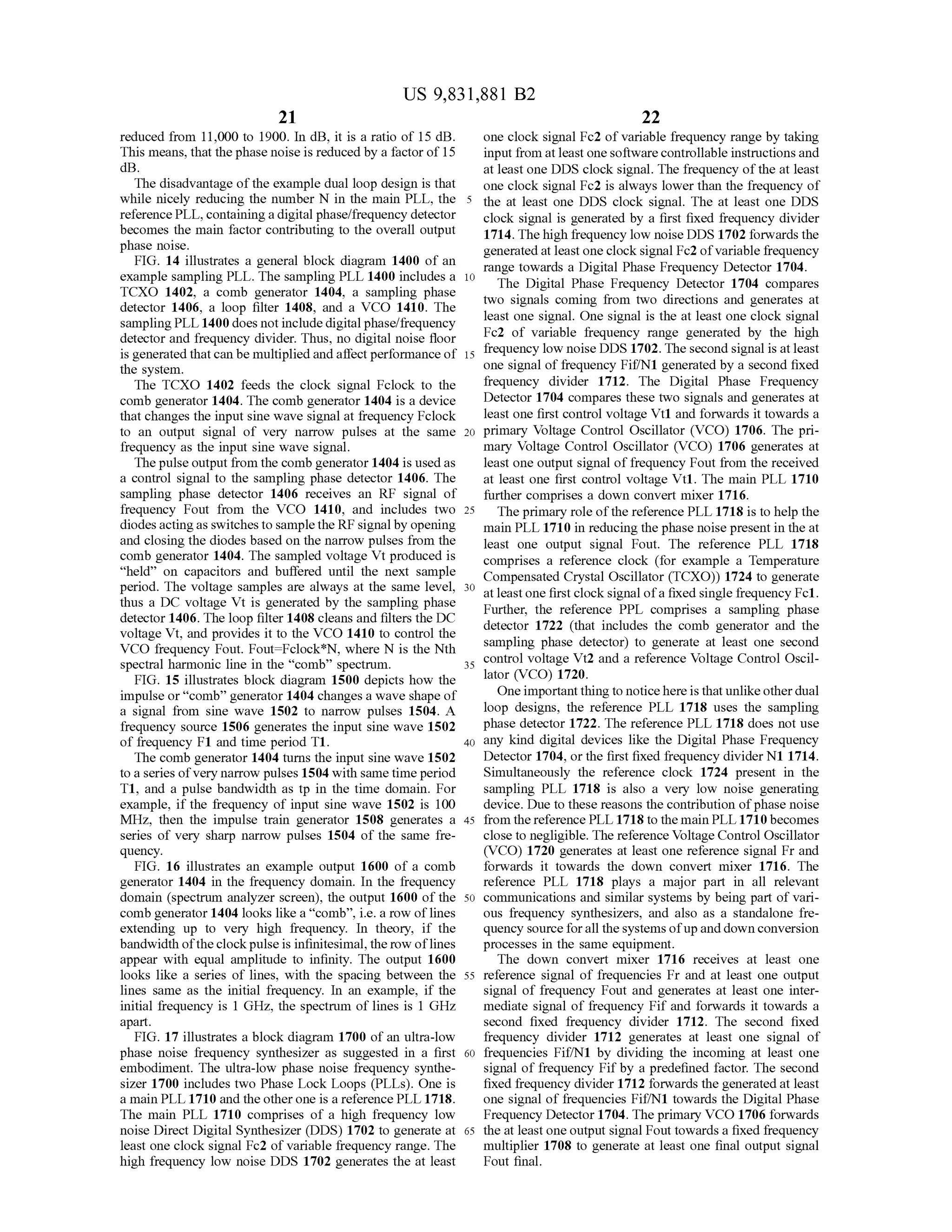
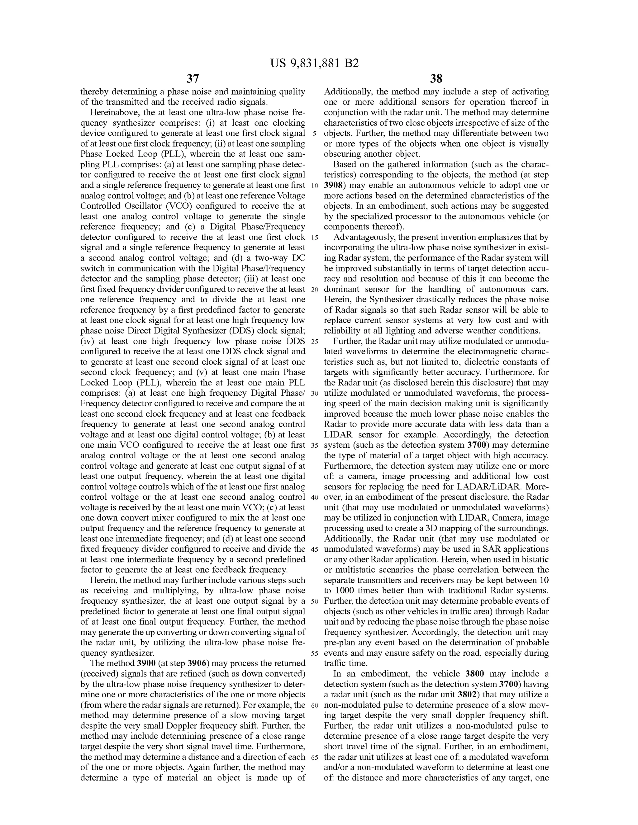
noise of an example PLL. The simulation graph showsthe noise from one offset frequency to another one. Following
overall phase noise of the example PLL and includes the are four different equations and terms to define integrated
contribution of all the components that contribute to the phase noise:
phase noise. The simulation graph illustrates first, second
and third regions 1002, 1004 and 1006 of the phase noise. 5
The first region 1002 which is very close to the carrier
depicts a steep line which basically comes from the refer
ence clock such as the Temperature Controlled Crystal
Oscillator (TCXO ,or any other reference clock device). The
firstregion depicts thenoise ofthe TCXO ,multipliedby 20
log N ,where N is the ratio of output frequency to the clock
frequency. The second region 1004 depicts a flatphase noise
which isbasically thenoise floorofthe digitalphase detector
multiplied by thesame ratio of 20 log N . The third region 15
1006 depicts a steep line which is the inherent VCO phase Where the first equation describes single sideband phase
noise not affected by the loop bandwidth and locking phe noise [dBc]
nomenon. The dashed line 1008 depicts the VCO “cor- The 2nd equation describes the spectral density of phase
rected” phase noise inside loop bandwidth . Below the flat modulation, also known as RMS phase error (degrees)
area, the compensated VCO phase noise doesnotaffect the 20 The 3rd equation describes the spectraldensity offrequency
overall result because it is way below the noise floorof the fluctuations,also knownasRMS frequency error orresidual
phase detectormultiplied by that ratio. The actualmeasure- FM (Hz)
mentof phase noise ofan example PLL is illustrated in FIG . The 4th equation describes the spectral density of fractional
10 (b). One can see clearly the similarity between the two
curves. 25 For example, the firstequation defines the PhaseNoise in
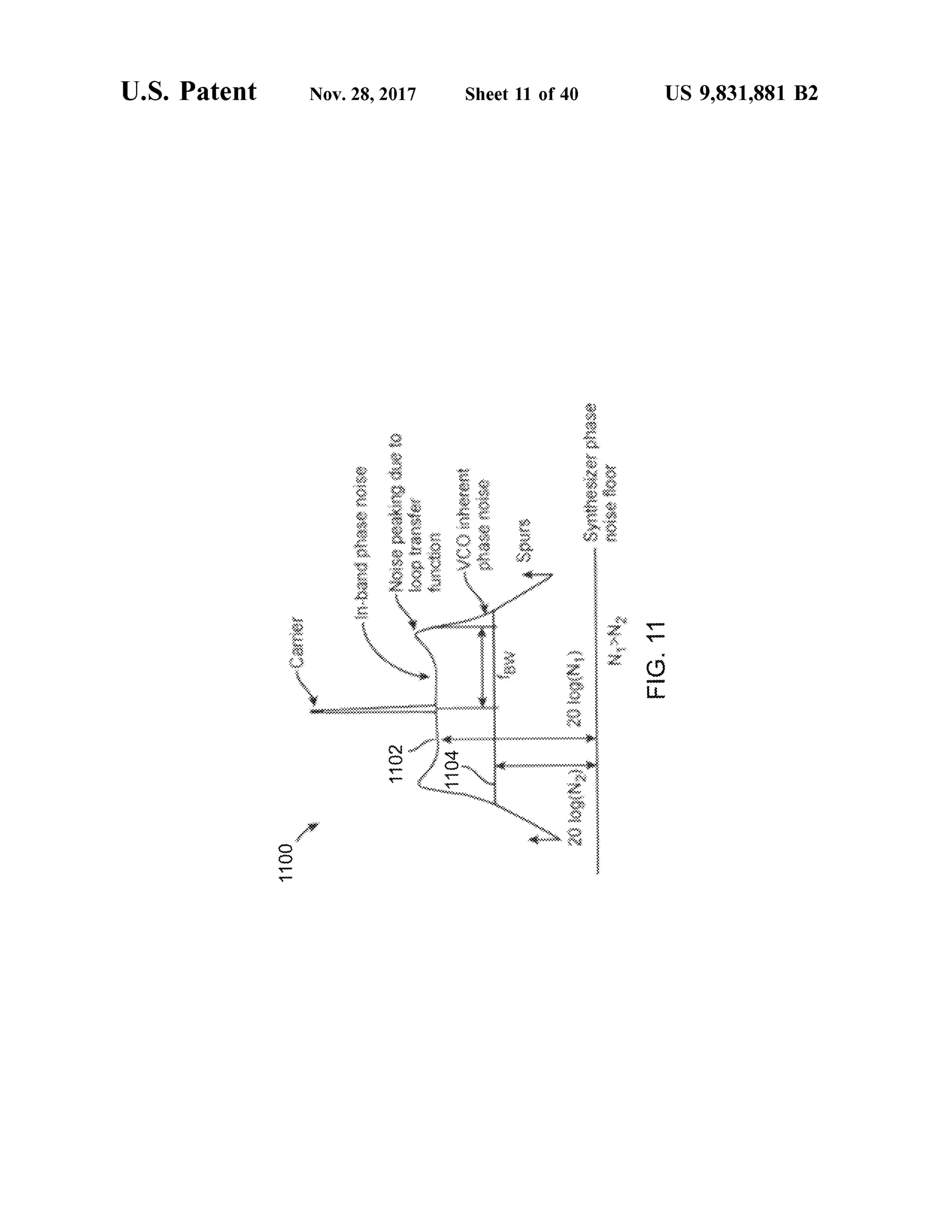
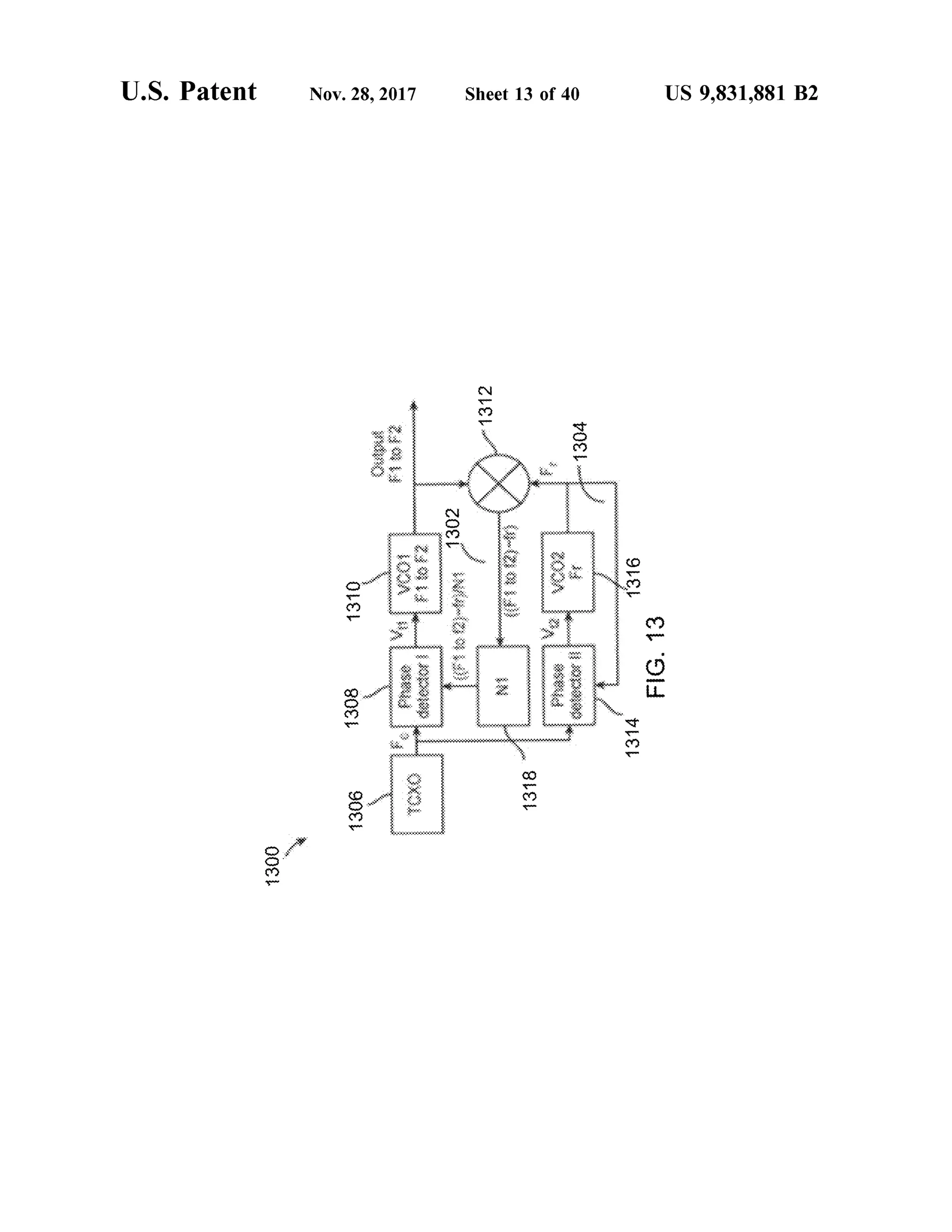
FIG . 10 illustratesa phase noiseplot1100ofa closed loop dBc. It can be translated by the 2nd equation to degrees
PLL , showing clearly the effect of the phase detector mul (relevant in respectoflearningmodulation schemes). Asper
tiplication number 20*LOG (N )within loopbandwidth . The further equations,the phase noise can also be translated inphase noise plot800 illustratesphase noiseson both sides of termsof Hz and timedomain phase jitter seconds.the carrier frequency fo,where the left side is a mirrored 30 FIG . 13 illustrates a general block diagram 1300 of animage of the rightside. The phase noises on both sides ofthe example dual loop PLL . The main target of the dual loopcarrier fo looks like it is passing through a band-pass filter. design is to reduce themultiplication number N in themainAs illustrated , on both sides, the in -band phase noise
PLL.inside the loop bandwidth is flat in shape and is equal to the
phase detectorand/orthe referenceclock noisemultiplied by 35 The dual loop PLL 1300 includes an upper PLL 1302,
20 log N . Atthepoint of the loop bandwidth , thephase noise referred to as a main PLL 1302, and a lower PLL 1304,
goes up before going down again. This is due to addition of referred to as a referencePLL 1304,a TCXO 1306 operating
3 dB due to a combination ofphase noiseofthe free running as a master clock, feeding a clock signal Fc to both the
VCO and the phase detector. The upper straightline 1102 primary PLL 1302 and the reference PLL 1304.
depictsa phase noise contributed by the phase detector atN1 40 The reference PLL 1304 includes a first phase detector
and the lower straight line 1104 depicts a phase noise 1314,and a single frequency first VCO 1316 thatoperatesat
contributed by thephase detector at N2. It can be seen that, a reference frequency Fr. The reference frequency Fris fed to
there is difference in phase noise in the flat area, due to two a first input of a down convertmixer 1312.
different “ N ” numbers. The phase detector contributes a The main PLL 1302 includes a second phase detector
higher in-band phase noise at a higher value of N . 45 1308 and a second VCO 1310 that generates an output
Thus, in order to achieve low phase noise, it is essential frequency range F1to F2. A sample ofthe output frequency
to: a ) choose components such as phase detector and refer range F1to F2 is fed to thesecond inputofthe down convert
ence clock with the lowest inherent phase noise possible, mixer 1312 andmixed with a single reference frequency Fr.and b ) lower the ratio number N asmuch as possible. The output from the down convertmixer 1312 is at a much
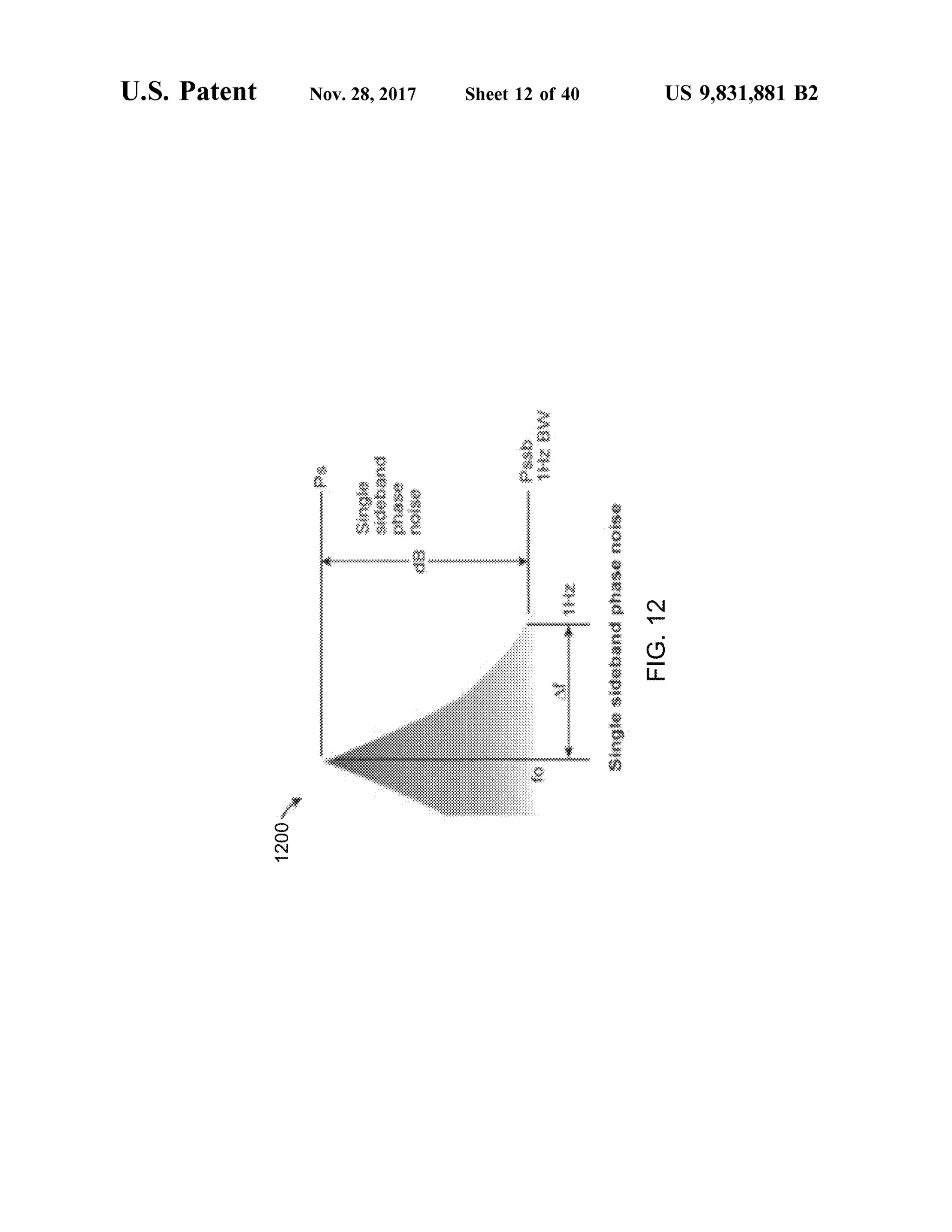
FIG . 11 illustrates plot 12902200 ofmeasurement terms 50 10lower frequency (F1 to F2)-Fr. This lowered frequency isof phase noise in 1 Hzbandwidth at a Afoffset frequency fed back to the second phase detector 1308 through afrom the carrier. The phase noise expression is usually in
frequency divider 1318 of value N1.dBc, i.e. dB relative to the carrier c power levelPs, in other
words how low it is compared to the carrier per Hz, in a Therefore: a )Withoutthe down convertmixer 1412: F1to
bandwidth of 1Hz. That is basically theterm thatisused for 55 F5 F2= NxFc, b ) With the down convert mixer 1312: (F1 to
phase noise,dBc per Hertz (dBc/Hz) ata certain Affrom the F2)-Fr=N1xFc. As a result there is a reduction in the
carrier. number N : N1/N = ((F1 to F2) - Fr)/ (F1 to F2).
Asan example for themeasurementmethod, suppose AF The N1 number is basically the division number that the
is 10 KHz, the phase noise power level Pss is measured at frequency divider 1318 will use to divide the outputof the
the level of -70 dBm on the spectrum analyzer, and the 60 mixer 1312 and feed to the second phasedetector 1308. The
carrier power level Ps is measured at the level of 10 dBm , value ofN1 is set as minimal, as the output from the mixer
the ratio between the Ps 10 dBm and the PssB -70 dBm at 1312 is ata much lower frequency than original frequency
10 KHz from the carrier is therefore 80 dB , so the phase range F1 to F2.
noise at 10 KHz offset from carrier and is - 80 dBc/Hz. To give an example: a ) Suppose Fc= 1 MHz, b ) Suppose
Formany systems, the important parameter to evaluate 65 F1to F2= 10,000 to 11,000 MHz. Then N = 10,000 to 11,000.
performance is not the phase noise measured at a single Now If Fr= 9000 MHz, then ((F1 -F2)- Fr)= 1000 to 1900
frequency offset from the carrier, but the integrated phase MHz. Then N1=1000 to 1900. Thus, the value of N is](https://image.slidesharecdn.com/us9831881-200618140046/75/Radar-target-detection-system-for-autonomous-vehicles-with-ultra-low-phase-noise-frequency-synthesizer-52-2048.jpg)

The document is a United States patent (US 9,831,881 B2) granted on November 28, 2017, for a radar target detection system designed for autonomous vehicles that incorporates an ultra-low phase noise frequency synthesizer. The invention aims to enhance object detection capabilities by significantly reducing phase noise in radar signals, thereby improving the performance of the radar system. The application also includes details about inventors, related application data, and the classification of the technology.