Download to read offline
![FIG.7
US 2017/0302282A1
inminingunaformaammo
m
ongmove
danwarnamerawat
a
Oct.19,2017 Sheet 7 of 40
VINAWA
may
Awan
n a
WAX
E.AV.AVA.AV
has-***
*****
Mitmiste
vero
non
Permanamente
costantede pregatitng mahig
Patent Application Publication
D}]
[b
]](https://image.slidesharecdn.com/us20170302282a1-200617153345/75/Radar-target-detection-system-for-autonomous-vehicles-with-ultra-low-phase-noise-frequency-synthesizer-8-2048.jpg)
![Patent ApplicationPublication Oct.19,2017 Sheet 14 of 40 US 2017/0302282Al
1410 ·
|1408
1406
???
FIG.14
14021404?” ]1400](https://image.slidesharecdn.com/us20170302282a1-200617153345/75/Radar-target-detection-system-for-autonomous-vehicles-with-ultra-low-phase-noise-frequency-synthesizer-15-2048.jpg)
![0:(
Cols?
}€?kiraf?243
?
'ff
?
!''*
????
??-
f
"
FHI
]!}flyfV7
/#
?
?
?
??
???
????
?????
??????
?:?..'.?..??:_'
??????????????
????????
??:,?????????????
??.??
???????.?.:-????
?
?
??????????????????????????????????????????????..??????????????????...?????????......???????????????????????.
?.????????????4?????????????????..;.??:;
£
?
P£££
?
-?-??..--?
Oct.19,2017 Sheet 21 of40 _ US2017/0302282 Al
?
?..??
???????
????:;?!?
?:*;*-???????
??:?????????
?
??
/tt?
???
?
??
???::;???
??
????-*??-??????.:??
?.:???????
?...;:.????;".'..??:
??????
??????
????????
.????????
??????_;.???????
?.????????..
????..?-??
?????.???????
??????????
????
???????????3:_
?
?LL?017.ni
C010
?
????!? xesmeis&fac
?? 3
??????
? ? ? ?? ?
???????
?
-C&80
??
?????_
??..?.:???
????????
???
°:?????????;.-???????.?
??ii:???????
??????:4.,??????.???
|??
:;?
?
?
???
??
??
?
???#?
.????
?.??
90&C
???
????4???
?
q.
?
:?????????????????????
?.?..?.:.:???'
?
??
??????????
???????'.',??
'??????????????:*??.????
????????????????..???.'.??????
Arcx--??????*?'1
qv'???????;$
.??????????????????????????
.
?
???
?
?
.????
????
??????
?.?.;fi?
??
?.
.;.????..
'.:'.??|.??
.
...???
??
? . .
???????????
?
??
??????
????.
??:?
??
??:(dk?????.?
????
??????????????????? ?
?
?
??
??????????????????????????
? ?
.;?????
???????
?.
???
?
??
?
.????????.?_
??????????????
????????
????????????
??
;:;??;:.???.?????????????..
???????.....???????????????
??????????????????
???????????????
?
???
?
??
'£
?
fi{Y
848029%
28!?%8683f3?
00PM
Patent Application Publication](https://image.slidesharecdn.com/us20170302282a1-200617153345/75/Radar-target-detection-system-for-autonomous-vehicles-with-ultra-low-phase-noise-frequency-synthesizer-22-2048.jpg)
![y07
Cola
IHUApuanbass
?
?
?
?
?
??{
{
RI
{{
{{
{
{
{
{
HI
{
??????????????????????????????????????
??????????????????????????????????????
????????????????????????????}}?."?'.:????-:.:?.????
??????????..????????????????????????
?
????????.???????????
??????????????????????????????
?
???????.
?
????????
?:??||??.
????
Oct.19,2017 Sheet 24 of40 _ US2017/0302282 Al
?
$??
?
.*.?...?-?.
????
???
?
?
.
?
????:.
. . . . . . . . . .. . . : '
:??????????
???.????????.
??????4??
,..??????.".
???:;?!..??.?.4????????
???????-:????4
?????????????????????..?
??
??010
-.-.??
..
-:-????
-..
?
?
?????
?
???????
?
?
?
80Z
. .
.
?xf..?
??????
?????????????????????????????????
?????::'..??????????
??????
?????:_
??????????????????????????
Z0Z
??||?
???
?
?
????????
??????
?
.
?
??
?
..-:?
??????
--.?.????.???
??
???
?Z'90
?
PhaseNoise(dBc/H2)
???????????????
?
??
????
??????????
???
3 .
?
??????????
?.????????????????
??????..?????????..?;.??.??'??°.
??????????????????????
?????..?.:?.?????????????.????
????
??
?
?
????
.?
??
?????
8:
3%83?
?
3
??
?
?
?
??
???
?..??????????????????????:?."?.;.;??"
?????????????
??????
.:.??????.?.'?.???????????.??.??1??
??:?.???????????::::'.?.???????.???????.?
???????????????????????????????????..
;:????????????????????
?????????&??.
??????'.:???????????????????.;?!!.??????????????????????????..
??????????????
3
??????????
'?sP??????????!XI?]32.
Patent Application Publication
_00Z](https://image.slidesharecdn.com/us20170302282a1-200617153345/75/Radar-target-detection-system-for-autonomous-vehicles-with-ultra-low-phase-noise-frequency-synthesizer-25-2048.jpg)

![US 2017/0302282 A1 Oct.19,2017
RADAR TARGET DETECTION SYSTEM FOR
AUTONOMOUS VEHICLES WITH
ULTRA-LOW PHASE NOISE FREQUENCY
SYNTHESIZER
CROSS-REFERENCE TO RELATED
APPLICATIONS
[0001] This application is a continuation-in-part of U.S.
application Ser.No. 15/379,860 filed on Dec. 15, 2016, is a
continuation ofU .S.application Ser.No.15/229,915 filed on
Aug. 5, 2016, now U .S. Pat. No. 9,705,511, which claims
priority to U .S. ProvisionalPatent Application No.62/181,
221 filed on Jun. 18, 2015,the disclosure ofwhich ishereby
incorporated by reference in its entirety.
[0002] This patent application relates to the following
co-assigned applications that are each incorporated by ref
erence:
[0003] International Patent Application number PCT/
M2016/054790 filed on Aug. 9 , 2016. U .S . Pat. No. 9,660,
655 granted May 23, 2017, based on U .S. application Ser.
No. 15/379,915 filed on Dec. 15, 2016.
FIELD
[0004] Embodiments of the present disclosure are gener
ally related to sensors for autonomous vehicles (for
example,Self-Driving Cars)and in particularto systemsthat
provide ultra-low phase noise frequency generation for
Radar Application for autonomous vehicles.
Sensor Technologies:
[0012] Simple cars and other types ofvehicles are oper
ated byhumansand thesehumansrely on their senses such
as sightand sound to understand their environment and use
their cognitive capabilities to make decisions according to
these inputs. For autonomous cars and other autonomous
vehicles, the human sensesmustbe replaced with electronic
sensors and the cognitive capabilitiesby electronic comput
ing power. The most common sensor technologies are as
follows:
[0013] LIDAR (LightDetection andRanging) — is atech
nology thatmeasuresdistance by illuminating its surround
ings with laser lightand receiving the reflections.However,
the maximum power of the laser light needs to be kept
limited to make them safe for eyes, as the laser light can
easily be absorbed by eyes. Such LIDAR systems are
usually quite large, expensive and do notblend in well with
the overall design of a car/vehicle. The weight of such
systemscan be as high as tensofkilogramsand the cost can
be expensive and in some cases high up to $100,000.
[0014] Radar (Radio Detection and Ranging) — These
days Radar systems can be found as a single chip solution
that is lightweight and cost effective. These systemswork
very well regardless of lighting or weather conditions and
have satisfying accuracy in determiningthe speedofobjects
around the vehicle.Having said the above, mainly because
of phase uncertainties the resolution of Radar systems is
usually notsufficient.
[0015] Ultrasonic sensors— These sensors use sound
waves and measure their reflections from objects surround
ing thevehicle. These sensors are very accurate andwork in
every type oflighting conditions.Ultrasonic sensorsare also
small and cheap and work well in almost any kind of
weather,butthatisbecause of their very short rangeofa few
meters.
[0016] Passivevisualsensing — This type ofsensing uses
cameras and image recognition algorithms. This sensor
technology has one advantage that none of the previous
sensortechnologieshave colour and contrastrecognition. As
with any camera based systems, the performance ofthese
systems degrades with bad lighting or adverse weather
conditions.
[0017] The table below is designed to provide a better
understanding of the advantages and disadvantages of the
different current sensor technologies and their overall con
tribution to an autonomous vehicle:
[0018] The following tablesscores thedifferent sensors on
a scale of 1 to 3,where 3 is the best score:
BACKGROUND
Autonomous Cars:
Levels of Autonomous Cars:
100051 According to the Society of Automotive Engineers
(SAE) cars and vehicles in general are classified into 5
different classifications:
[0006] Level 0: Automated system has no vehicle con
trol,butmay issuewarnings.
[0007] Level 1: Drivermustbe ready to take control at
any time. Automated system may include features such
as Adaptive Cruise Control (ACC), Parking Assistance
with automated steering,and Lane Keeping Assistance
(LKA) Type II in any combination.
[0008] Level 2: The driver is obliged to detect objects
and eventsand respond if the automated system fails to
respond properly. The automated system executes
accelerating, braking, and steering. The automated sys
tem can deactivate immediately upon takeoverby the
driver.
[0009] Level 3: Within known, limited environments
(such as freeways), the driver can safely turn their
attention away from driving tasks, but must still be
prepared to take controlwhen needed.
[0010] Level 4 : The automated system can control the
vehicle in all but a few environments such as severe
weather. The drivermust enable the automated system
only when it is safe to do so. When enabled, driver
attention is not required.
[0011] Level 5:Other than setting the destination and
starting the system ,no human intervention is required.
The automatic system can drive to any location where
it is legal to drive and make its own decisions.
Item LIDAR RADAR Ultrasonic Camera
Proximity Detection
Range
Resolution
Operation in darkness
Operation in light
Operation in adverse Weather
Identifies colour or contrast
Speed measurement
ANNWWNNE wwwwwwANN
wwwwww ????????????????????|
Size
Cost
Total 18 24 22 21](https://image.slidesharecdn.com/us20170302282a1-200617153345/75/Radar-target-detection-system-for-autonomous-vehicles-with-ultra-low-phase-noise-frequency-synthesizer-42-2048.jpg)
![US 2017/0302282 A1 Oct. 19, 2017
[0019] The above presentation of the state of the tech-
nology proved a high-levelview of the advantages and
disadvantages of the technologies from differentper
spectives.
Drawbacks of Current Sensors:
[0020] As shown in the table above,the available sensors
for existing autonomousvehicles areLIDAR , Sonar,passive
vision (cameras), and radar.Many of these sensors come
with significant drawbacks, while radar systems do not
experience most of the drawbacks and thus better among
other sensors, based on the table shown above:
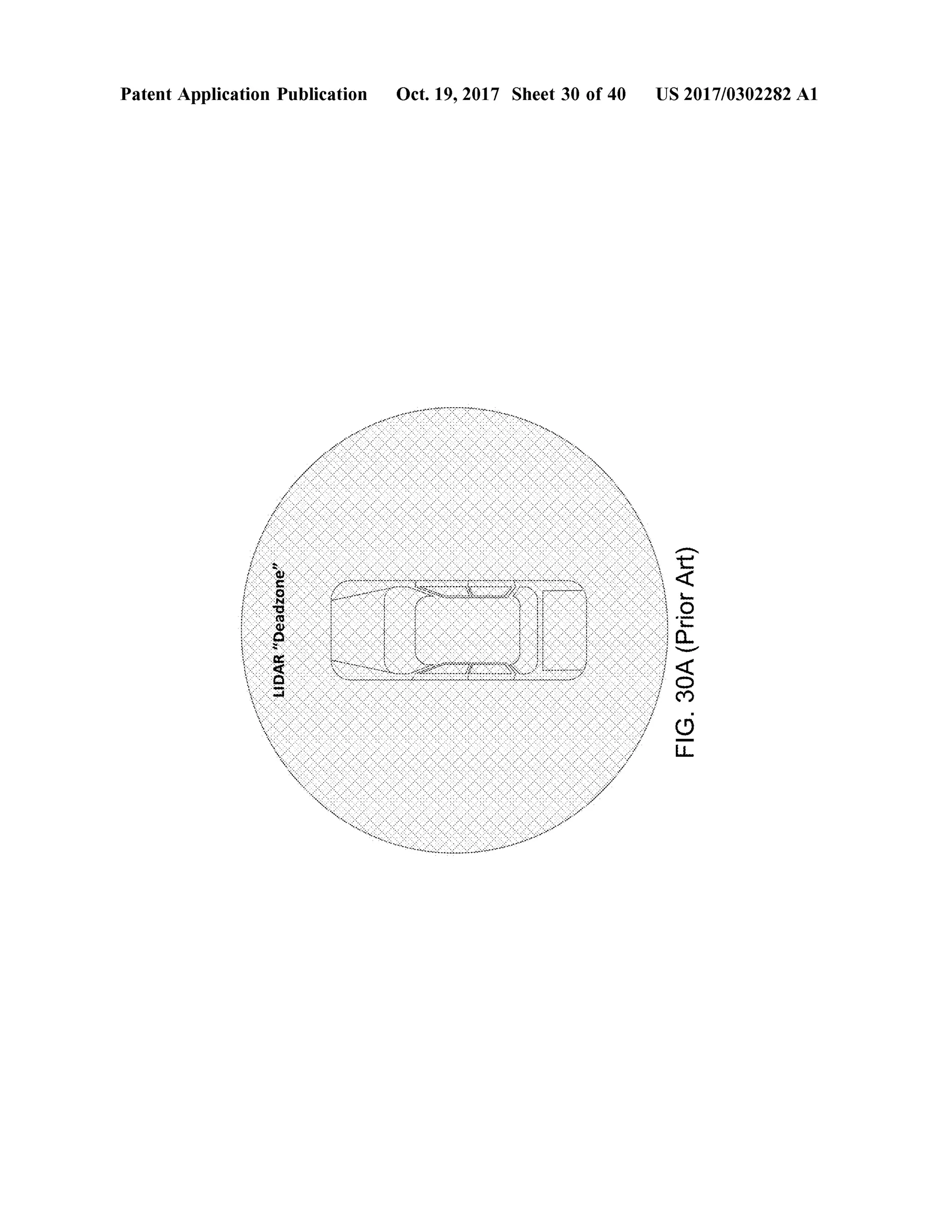
[0021] For example, LIDAR systemshave a " dead zone”
in their immediate surroundings (as shown in FIG . 30A ),
while a Radar system will be able to cover the immediate
surroundings of a vehicle as well as long range with
enhanced accuracy.
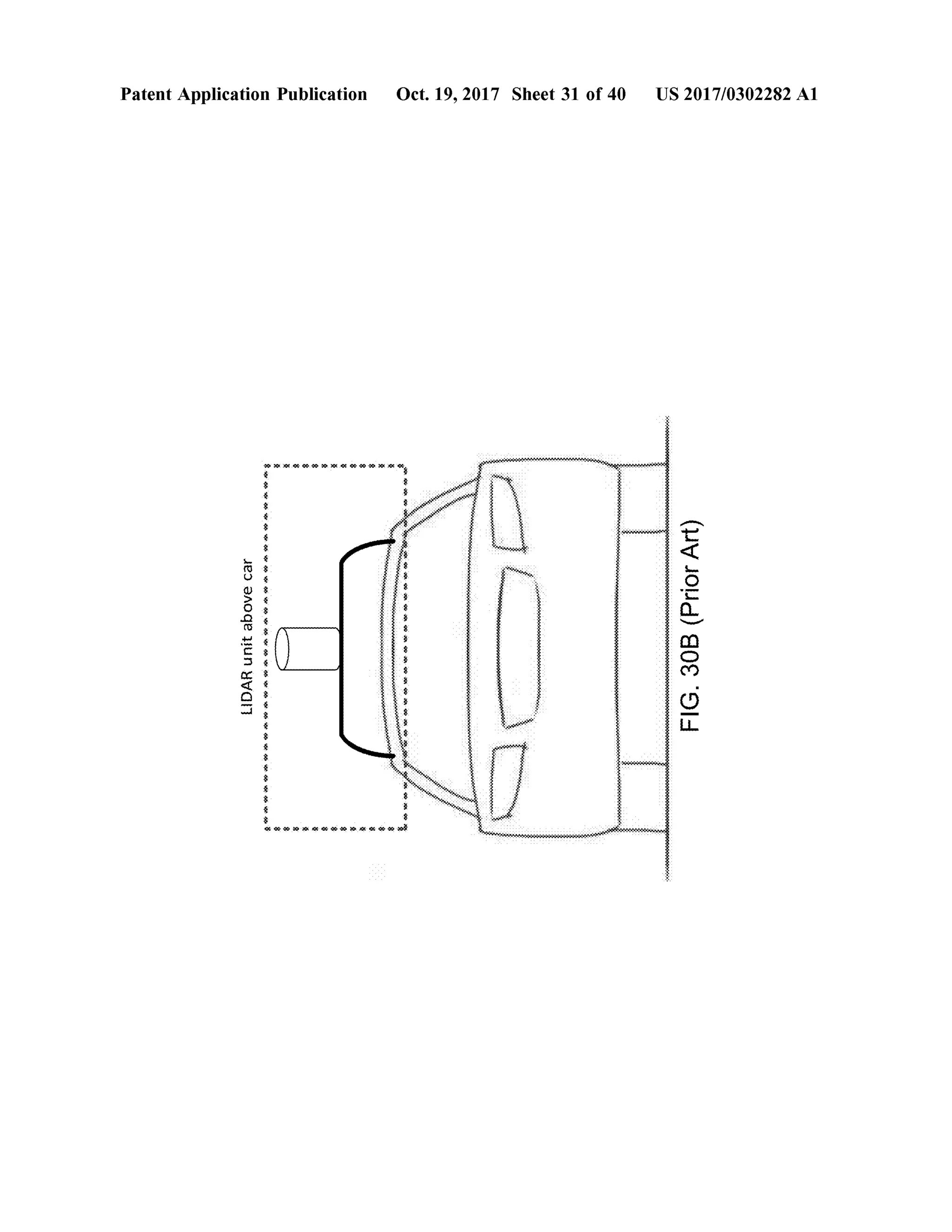
[0022] In orderto eliminate the “dead zone” asmuch as
possible LIDARs are mounted tall above the vehicle (as
shown in FIG . 30B ). These limits the options of using
parking garages, causes difficulty in the use of roof top
accessories and finally also makes the vehicle less market
able since such a tower does not blend in well with the
design of a vehicle.
[0023] Typical LIDAR systems generate enormous
amounts of data which require expensive and complicated
computation capabilities,while Radar systemsgenerate only
a fraction of this data and reduce the cost and complication
ofon board computation systemssignificantly.For example,
some types ofLIDAR systemsgenerate amounts of 1 -Gb/s
data that require substantial amount of computation by
strong computers to process such high mount of data. In
some cases, these massive computations require additional
computation and correlation of information from other sen
sors and sources of information. In some cases, the source
for additional computations is based on detailed road infor
mation collected over time in databases or in enhanced
maps. Computations and correlations can be performed
against past information and data collected over time.
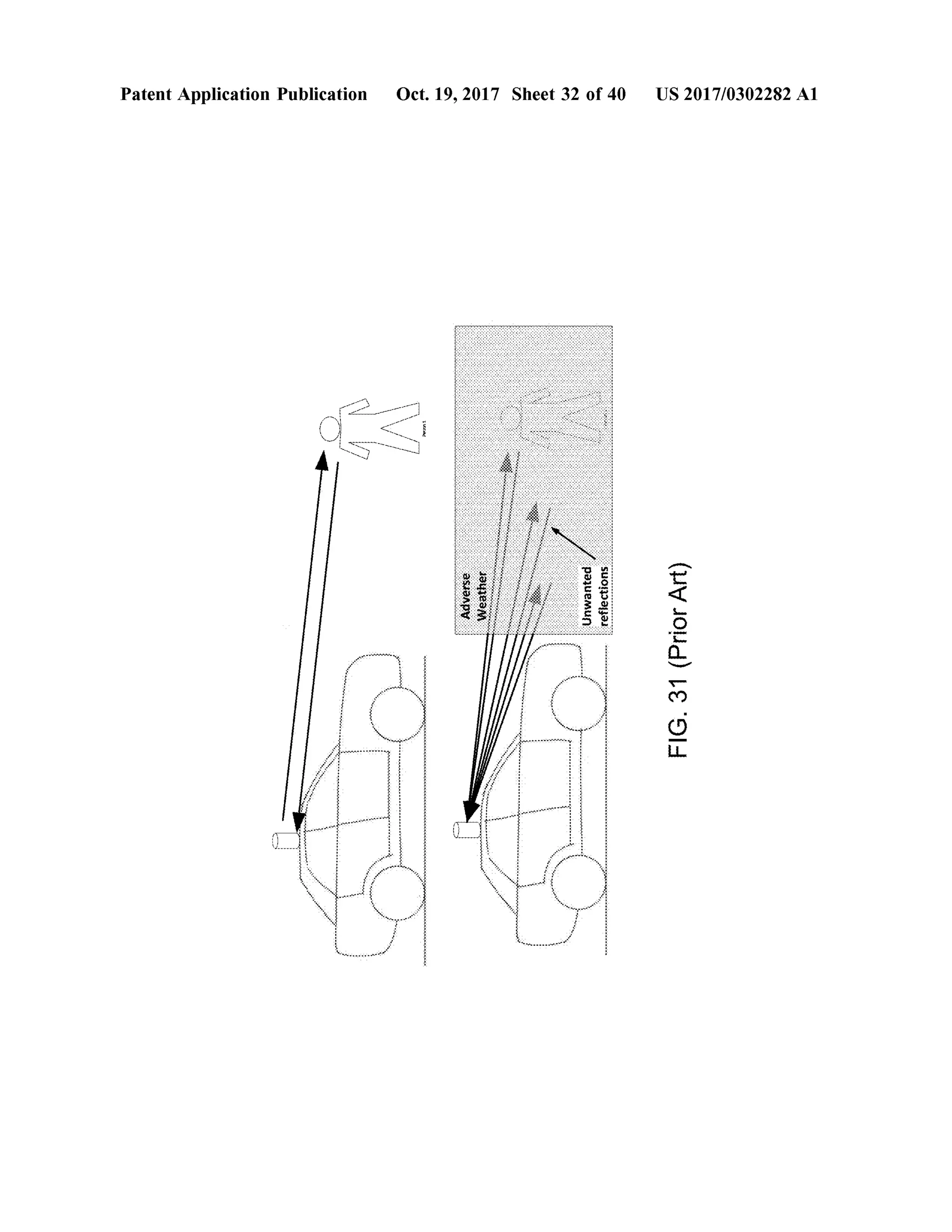
[0024] Typical LIDAR systems are sensitive to adverse
weather such as rain, fog and snow while Radar sensors are
not. A radar system will stay reliable and accurate in adverse
weather conditions (as shown in FIG . 31). LIDAR systems
use mechanical rotation mechanisms that are prone to fail
ure, Radars are solid state and do nothavemoving parts and
as such have a minimal rate of failures.
[0025] TypicalLIDAR systemsrely on a rotation speed of
around 5-15 Hz. This means that if a vehicle moves at a
speed of65 mph, the distance the vehicle travels between
"looks” is about 10 ft. Radar sensor systems are able to
continuously scan their surroundings especially when these
systems use one transmitting and one receiving antenna
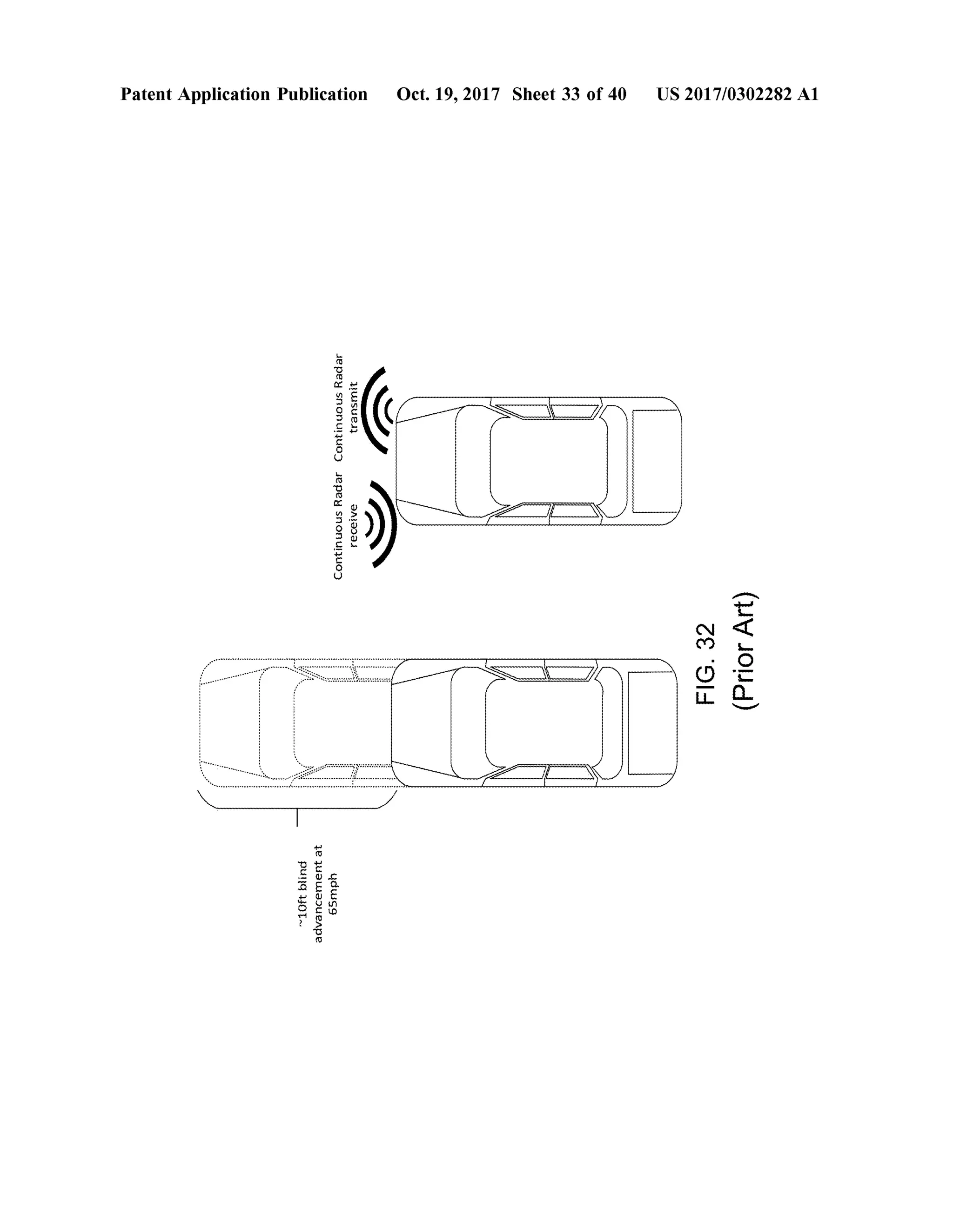
(Bistatic system ) (as depicted in FIG . 32). Further,LIDAR
systemsare not accurate in determining speed and autono
mous vehicles rely on Radar for accurate speed detection.
0026 ] Sonar: Sonar sensors are very accurate, but can
cover only the immediate surroundings of a vehicle, their
range is limited to severalmeters only. The Radar system
disclosed in this patent is capable ofcovering these imme
diate surroundings as well and with similar accuracy. Fur
ther, Sonar sensors cannot be hidden behind cars' plastic
parts which poses a design problem , Radars can easily be
hidden behind these parts without being noticed.
(0027] Passive Visual sensing (Cameras): Passive visual
sensing uses the available light to determine the surround
ings of an autonomous vehicle. In poor lighting condition
theperformance of passive visualsensing systemsdegrades
significantly and is many times depending on the light that
the vehicle itself provides and as such does notprovide any
benefit over the human eye. Radar systems, on the other
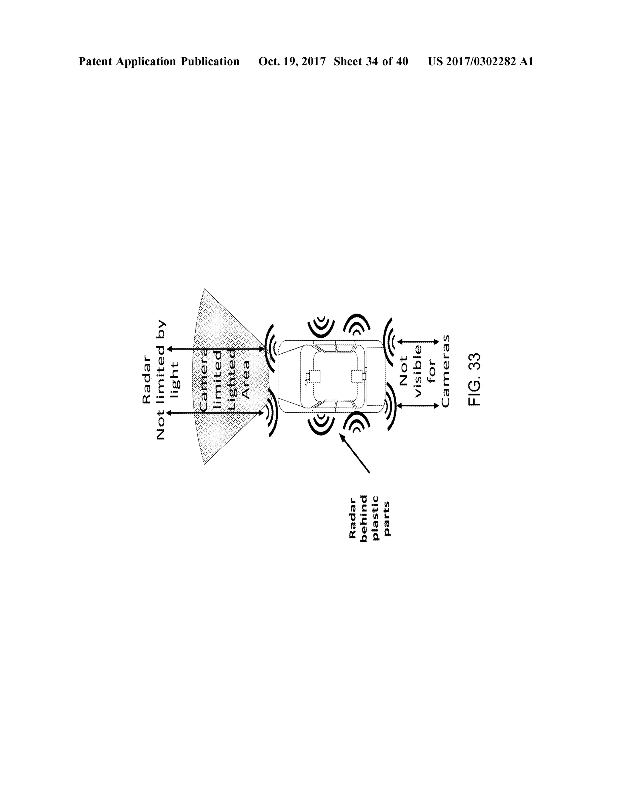
hand, are completely agnostic to lighting conditions and
perform the sameregardless of light (as shownin FIG . 33).
[0028] Passive visual sensing is very limited in adverse
weather conditions such as heavy rain , fog or snow ; Radar
systems aremuch more capable ofhandlingthesesituations.
Passive visualsystems create great amounts ofdata aswell
which needs to be handled in real time and thus require
expensive and complicated computation capabilities, while
Radar systemscreate much less data that is easier to handle.
Passive visual systems cannot see " through" objects while
Radar can, which is useful in determining if there are
hazardsbehind vegetation for instance such as wildlife that
is about to cross the road.
[0029] Further, it is easily understandable that in order to
cover all possible scenarios all (or most of these sensors
need to work together as a well-tuned orchestra . But even if
that is the case,underadverse lightingandweather condition
some sensor types suffer from performance degradation
while the Radar performance stays practically stable under
allofthese conditions. Thepractical conclusion is thatRadar
performance is not driven by environmental factors asmuch
as by its own technology deficiencies, or a specific defi
ciency of one of its internal components that the invention
here will solve.
[0030] Summarizing all ofthe advantages and disadvan
tages mentioned above it is clear that Radar systems are
efficient in termsof cost,weight, size and computing power.
Radar systems are also very reliable under adverse weather
conditions and allpossible lighting scenarios. Further, SAR
Radar Systems may be implemented to create a detailed
picture of the surroundings and even distinguish between
different types ofmaterial.
[0031] However, the drawback of existing Radar sensors
was the impacton their accuracy due to the phase noise of
its frequency source, the synthesizer. Thus, an enhanced
system is required (for purposes such as for autonomous
vehicles) that may utilize benefits of Radar system by
mitigating/eliminating the corresponding existing draw
backs. For example, the required enhanced system , in addi
tion to improving common existing Radar systems,should
also improve bistatic ormultistatic Radar designs that use
the same platform or different platforms to transmit and
receive for reducing the phase ambiguity that is created by
the distance of the transmitting antenna from the receiving
antenna by a significant amount.
[0032] Essentially,a signalthat is sentoutto coverobjects
(here: Radar Signal) is not completely spectrally clean but
sentoutaccompanied by phase noise in the shapeof“skirt”
in the frequency domain, and willmeet similar one in the
receiver signalprocessing once it is received back. In a very
basic target detection systems, fastmoving objects will shift
the frequency to far enough distance from the carrier so that
the weak signal that is being received will be outside of this
phase noise "skirt". Slow moving objects,however,such as
cars, pedestrians, bicycles, animals, etc. might create a
received signal that is closer to the carrier and weaker than](https://image.slidesharecdn.com/us20170302282a1-200617153345/75/Radar-target-detection-system-for-autonomous-vehicles-with-ultra-low-phase-noise-frequency-synthesizer-43-2048.jpg)
![US 2017/0302282 A1 Oct. 19,2017
relative to the receiver and f is the frequency shift that is
being created. After simplifying the equation,wewill get:
Af=42.5
thephase noise and this signalwillbeburied underthisnoise
and practically willbenon-detectable or non-recognizable.
[0033] More advanced systems use modulated signals
(such as FMCW ) but the same challenge to identify slow
moving objects remains. The determination of two physi
cally close objects vs. one larger object is also being
challenged by phase noise.
[0034] Anotheradvanced Radar System worthmentioning
is Synthetic aperture Radar (or SAR ) that is described in a
differentsection of this disclosure.
[0035] Many algorithms and methods have been devel
oped to filter out inaccuracies of Radar based imaging,
detection and other result processing. Some aremore com
putational intensive while others are not. The common to all
of them is that they are not able to filter out the inherent
phase noise of theRadar system itself
[0036] This iscrucial since a lotof theinformation aRadar
system relies on, is in thephase ofthe returning signal.One
simple example for this phenomenon is when a Radar signal
hits a wall that is perpendicular to the ground or a wall that
has an angle that is not 90 degree relative to the surface, the
phases ofthereturn signals willbeslightly different and this
information could be “buried” under the phase noise of the
Radar system .
0037] Further, speckle noise is a phenomenon where a
received Radar signal includes " granular” noise. Basically,
these granular dotsare createdby the sum ofallinformation
that is scattered back from within a “resolution cell” . All of
these signals can add up constructively, destructively or
cancel each other out. Elaborate filters and methods have
been developed ,butallofthem function better and with less
effort when the signals have a better spectral purity, or in
otherwordsbetter phase noise.One of these methods, just
as an example, is the “multiple look” method.When imple
menting this, each “ look” happens from a slightly different
point so that thebackscatter also looks a bit different. These
backscatters are then averaged and used for the final imag
ing. The downside of this is that themore “looks" are taken
the more averaging happens and information is lost aswith
any averaging.
[0038] As additionalbackground for this invention there
are few phenomena that need to be laid outhere:
[0039] Doppler Effect: The Doppler Effectis thechange in
frequency or wavelength of a wave for an observermoving
relative to its source. This is true for sound waves, electro
magnetic waves and any other periodic event.Most people
know about the Doppler Effect from their own experience
when they hear a car thatis sounding a siren approaching,
passingby and then receding. During theapproach the sound
waves get “ pushed” to a higher frequency and thus the siren
seems to have a higher pitch, and when the vehicle gains
distance this pitch gets lower since the sound frequency is
being “pushed” to a lower frequency.
[0040] The physical andmathematicalmodel ofthis phe
nomena is described in the following formula:
Where Av is the relativevelocity of the sound source to the
receiverand Af is the frequency shift created by the velocity
difference. It can easily be seen that when the velocity is
positive (the objects getcloserto each other)the frequency
shift willbe up. When the relative velocity is 0 , there willbe
no frequency shift at all, and when the relative velocity is
negative (the objects gain a distance from one another) the
frequency shift is down.
[0041] In old fashioned Radars the Doppler effect gets a
littlemore complicated since a Radar is sending outa signal
and expects to a receive signal that is lower in power but at
the same frequency when it hits an object. If this object is
moving, then this received signal will be subject to the
Doppler effect and in reality, the received signalwill notbe
received at the same frequency as the frequency of the
transmit signal. The challenge here is that these frequency
errors can be very subtle and could be obscured by the phase
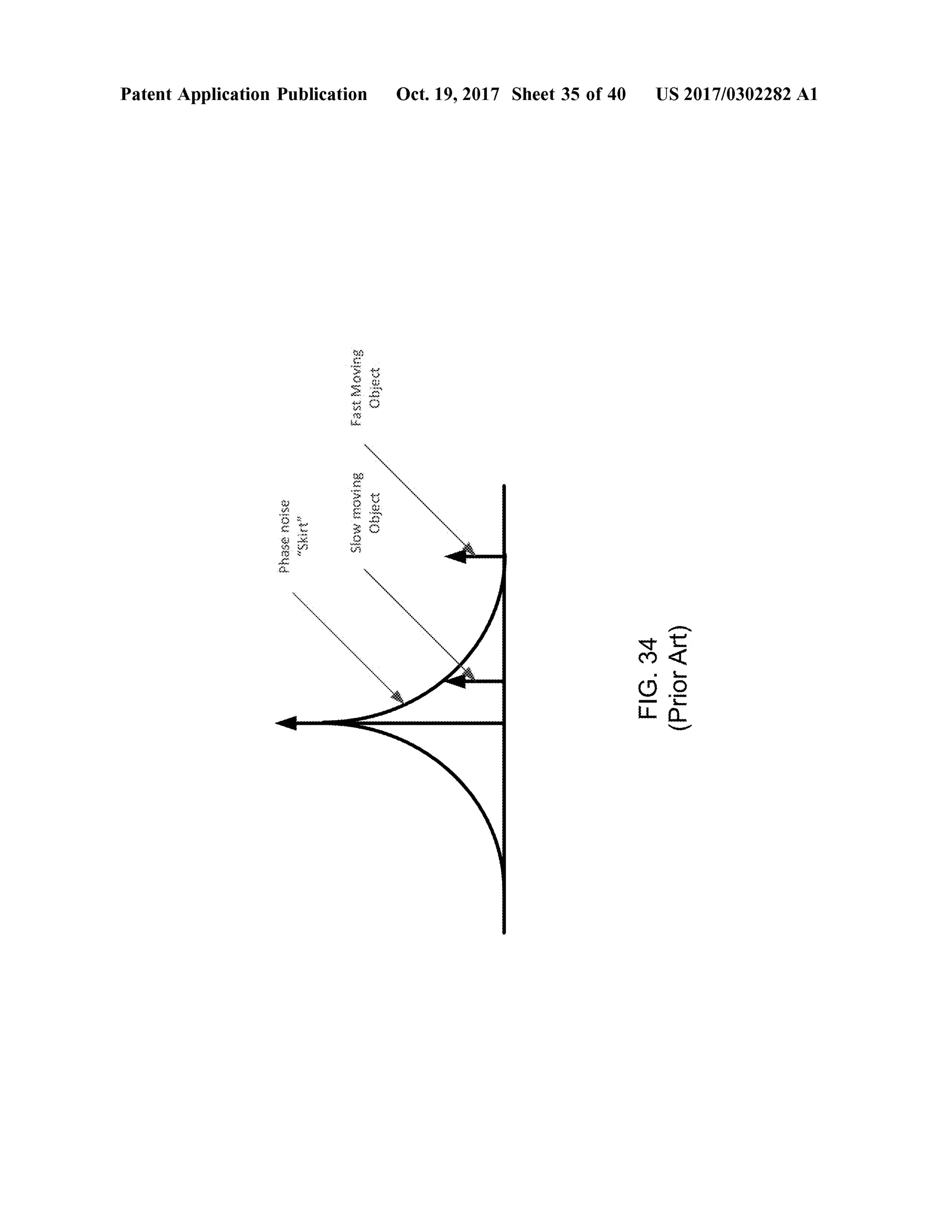
noise of the system (as shown in FIG . 34). The obvious
drawback is that vital information about the velocity of an
object gets lost only because of phase noise (see figure
below ). The above is especially right when dealing with
objects thatmove slower than airplanesandmissiles,such as
cars, bicycles, pedestrians, etc.
[0042] Modulated signals — Newer Radar systems use
modulated signals that are broadly called FMCW (Fre
quency Modulated Continuous wave), but they can come in
all forms and shapes such as NLCW , PMCW , chirps, etc.
(Nonlinear Continuous Wave and Phase Modulated Con
tinuous Wave). The main reason for the use ofmodulated
signals is that old fashioned Radars need to transmit a lotof
power to receive and echo back from a target while modu
lated signals and smart receive techniques can do thatwith
much lower transmitpower.
[0043] Another big advantage of FMCW based Radar
systems is that the distance of a target can be calculated
based on Affrom the instantaneous carrier signalrather than
travel time. However, herein also lies the problem to be
able to calculate and determine the characteristics of a target
accurately a spectrally clean signal with ultra -low phase
noise as low as technically possible provides many advan
tages.
100441 Usually modulated Radar signals are processed
with the help ofFFT utilizing signal processing windows
and pulse compression algorithms.While thesemethods are
good phasenoise stillremains one ofthemajorcontributors,
ifnotto say the largest contributor to errors and inaccura
cies.
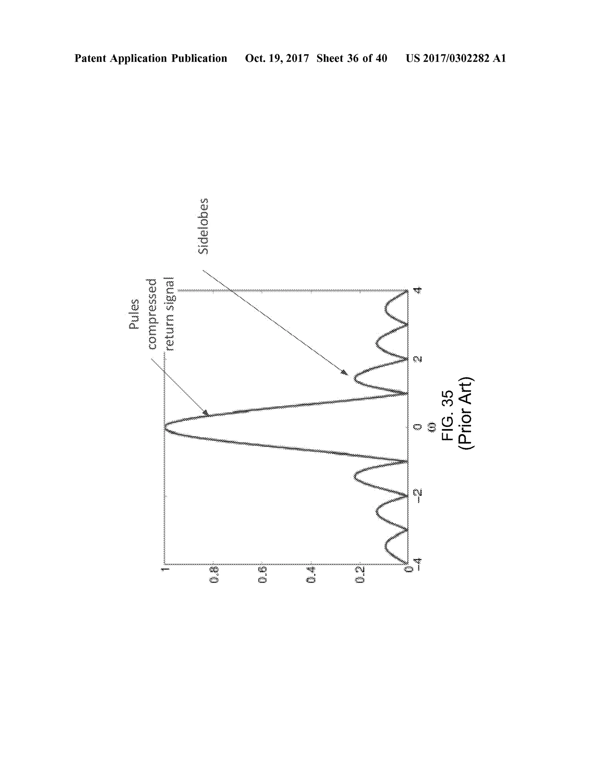
[0045] The spectralpicture ofa processed signallooks like
the FIG . 35. As one can see the spectral picture containsalso
unwanted sidelobes.Onemajor contributor to the sidelobes
is the phase noise of the Radar system . Phase noise (or
sometimes also called Phase Jitter or simply Jitter) responds
to 20 log integrated phase noise in rad). This spectral
regrowth of side lobes can cause errors in the determination
of the actual distance of a target, and can obscure a small
targetthat is close to a larger target. It can also cause errors
in target velocity estimation.
$=( AV)foTC + Vs
Where f,is the center frequency of the signal, c is the speed
of light, v , is the velocity of the receiver relative to the
sound/radiation source,v , isthevelocity ofthe sound source](https://image.slidesharecdn.com/us20170302282a1-200617153345/75/Radar-target-detection-system-for-autonomous-vehicles-with-ultra-low-phase-noise-frequency-synthesizer-44-2048.jpg)
![US 2017/0302282 A1 Oct. 19,2017
[0046] Another use of Radar that is sensitive to phase
noise includes Synthetic Aperture Radar (SAR ) ofall kinds.
These Radars are beingused in countless applicationsrang
ing from space exploration through earth 's surfacemapping,
Ice packmeasuring, forest coverage, variousmilitary appli
cations to urban imaging and archaeological surveys.How
ever,all the Radar applicationshave a common drawback of
bearing phase noise that leads to depletion of the quality of
the end-result or failure in achieving the desired outcome.
For example, whether we refer to Interferometric SAR
(InSAR)or Polarimetric SAR (POISAR ) or a combination of
thesemethods or any other typeofSAR or Radar in general,
all of them are suspect to phase noise effects regardless of
the type of waveform /chirp used. Considering the shift in
frequency and the low signal strength there is a probability
thatthe received Radar signalwillbeburied under thephase
noise skirt, and the slower theobject thisprobability grows.
Again , the determination of two close objects vs. one large
one is a challenge here. SAR Radars create images of their
surroundings and the accuracy of the images depends also
on the phase noise of the signal. Some of these radars can
also determine electromagnetic characteristics of their target
such as thedielectric constant, loss tangent etc. The accuracy
here again depends on the signal quality which is largely
determined by the sidelobes created duringthe utilization of
the FFTalgorithm mentioned abovewhich in turn stem from
the phase noise of the system .
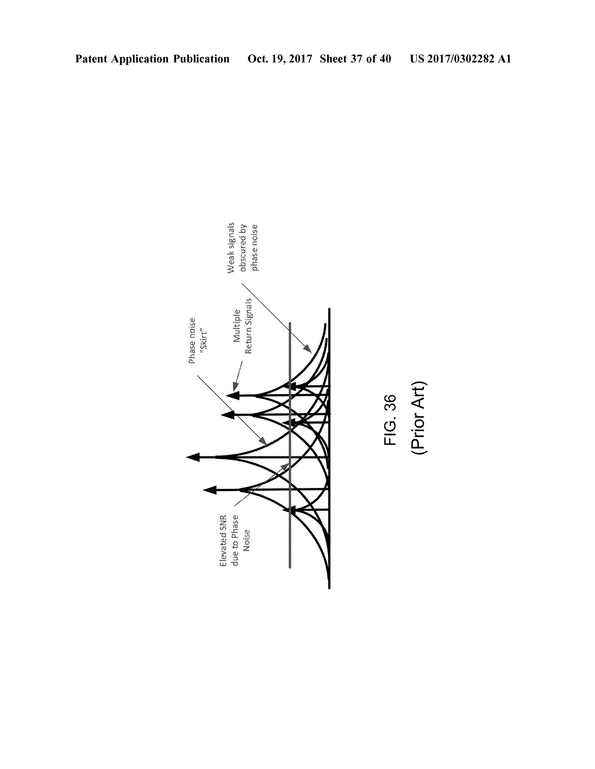
[0047] Further, in FIG . 36 , the sidelobes have been sim
plified to only a wide overlapping area. This is also very
close to what happens in reality because of the way the
signal processing algorithmswork. As can be easily seen in
the figure above,weaker return signals can get obscured in
the sidelobes of a stronger signal and the overall available
and crucial SNR decreases because every return signal
carries sidelobes with it.
[0048) Thus, the Radarsystemsare challenged when deal
ing with slow moving objects such as cars, bicycles and
pedestrians. Furthermore, these traditional Radar systems,
whether using a modulated or non-modulated signal, have
difficulties identifying objects that are very close to each
other since one of them willbe obscured by the phase noise
of the system .
10049] Based on the aforementioned, there is a need of a
radar system thatcan effectivelybe utilized forautonomous
cars by canceling or reducing the phase noiseofthereceived
Radar signal. For example, the system should be capableof
determining surroundings (such as by detecting objects
therein )with costeffectiveness and withoutsignificant inter
nalphase noise affecting performance.
[0050] The system should beable to add as less as possible
phase noise to the received Radar signal. Further,the system
shouldbeableofdetecting andanalyzingthereceived signal
without being affected by the internal receiver phase noise
therefrom . Furthermore, the system should be capable of
implementing artificialintelligence to make smart decisions
based on the determined surrounding information.Addition
ally, the system should be capable to overcome the short
comings ofthe existing systems and technologies.
in terms of target detection accuracy and resolution and
because of this it can become the dominant sensor for the
handling ofautonomous cars. Herein , the Synthesizer dras
tically reduces the phase noise ofRadar signals so that such
Radar sensorwill be able to replace current sensor systems
at very low cost and with reliability at all lighting and
adverse weather conditions.
[0052] A system that utilizes an ultra low phase noise
synthesizer willbe able to provide data to a processor that
can determine the electromagnetic characteristics of an
objectwith sufficientaccuracy so that the system is able to
determine if the object is a living object such as a human
being or an animalor if it is inanimate. It will also be able
to provide data that is accurate enough to differentiate
between thematerial objects are made of such as differen
tiating between wood and stone for example.
10053) Further as a derivative of the capability to deter
mine the material an object is made of combined with the
electromagnetic waves capability to penetrate through many
materials an object detection system utilizing an ultra low
phase noise synthesizer will provide data that will enable a
processingunit(such asa specialized processoroftheobject
detection system ) to find objects that are visually obscured
by another objectand determine thematerialoftheobscured
and obscuring object. Thus the system may be able to find
a human behind a billboard or wildlife behind a bush or
determine that these are only 2 bush onebehind the other.
[0054] According to an embodiment ofthepresentdisclo
sure, an object detection system for autonomous vehicles.
The object detection system may include a radar unit
coupled to at least one ultra -low phase noise frequency
synthesizer, configured for detecting the presence ofone or
more objects in one or more directions, the radar unit
comprising: a transmitter for transmitting at leastone radio
signal to the one or more objects; and a receiver for
receiving the atleast one radio signal returned from the one
or more objects. Further, the object detection system may
include the at least one ultra -low phase noise frequency
synthesizer thatmay be utilized in conjunction with the
radarunit, for refiningboth the transmitted and the received
signals,and thus determining thephase noise and maintain
ing the quality of the transmitted and the received radio
signals, wherein the at least one ultra-low phase noise
frequency synthesizer comprises: (i) at least one clocking
device configured to generate at least one first clock signal
ofat least one first clock frequency; (ii) at leastone sampling
Phase Locked Loop (PLL ), wherein the at least one sam
pling PLL comprises: (a ) at least one sampling phase detec
tor configured to receive the at least one first clock signal
and a single reference frequency to generate atleast one first
analog controlvoltage;and (b)at least onereference Voltage
Controlled Oscillator (VCO ) configured to receive the at
least one analog control voltage to generate the single
reference frequency; and (c) a Digital Phase/Frequency
detector configured to receive the at least one first clock
signal and a single reference frequency to generate at least
a second analog control voltage; and (d ) a two-way DC
switch in communication with the Digital Phase/Frequency
detector and the sampling phase detector; (iii) at least one
first fixed frequency dividerconfigured to receive the at least
one reference frequency and to divide the at least one
reference frequency by a first predefined factor to generate
at least one clock signal for at leastone high frequency low
phase noise DirectDigitalSynthesizer (DDS) clock signal;
SUMMARY
[0051] Someofthebenefits of the invention: The present
invention emphasizes that by incorporating the ultra -low
phase noise synthesizer in existing Radar system , the per
formance oftheRadar system willbe improved substantially](https://image.slidesharecdn.com/us20170302282a1-200617153345/75/Radar-target-detection-system-for-autonomous-vehicles-with-ultra-low-phase-noise-frequency-synthesizer-45-2048.jpg)
![US 2017/0302282 A1 Oct.19,2017
(iv) at least one high frequency low phase noise DDS
configured to receive the at least oneDDS clock signal and
to generate at least one second clock signal of at least one
second clock frequency; and (v) at least one main Phase
Locked Loop (PLL ).
[0055] Hereinabove, the main PLL may include: (a ) at
least one high frequency DigitalPhase/Frequency detector
configured to receive and compare the at least one second
clock frequency and at least one feedback frequency to
generate at least one second analog control voltage and at
least one digital controlvoltage; (b ) at least one main VCO
configured to receive the at least one first analog control
voltage or the at least one second analog control voltage and
generate at least one output signal of at least one output
frequency, wherein the at least one digital control voltage
controlswhich of the at least one first analog control voltage
or the at least one second analog control voltage is received
by the at leastone main VCO ; (c ) atleastone down convert
mixer configured to mix the at least one output frequency
and the reference frequency to generate at least one inter
mediate frequency; and (d ) at least one second fixed fre
quency divider configured to receive and divide the at least
one intermediate frequency by a second predefined factor to
generate the at least one feedback frequency.
[0056] Herein, the radar unitdetermines a distance and a
direction of each ofone or more objects. Further, the radar
unit determines one or more characteristics, of two close
objects irrespective ofsize ofthe one ormore objects.Again
further, the radar unit differentiates between two ormore
types of the objects when one object is visually obscuring
another object. Additionally, the radar unit utilizes amodu
lated or non-modulated radio signal, to determine presence
of a slow moving target despite the very small Doppler
frequency shift.Also, the radar unit utilizes a modulated or
non -modulated radio signal, to determine presenceofa close
range targetdespite the very short signal travel time.
[0057] The object detection system may further include at
least one additional sensor system , available on the autono
mousvehicle, in conjunction with theradarunit.Further,the
at least one ultra -low phase noise frequency synthesizer
further comprises at least one fixed frequency multiplier
configured to receive and multiply the at least one output
signal generated by the at least one main PLL by a pre
defined factor to generate at least one finaloutput signal of
at least one finaloutput frequency. The atleast oneultra-low
phase noise frequency synthesizer is implemented on the
same electronic circuitry or on a separate electronic cir
cuitry. Further, the ultra-low phase noise frequency synthe
sizermay be used to generate the up or down converting
signal ofthe radar unit.
[0058] Further, according to another embodiment of the
present disclosure, a method for autonomous vehicles is
disclosed. The method may include (but is not limited to ):
detecting a presence of one ormore objects in one ormore
directionsby a radar unit.Herein, the radar unit comprising:
a transmitter for transmitting at least one radio signal to the
one ormore objects,and areceiver forreceivingthe at least
one radio signal returned from the one or more objects .
Further,themethod may includeperforming,by atleastone
ultra-low phase noise frequency synthesizer for refining the
transmitted and the received signals, and thereby determin
ing a phase noise andmaintaining quality ofthe transmitted
and the received radio signals.
[0059] Hereinabove, theatleastone ultra-low phase noise
frequency synthesizer comprises: (i) at least one clocking
device configured to generate at least one first clock signal
ofatleastone first clock frequency; (ii) atleast onesampling
Phase Locked Loop (PLL), wherein the at least one sam
pling PLL comprises: (a)atleast one sampling phase detec
tor configured to receive the at least one first clock signal
and a single reference frequency to generate at leastone first
analogcontrol voltage;and (b ) atleastone reference Voltage
Controlled Oscillator (VCO ) configured to receive the at
least one analog control voltage to generate the single
reference frequency; and (c) a Digital Phase/Frequency
detector configured to receive the at least one first clock
signal and a single reference frequency to generate at least
a second analog control voltage; and (d ) a two-way DC
switch in communication with theDigitalPhase/Frequency
detector and the sampling phase detector; (iii) at least one
first fixed frequency divider configured to receive theatleast
one reference frequency and to divide the at least one
reference frequency by a first predefined factorto generate
at least one clock signal for at least one high frequency low
phase noise Direct Digital Synthesizer (DDS) clock signal;
(iv ) at least one high frequency low phase noise DDS
configured to receive the at least oneDDS clock signaland
to generate at least one second clock signal ofat least one
second clock frequency; and (v) at least one main Phase
Locked Loop (PLL ), wherein the at least one main PLL
comprises: (a) at least one high frequency Digital Phasel
Frequency detector configured to receive and compare the at
least one second clock frequency and at least one feedback
frequency to generate at least one second analog control
voltage and at least one digital control voltage; (b ) at least
onemain VCO configured to receive the at least one first
analog control voltage or the at least one second analog
control voltage and generate at least one output signal of at
least one output frequency,wherein the at least one digital
control voltage controlswhich of the at least one firstanalog
control voltage or the at least one second analog control
voltage is received by the atleast onemain VCO ; (c) at least
one down convert mixer configured to mix the at least one
output frequency and the reference frequency to generate at
least one intermediate frequency; and (d ) at leastone second
fixed frequency divider configured to receive and divide the
at least one intermediate frequency by a second predefined
factor to generate the at least one feedback frequency.
[0060] Herein , the method may further include various
steps such as receiving and multiplying,byultra-low phase
noise frequency synthesizer, the at leastone outputsignalby
a predefined factor to generate at least one finaloutput signal
ofat least one finaloutput frequency. Further, themethod
may generate theup converting or down converting signalof
the radar unit. Furthermore, the method may determine
presence of a slow moving target despite the very small
Doppler frequency shift. Again further, the method may
include determining presence of a close range targetdespite
the very short signal travel time. Additionally, the method
may determine a distanceand a direction ofeach ofthe one
ormore objects. Furthermore, themethod may determine a
type ofmaterial an object is made up of Also, the method
may include a step of activating one ormore additional
sensors for operation thereof in conjunction with the radar
unit. Themethod may determine characteristics of two close
objects irrespective of size of the objects. Further, the](https://image.slidesharecdn.com/us20170302282a1-200617153345/75/Radar-target-detection-system-for-autonomous-vehicles-with-ultra-low-phase-noise-frequency-synthesizer-46-2048.jpg)
![US 2017/0302282 A1 Oct. 19,2017
methodmay differentiate between two ormore types of the
objects when oneobject is visuallyobscuringanother object.
[0061] According to an embodiment of the present disclo
sure, a system is a detection system that comprises a radar
unit, communicably coupled to at least one ultra -low phase
noise frequency synthesizer, is provided. The radar unit
configured for detecting the presence ofone ormore objects
in one ormore directions.Herein, the radar unit comprising:
a transmitter for transmitting at least one radio signal; and a
receiver forreceiving at least oneradio signal returned from
one or more objects/targets. Further, the detection system
may include at least one ultra-low phase noise frequency
synthesizer thatmaybe configured for refining thereturning
the atleast oneradio signalto reduce phase noise therefrom .
[0062] Herein, the ultra-low phase noise frequency syn
thesizeris a criticalpartofa System , regardless ofhow it is
implemented. The ultra -low phase noise frequency synthe
sizer comprisesone main PLL (Phase Lock Loop) and one
reference sampling PLL. Themain PLL comprises one high
frequency DDS (Direct Digital Synthesizer), one Digital
Phase Frequency Detector, onemain VCO (Voltage Con
trolled Oscillator), one internal frequency divider, one out
put frequency divider or multiplier and one down convert
mixer. The reference sampling PLL comprises one reference
clock,one sampling phasedetector,and one reference VCO.
This embodimentprovides vast and critical improvement in
the overall system output phase noise. The synthesizer
design is based on the following technical approachesa )
using ofdual loop approach to reduce frequency multipli
cation number, b) using of sampling PLL as the reference
PLL to make its noise contribution negligible, c) using of
DDS to provide high frequency input to the main PLL and
d )usingofhigh frequencyDigitalPhase Frequency Detector
in the main PLL.
[0063] According to an embodiment of the present disclo
sure a detection system comprising a radar unit and an
ultra -low phasenoise frequency synthesizer is provided. The
system ismade up of System on Chip (SOC ) module. The
radar unit configured for detecting the presence of one or
more objects in one or more directions. The radar unit
comprising: a transmitter for transmitting atleast one radio
signal; and a receiver for receiving the at least one radio
signal returned from the one or more objects/targets. In an
embodiment, the Transmit and receive signal frequencies
mightbe equal. For example, if there is no Doppler effect,
the signal frequenciesmay be equal. In an embodiment the
transmit and receive frequenciesmight also be different, for
example in cases where the Doppler Effect is present. The
ultra -low phase noise frequency synthesizer comprises one
main PLL (Phase Lock Loop) and one reference sampling
PLL. The main PLL further comprises one Fractional-N
Synthesizer chip, one primary VCO (Voltage Controlled
Oscillator) and one down convertmixer. The Fractional-N
Synthesizer chip includes one Digital Phase Detector and
one software controllable variable frequency divider. The
reference sampling PLL comprises one sampling PLL, and
one reference VCO . This embodiment provides multiple
improvements in system output which are based on the
following technical approaches— a) using of dual loop
approach to reduce frequency multiplication number, b )
using of sampling PLL to make its noise contribution
negligible, and c) using of a high frequency Fractional-N .
Synthesizer chip in the main PLL.
[0064] In an additional embodiment ofthe presentdisclo
sure, a vehicle having a detection system is disclosed. The
detection system may be implemented for detecting infor
mation corresponding to one ormore objects, thedetection
unit comprising: a radar unit for transmitting radio signals
and further forreceiving the returned radio signal(s) from
one ormore objects/targets;and at least one ultra -low phase
noise frequency synthesizer for refining thereturned signals
to reduce the effect of phase noise in the returned radio
signals.Further,the detection unit comprises a processor for
processing the refined signals to determine one or more
characteristics correspondingto theoneormore objects, the
processor determining one ormore actions based on one or
more factors and the oneormore characteristics correspond
ing to the one ormore objects. The processor further may
determine one or more actions being adoptable by the
vehicle based on one or more characteristics that may
originate from the radar system and/or in conjunction with
information originated from another sensor. The vehicle
further includes one or more components communicably
coupled to the processor forperforming the determined one
ormore actions.
[0065] The detection system may further include a
memory for storing information and characteristics corre
sponding to the one ormore objects; and actionsperformed
by the vehicle.
[0066] Hereinabove, the atleastoneultra-low phase noise
frequency synthesizer may be implemented in any manner
as described further in the detailed description of this
disclosure. Further, the radar unit comprises at least one of:
traditional single antenna radar, dual ormulti antenna radar,
synthetic aperture radar, and one or more other radars.
Further, in an embodiment, the processor may determine
phase shift in frequencies of the transmitted radio signals
and the returned radio signals. Such phase shift (difference
in phase noise frequency)may further be analyzed in light
of a frequency of the refined radio signal to self-evaluate
overall performance of the detection system (or specific
performance of theultra-low phase noise frequency synthe
sizer).
100671. The preceding is a simplified summary to provide
an understanding of some aspects ofembodiments of the
presentdisclosure. This summary is neither an extensive nor
exhaustive overview ofthepresentdisclosure and its various
embodiments. The summary presents selected concepts of
the embodiments of the present disclosure in a simplified
form as an introduction to the more detailed description
presented below . Aswillbe appreciated, other embodiments
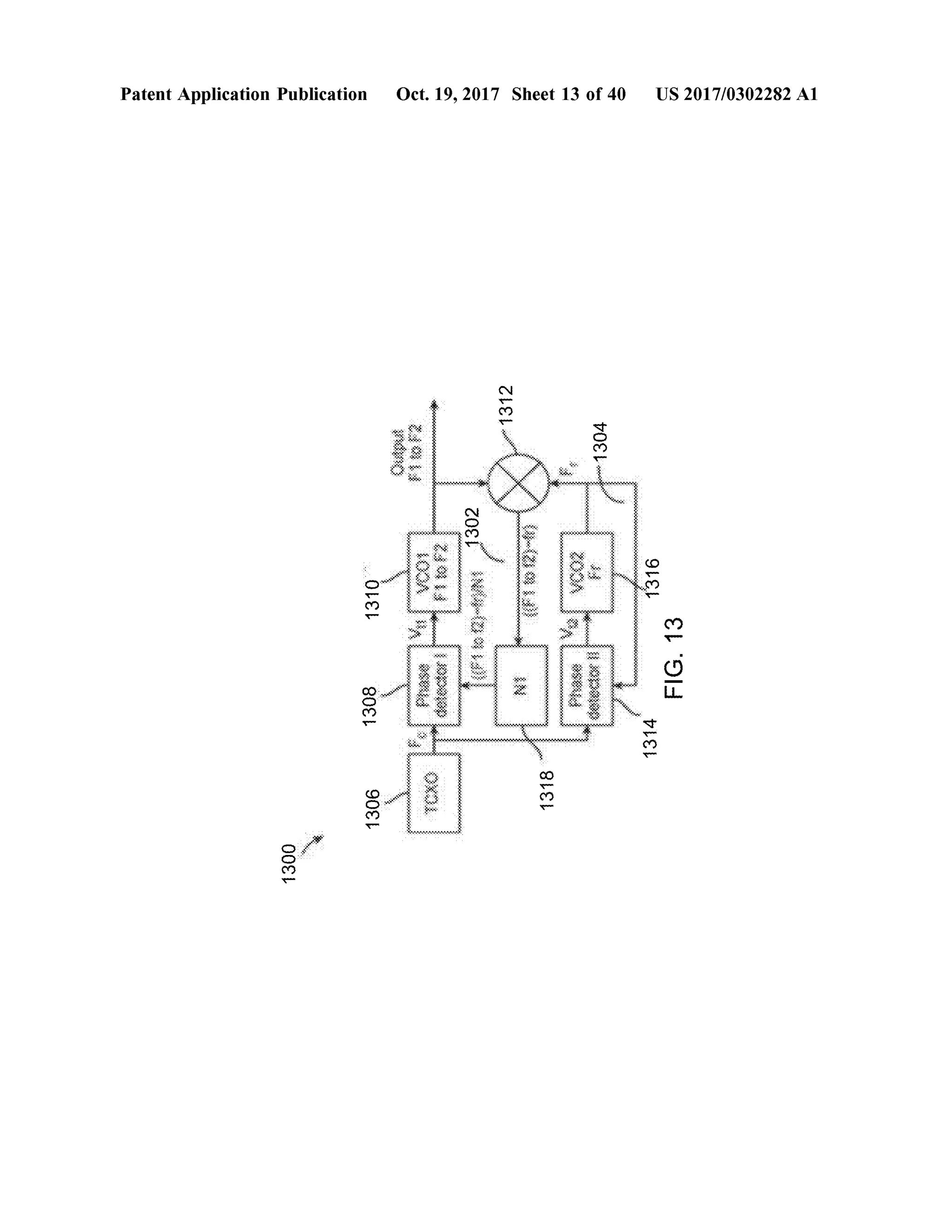
ofthe presentdisclosure arepossible utilizing,alone or in
combination, one or more of the features set forth above or
described in detail below .
BRIEF DESCRIPTION OF THE DRAWINGS
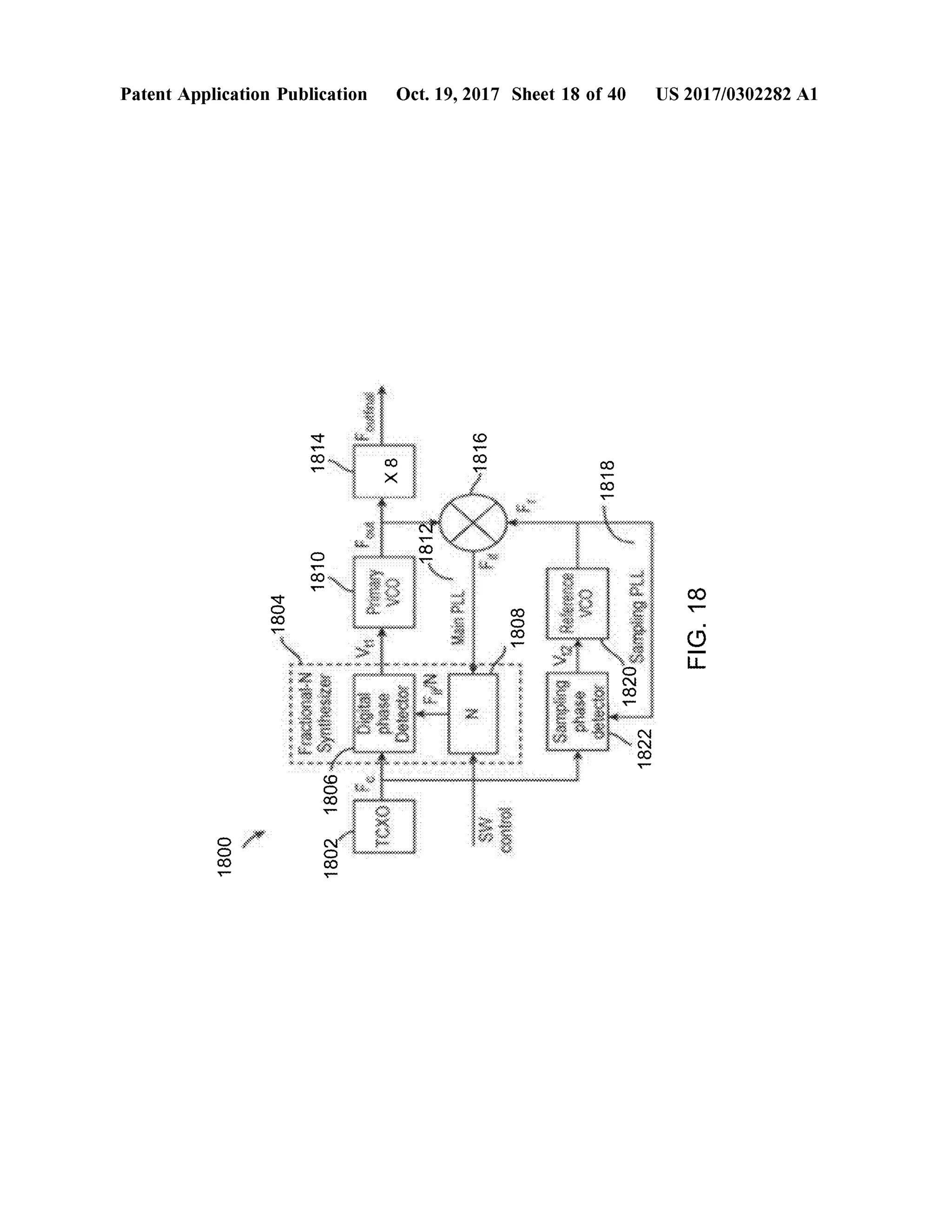
[0068] The above and still further features and advantages
ofembodiments of thepresent invention willbecomeappar
ent upon consideration of the following detailed description
ofembodiments thereof, especially when taken in conjunc
tion with the accompanying drawings,and wherein:
[0069] FIG . 1 illustrates a general block diagram of a
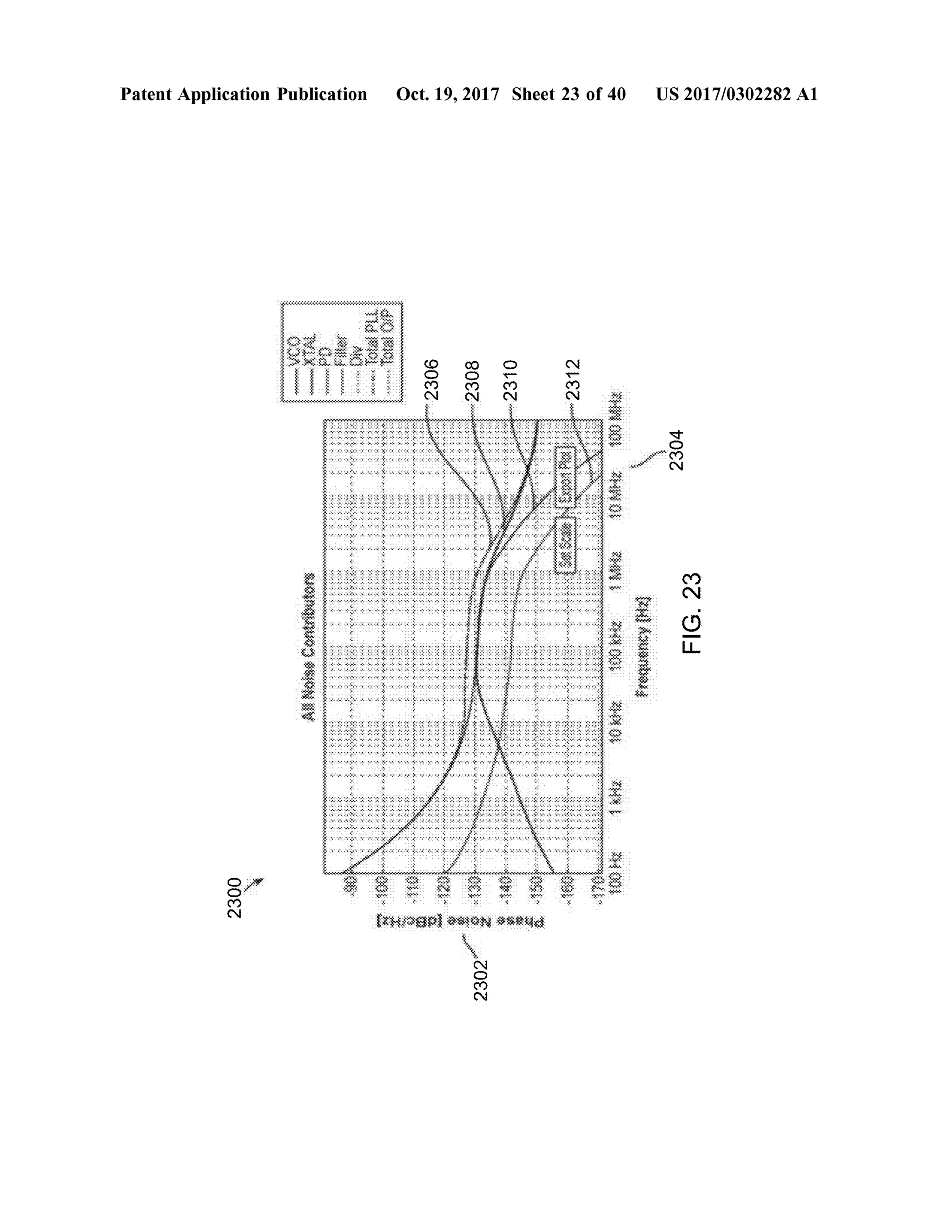
negative feedback system ;
[0070] FIG . 2 illustrates a general block diagram of a
standard Phase Lock Loop (PLL) ;
[0071] FIG . 3 illustrates a simplified drawing of a digital
phase/frequency detector;](https://image.slidesharecdn.com/us20170302282a1-200617153345/75/Radar-target-detection-system-for-autonomous-vehicles-with-ultra-low-phase-noise-frequency-synthesizer-47-2048.jpg)
![US 2017/0302282 A1 Oct. 19,2017
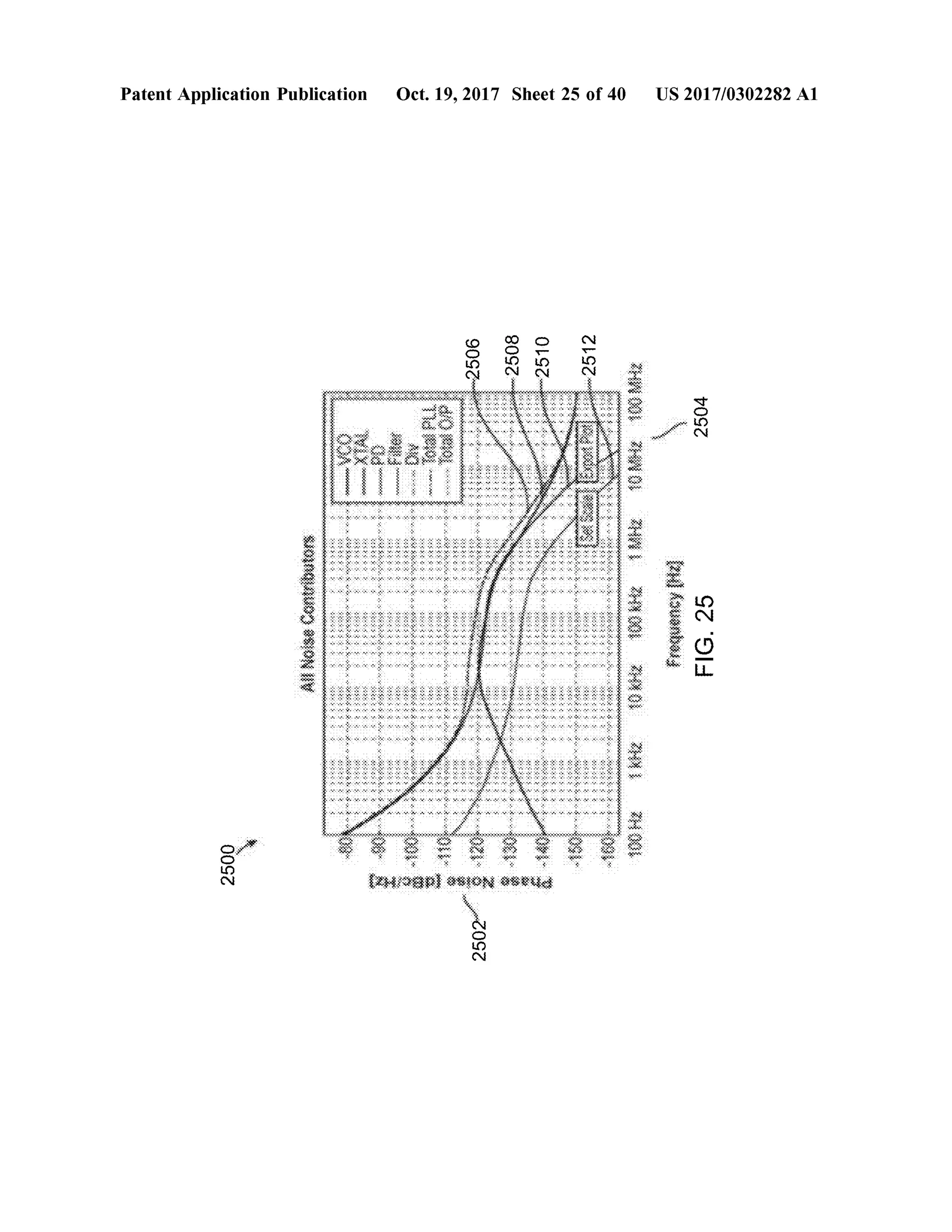
[0093] FIG . 25 illustrates a phase noise simulation plot
contributedby a reference sampling PLL having the TCXO
clock (or any other reference Clock ) generating input fre
quencies of 100 MHz in accordance with the second
embodiment of the present disclosure;
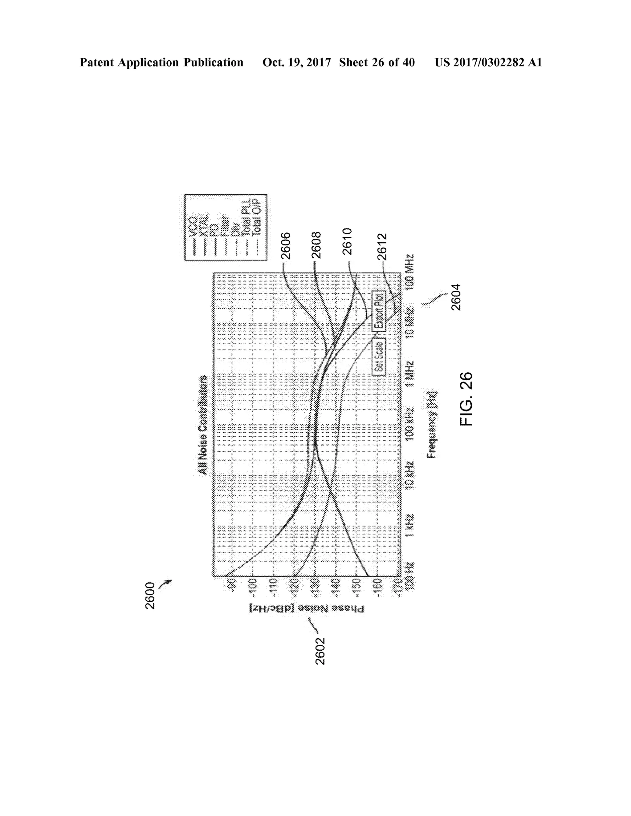
[0094] FIG . 26 illustrates a phase noise simulation plot
contributed by a reference sampling PLL having the TCXO
clock (or any other reference Clock ) generating input fre
quencies of 250 MHz in accordance with the second
embodimentof the presentdisclosure;
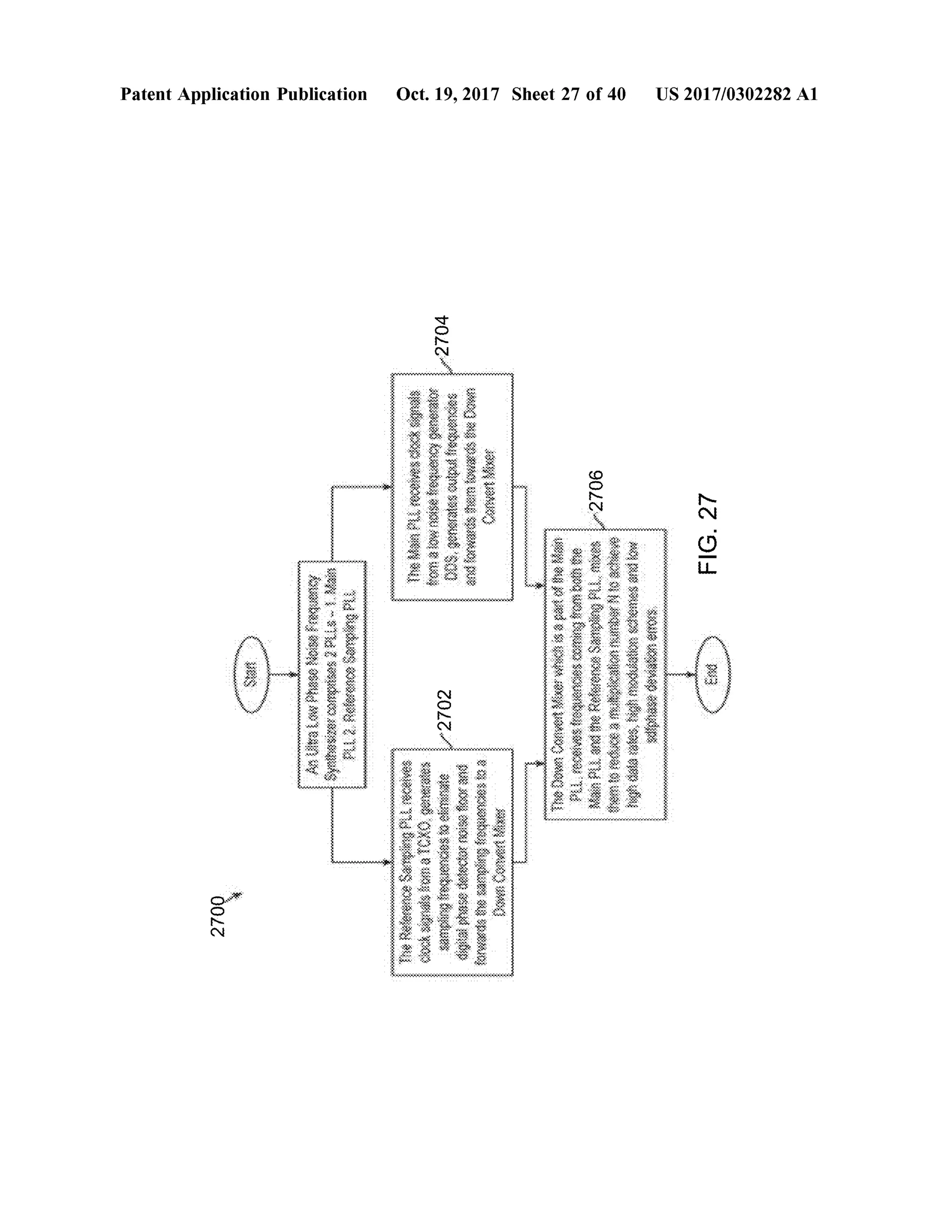
[0095] FIG . 27 illustrates a flow chartdepicting theopera
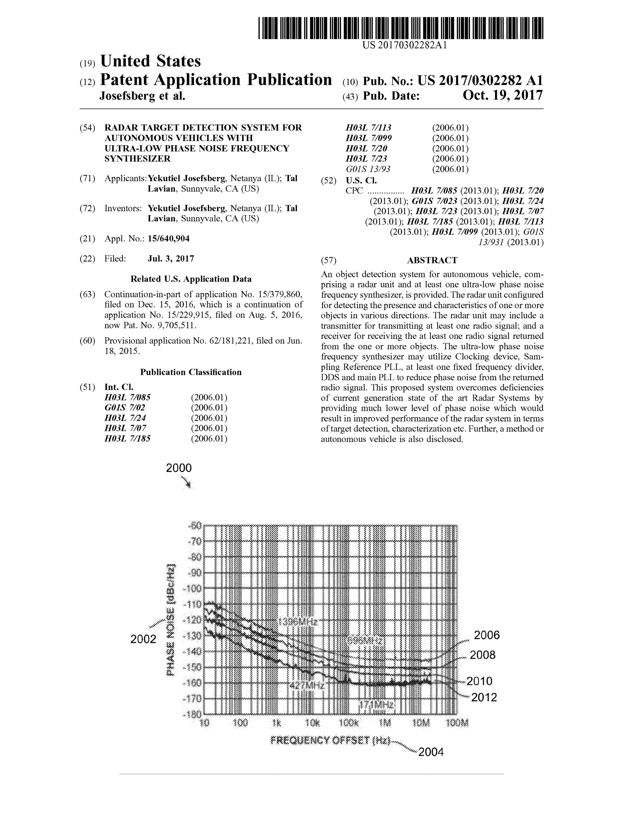
tionalmethod steps of the first embodiment;
0096) FIG . 28 illustrates a flow chart depicting the opera
tionalmethod steps of the second embodiment;
[0097] FIG .29 illustratesa flow chartdepicting the opera
tionalmethod steps of the sampling PLL;
[0098] FIGS. 30-36 correspond to prior arts and existing
technologies;
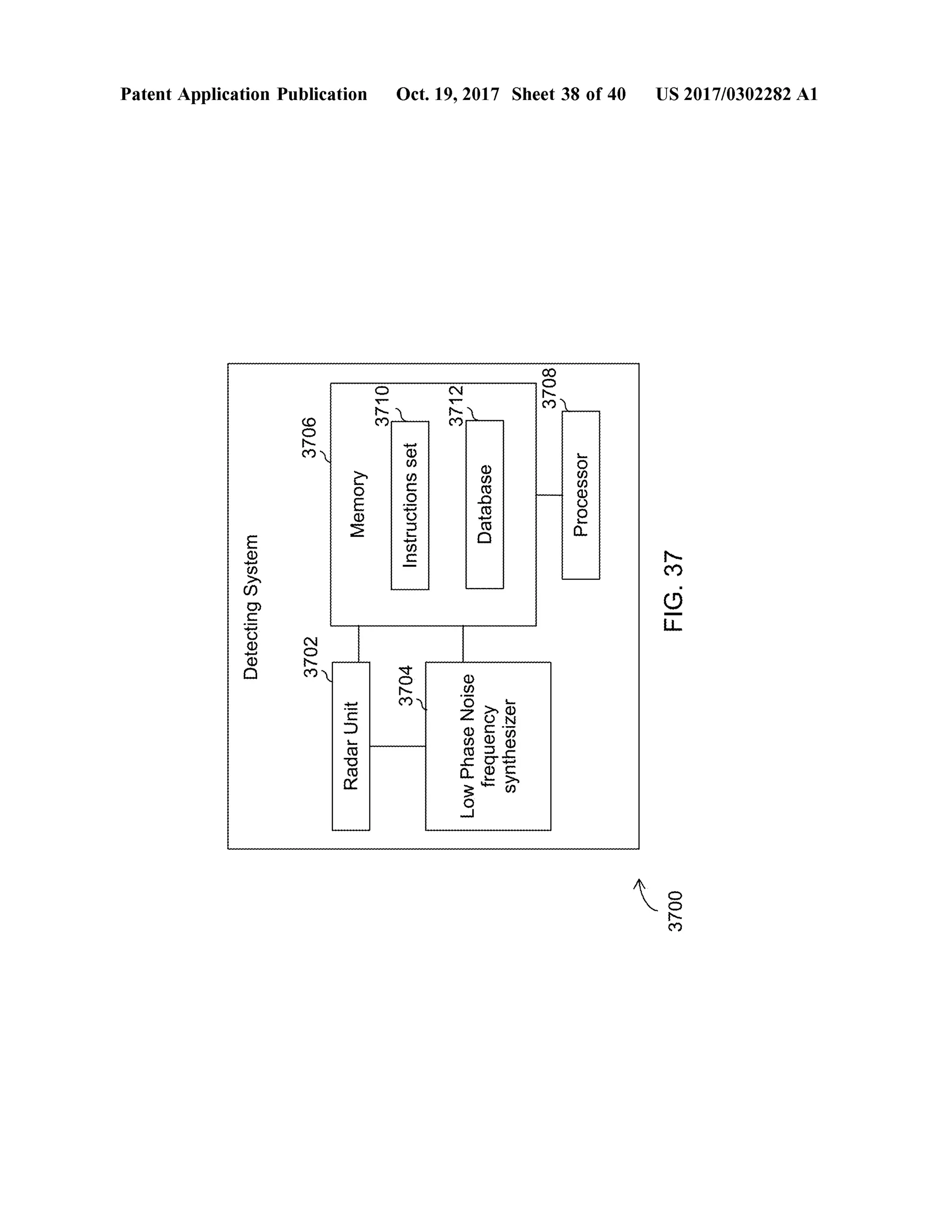
[0099] FIG . 37 illustrates a detection system , in accor
dance with various embodiments of the present invention ;
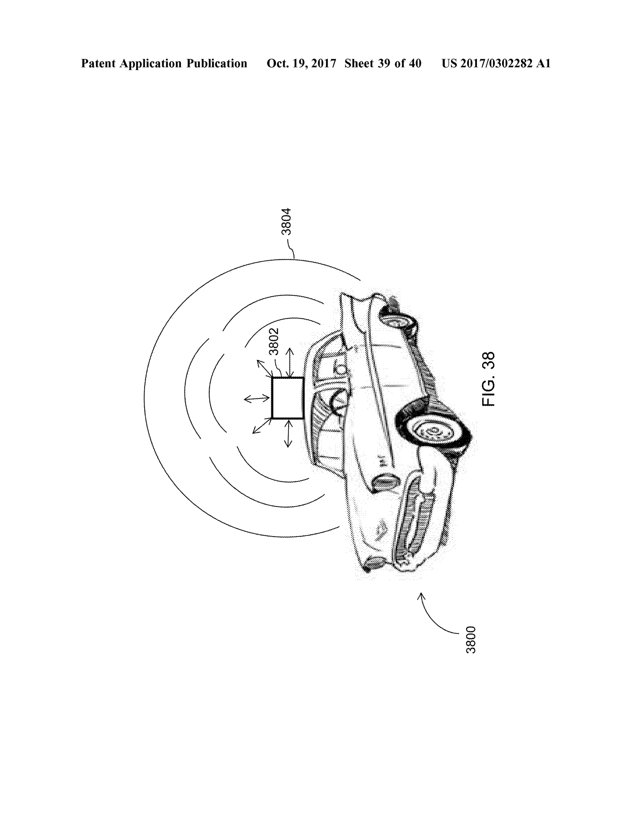
[0100] FIG . 38 illustrates an exemplary vehicle imple
menting detection system , in accordance with an embodi
ment of the present invention; and
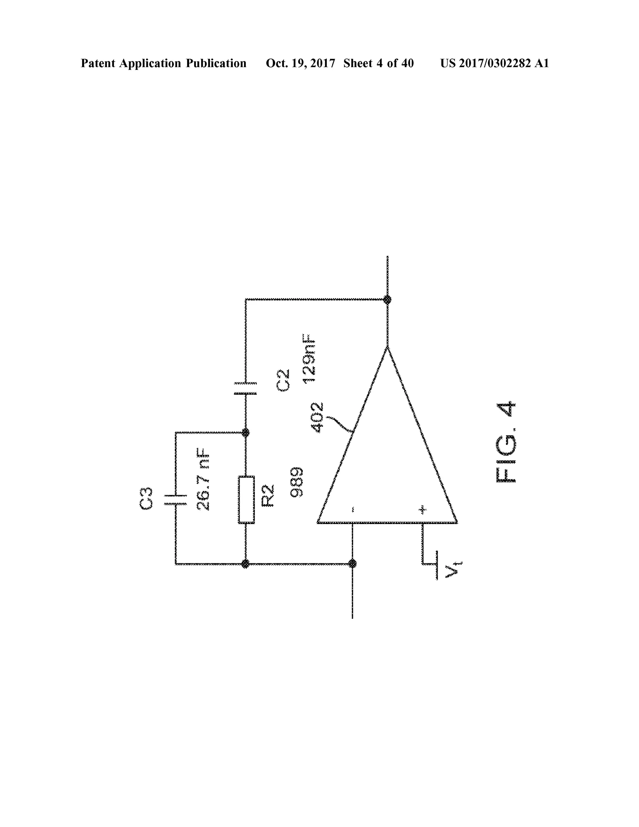
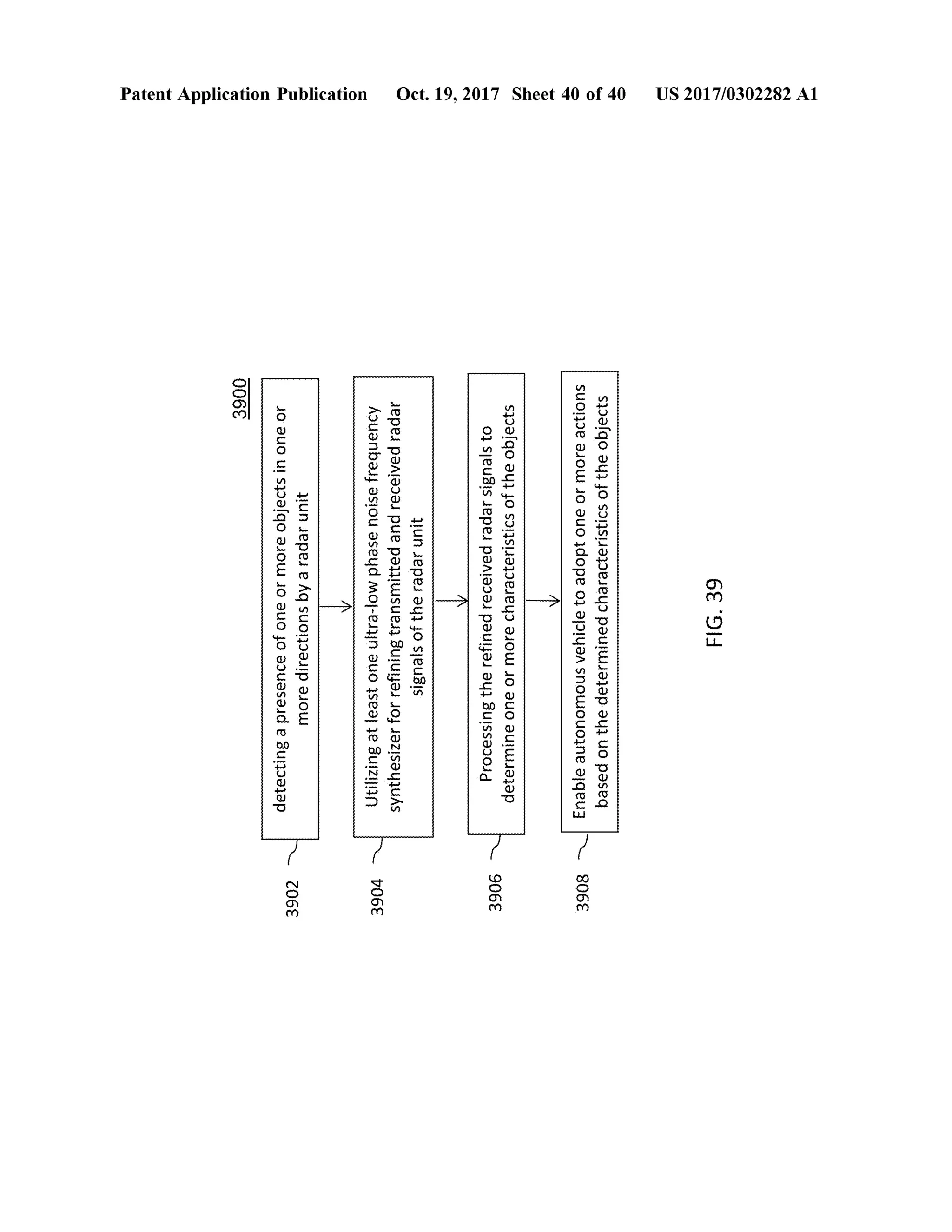
10101] FIG . 39 illustrates an exemplary method flow dia
gram for autonomous vehicle, in accordance with an
embodiment of the present invention.
10102] To facilitate understanding, like reference numerals
have been used, where possible, to designate like elements
common to the figures.
[0072] FIG . 4 illustrates an example of an active filter as
applied to a general PLL;
[0073] FIG . 5 illustratesthe principle of sample-and-hold
mechanism ;
[0074] FIG . 6 illustrates a schematic ofthe step recovery
diodeas comb generator feeding the dualschottky diode that
acts as phase detector;
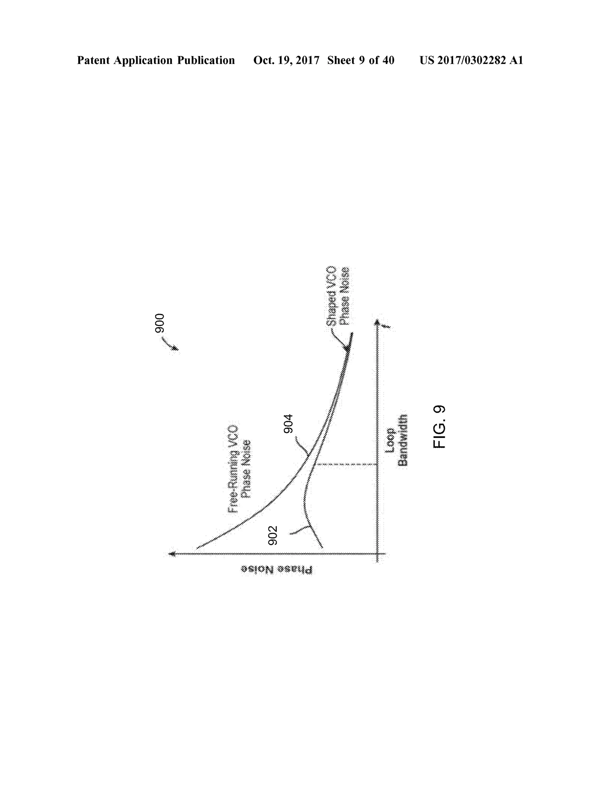
[0075] FIG . 7 illustrates a complete example schematic of
the comb generator and sampling phase detector with RF
pre-amplifier and two DC buffers following the phasedetec
tor;
[0076 ] FIG . 8 illustrates a phase noise plotof an example
free running Voltage Control Oscillator (VCO ) in the fre
quency domain (spectrum analyzer),withoutbeinglockedin
a PLL;
[0077] FIG . 9 illustratesa phasenoise plotofan example
Voltage ControlOscillator (VCO ) in the frequency domain
(spectrum analyzer),compensated bybeinglockedin a PLL;
[0078] FIG . 10 illustrates two plots: (a ) a simulation of
phase noise of an example PLL, and (b) is an actual
measurement;
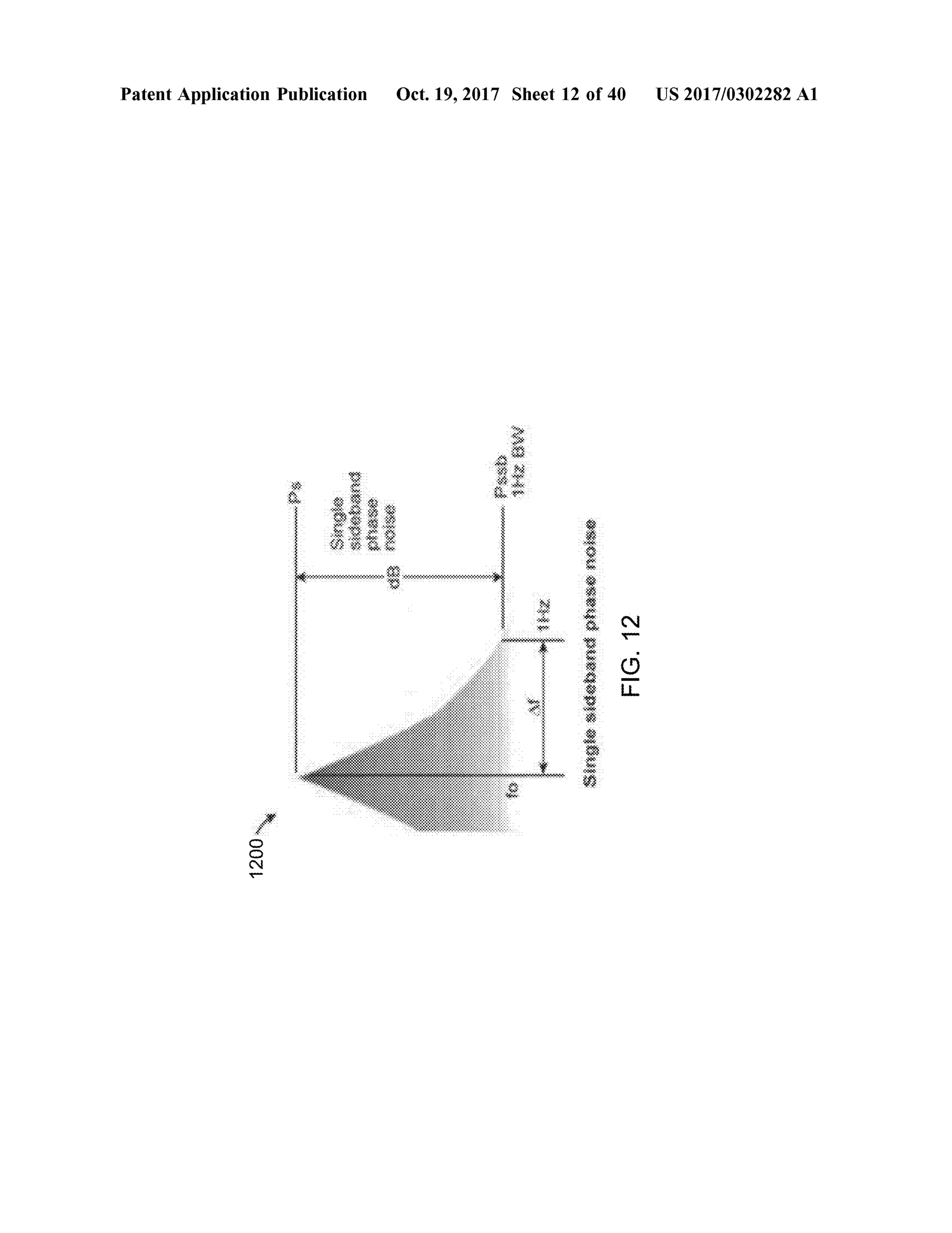
10079 ) FIG . 11 illustrates a phase noise plot of a closed
loop PLL , showing clearly the effect of the phase detector
multiplication number 20* LOG (N ) within loop bandwidth;
[0080] FIG . 12 illustrates a plotofmeasurement termsof
phasenoise in 1 Hzbandwidth at a Afoffset frequency from
the carrier.
[0081] FIG . 13 illustrates a general block diagram ofan
example dual loop PLL;
[0082] FIG . 14 illustrates a general block diagram of an
example dual sampling PLL;
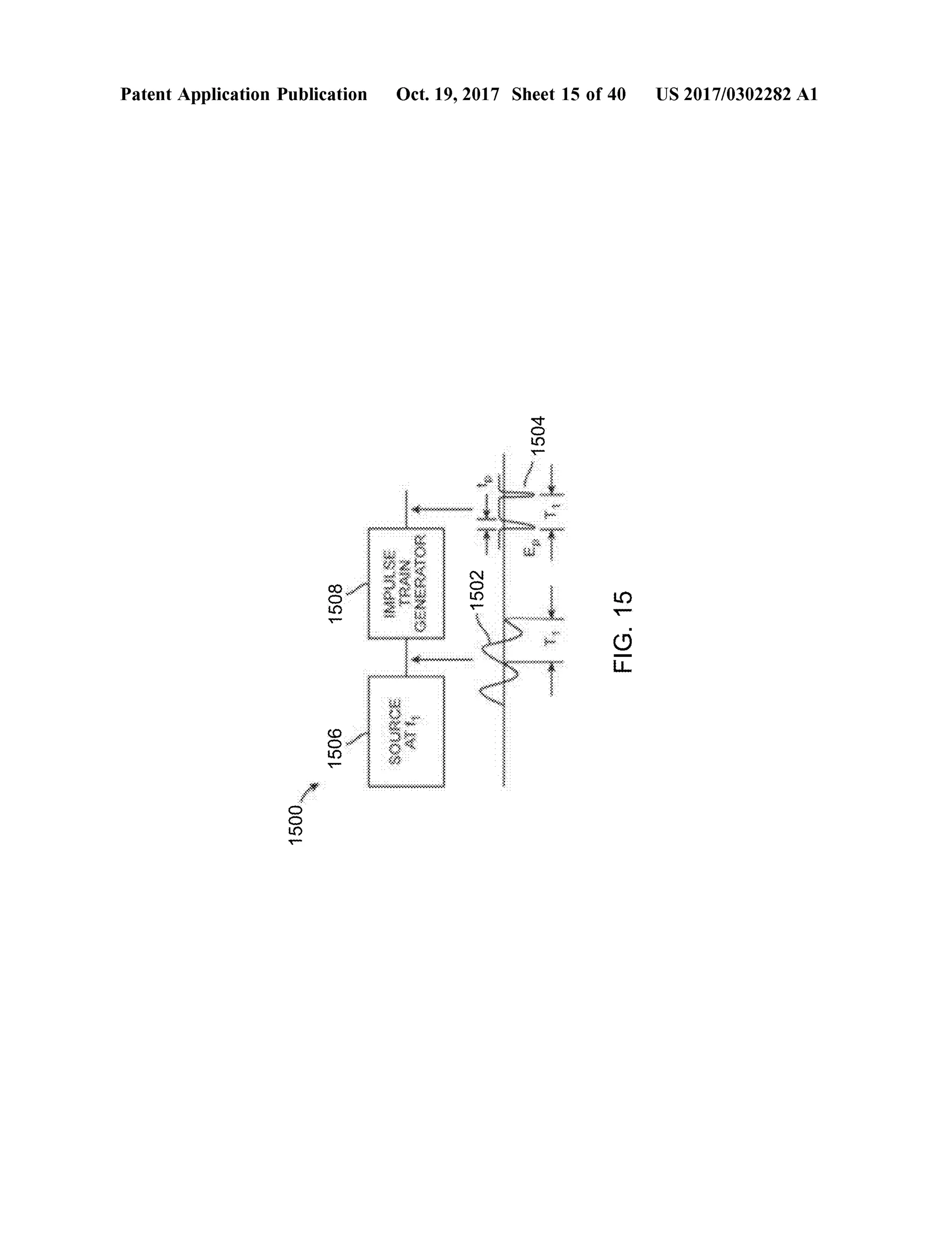
[0083] FIG . 15 illustrates how impulse or " comb” genera
tor changes a wave shape of a signal from sine wave to
pulses;
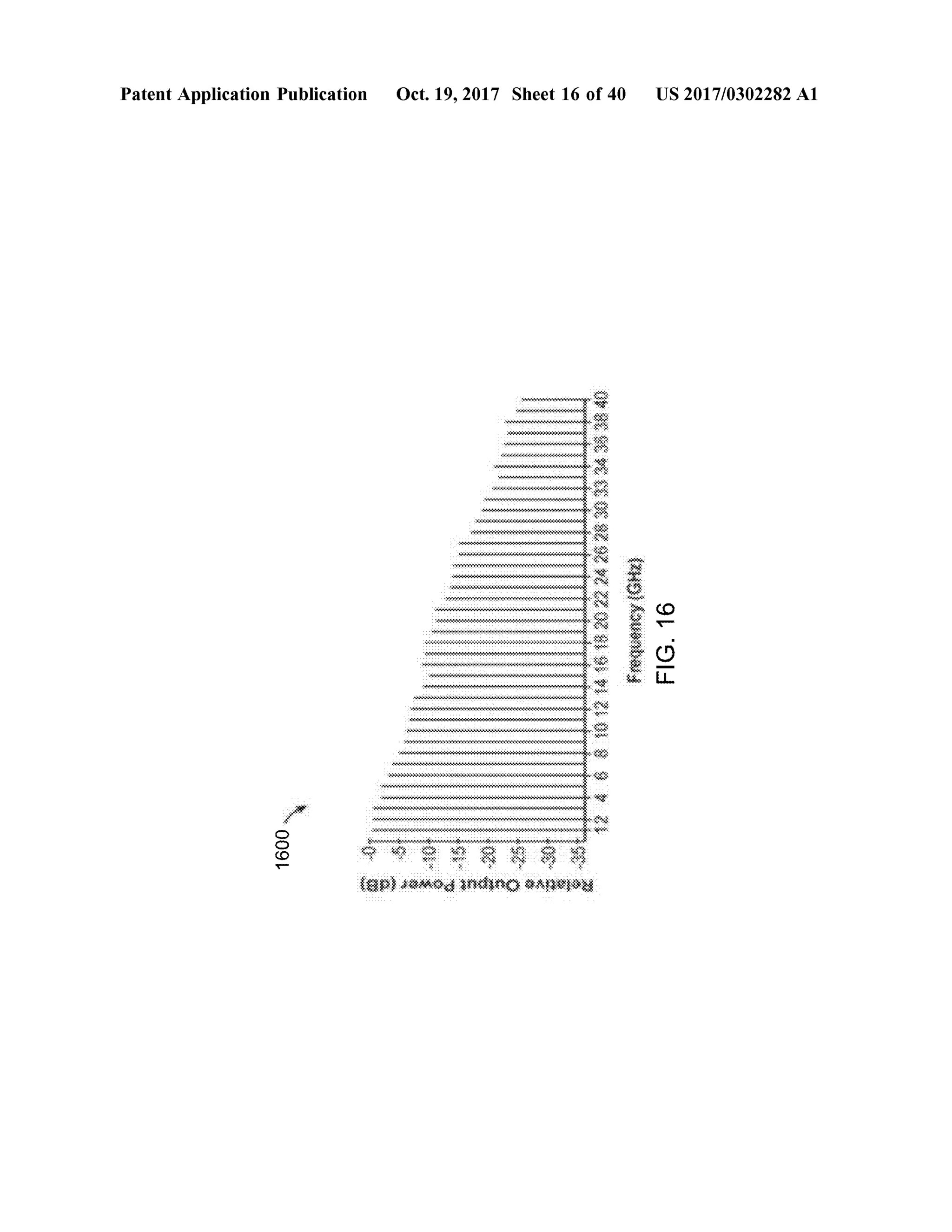
[0084] FIG . 16 illustrates an example output of a comb
generator in the frequency domain ;
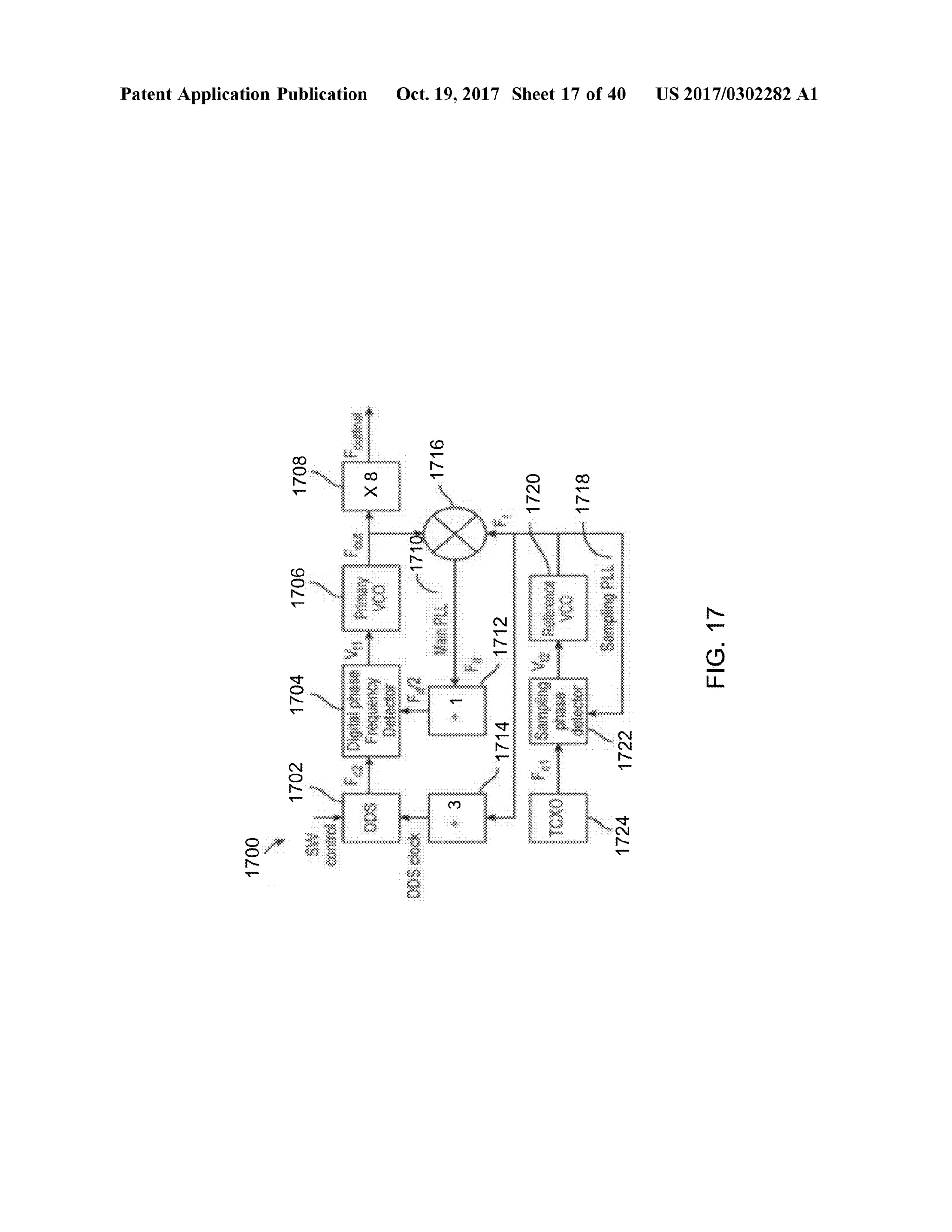
[0085] FIG . 17 illustrates a block diagram of an ultra -low
phase noise frequency synthesizer as suggested in a first
embodiment;
[0086] FIG . 18 illustrates a block diagram ofan ultra-low
phase noise frequency synthesizer as suggested in a second
embodiment;
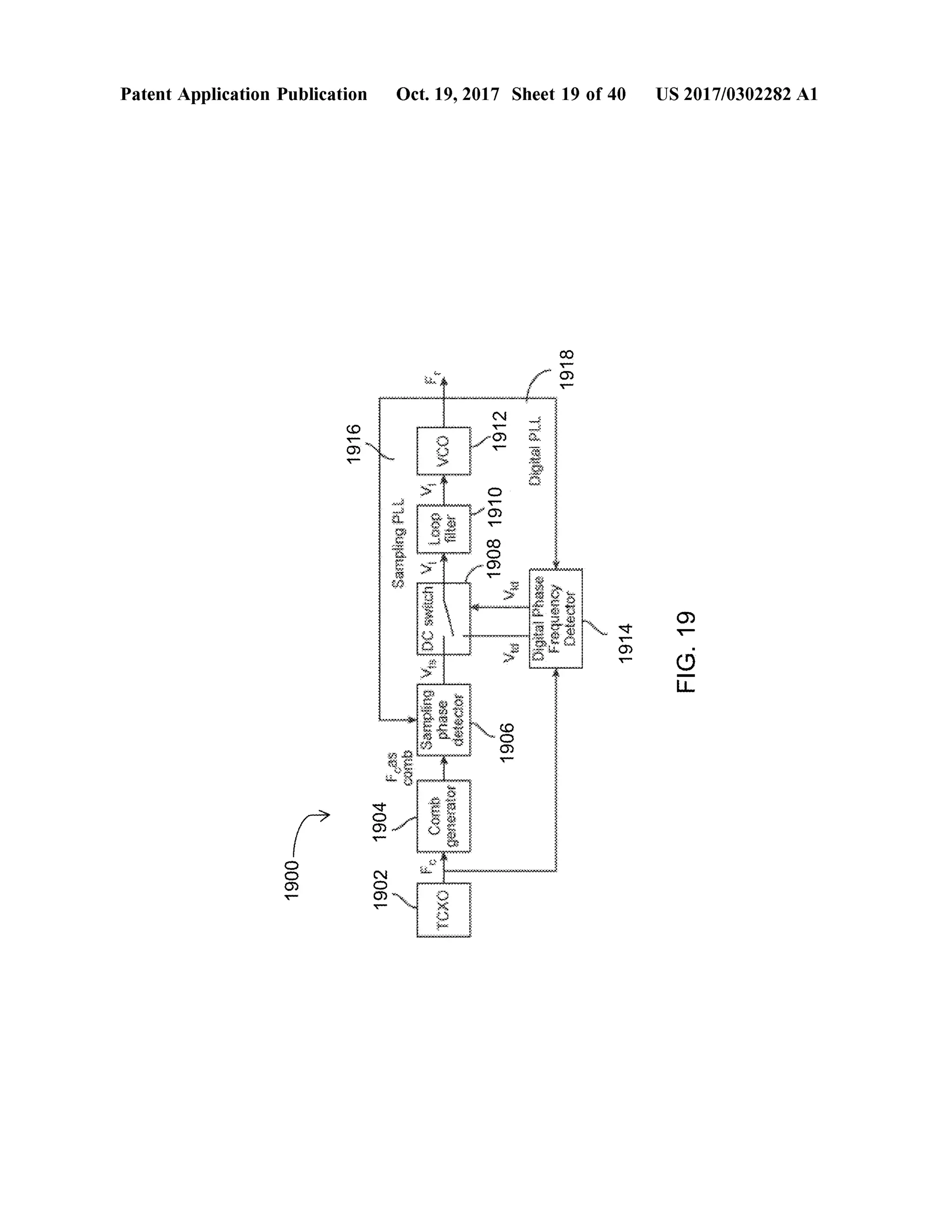
[0087] FIG . 19 illustrates ablock diagram ofthesampling
PLL system ;
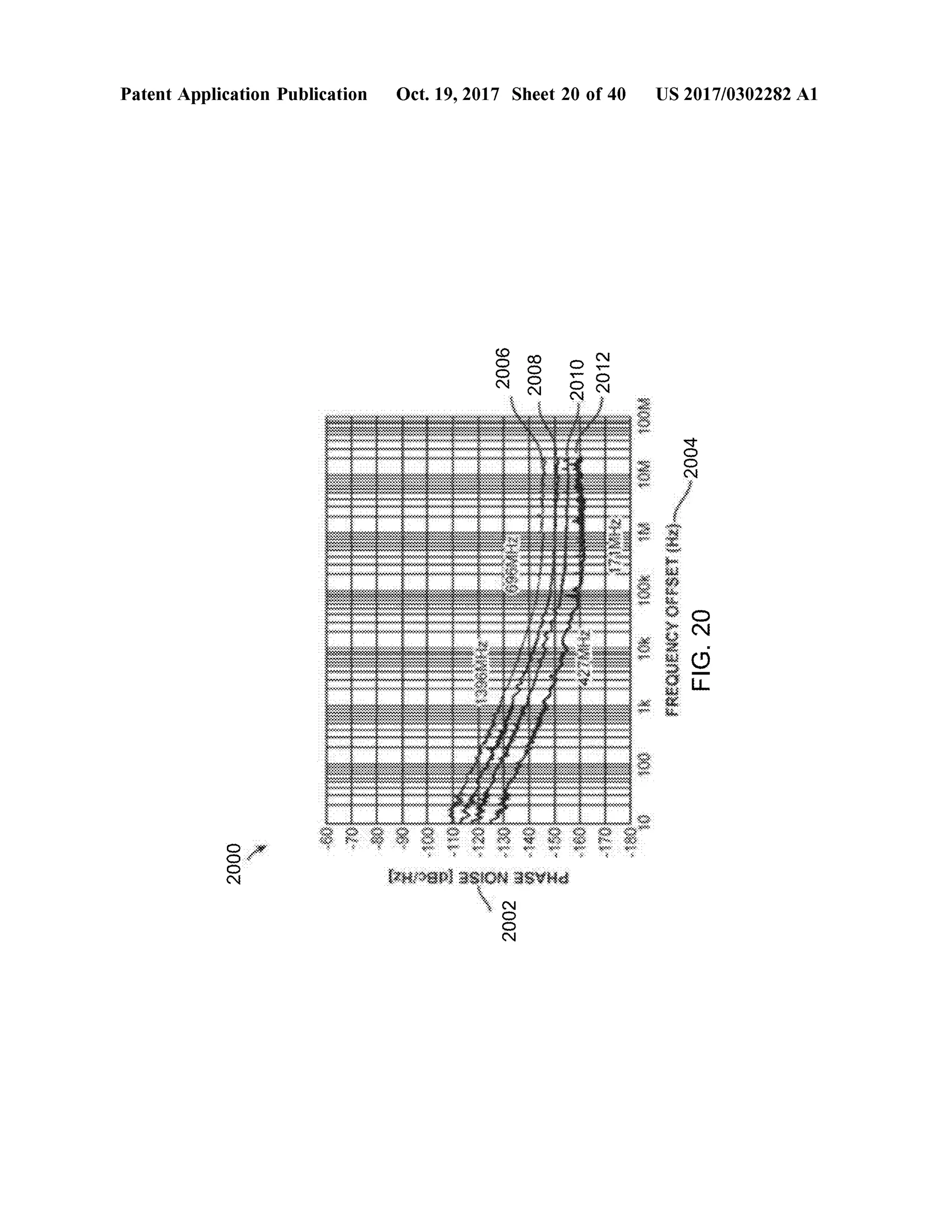
[0088] FIG . 20 illustrates a phase noise simulation plot
contributed by a DDS chip in accordance with the first
embodimentofthe present disclosure;
[0089] FIG . 21 illustrates a phase noise simulation plot
contributed by a main PLL in accordance with the first
embodimentof the present disclosure;
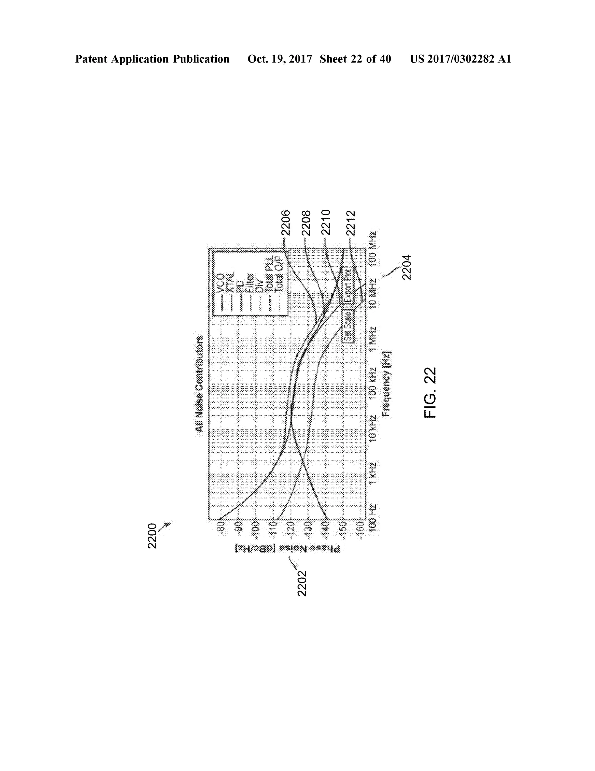
[0090] FIG . 22 illustrates a phase noise simulation plot
contributed by a reference sampling PLL having the TCXO
clock (or any other reference Clock ) generating input fre
quencies of 100 MHz in accordance with the first embodi
ment of the present disclosure;
[0091] FIG . 23 illustrates a phase noise simulation plot
contributed by areference sampling PLL having the TCXO
clock (or any other reference Clock ) generating input fre
quencies of250 MHz in accordance with the first embodi
mentof the present disclosure;
[0092] FIG . 24 illustrates a phase noise simulation plot
contributed by a main PLL in accordance with the second
embodiment of the present disclosure;
DETAILED DESCRIPTION
[0103] As used throughout this application, the word
“may” is used in a permissive sense (i.e., meaning having
the potential to ), rather than the mandatory sense (i.e.,
meaningmust).Similarly, thewords“ include”,“ including”,
and “ includes” mean includingbutnot limited to .
[0104] The phrases “ at least one”, “one or more”, and
" and/or” are open-ended expressions thatare both conjunc
tive and disjunctive in operation. For example, each of the
expressions “atleast one of A, B and C ”, “atleast one of A ,
B, or C ”,“ one ormore of A , B ,and C ”,“oneormore of A ,
B , or C ” and “ A , B , and/or C ” means A alone, B alone, C
alone,A and B together,A and C together, B and C together,
or A , B and C together.
10105 ] The term “ a” or “ an" entity refers to one ormore
ofthat entity.Assuch, theterms“ a” (or“ an” ), “one ormore”
and " at least one” can be used interchangeably herein. It is
also to be noted that the terms “ comprising”, “ including”,
and “having" can be used interchangeably.
101061 The term “automatic” and variations thereof, as
usedherein, refers to any process or operation donewithout
material human input when the process or operation is
performed .However, a process or operation can be auto
matic, even though performance ofthe process or operation
uses material or immaterial human input, if the input is
received before performance of the process or operation .
Human input is deemed to bematerial if such input influ
ences how the process or operation will be performed.
Human inputthat consents to theperformance ofthe process
or operation is not deemed to be “material” .
0107] The presentdisclosure includes implementation of
an upgraded Radar unitby incorporatingan ultra-low phase
noise frequency synthesizer to make the radar functioning
effective by transmitting radio signals with much lower](https://image.slidesharecdn.com/us20170302282a1-200617153345/75/Radar-target-detection-system-for-autonomous-vehicles-with-ultra-low-phase-noise-frequency-synthesizer-48-2048.jpg)
![US 2017/0302282 A1 Oct. 19,2017
phase noise than what is found in traditionalRadar systems
on the transmit side.On the receive side ofthe Radar system
theultra-low phase noise synthesizer addsonly a very small
amountofphase noise to the signal.More specifically, in an
embodiment, the upgraded radar unit generates a very low
amount of phase noise and thusminimizing the impact of
phase noise on the transmitted and the received signal. The
Radar unitmay include a Synthetic Aperture Radar, or any
other kind of Radar, for determining information corre
sponding to targets. Further, the present disclosure may
utilizemodulated signalsuch as FrequencyModulated Con
tinuous Wave (FMCW ) ofany type orany othermodulated
signalfor the RadarUnit.Asmentioned above FMCW based
Radar are advantageousin termsofpower saving Further, in
FMCW based Radar unit, various factors such as distance
and velocitiesmay be determined based on frequency dif
ferences from the instantaneous transmitted signal rather
than travel time. In most cases FMCW Radar signals are
processed with the help of FFT utilizing signalprocessing
windows and pulse compression algorithms. While these
methods are good, phase noise of the system still remains
important since it is a statistical phenomenon thatmay be
measured and calculated as an average, but instantaneous
value thereof cannot be determined, thus it cannot bemiti
gated easily with existingalgorithms.However,its influence
on system performance will drastically be reduced with the
collaboration of ultra-low phase noise frequency synthe
sizer. As a result, the overall system capability of accuracy
and target detection willbe vastly improved
[0108] FIG . 1 illustrates a general block diagram of a
negative feedback system 100. The negative feedback sys
tem 100 has an input R and an output C , a summer/
comparator 102, a forward path function G 104 and a
feedback path function H 106 . The summer/comparator 102
compares the input R with a sample B of the output C fed
back through function H 106 , to produce an error signal E
that is relative to the difference between the input R and the
feedback sample B . This error signal E is fed to the main
element G function 104 in the forward path . If the output
signal C tends to drift upwards, the error signal E pushes it
back downwards and vice versa. Thus, the negative feed
back system 100 stabilizes the output signal C . Thenegative
feedback system 100 finds applicationsin many systemsfor
stabilizing frequency, outputpower, and many other func
tions.
[0109] FIG . 2 illustrates a general block diagram of a
standard Phase Lock Loop (PLL ) 200. The PLL 200 is a
frequency feedback system comprising a reference clock
202, a digitalphase/frequency detector (PFD ) 204, a loop
filter 206, a Voltage Controlled Oscillator (VCO ) 208, and a
frequency divider 210.
[0110] The VCO 208 is the main output block in the
forwardpath,and is tuned to produce a frequency as setby
a tuned circuit. The VCO 208 has a frequency output Fout
that can be changedby a control voltage Vtover a pre-set
range of frequencies.
10111] Thephase detector 204 is a comparator forboth the
clock inputFclock and the feedback sample from the output
Fout divided by divider N 210. The phase detector 204
compares the two input frequencies Fclock and Fout/N .
When the two input frequencies are not equal, the device
204 acts as a frequency discriminator and produces either a
negativeorpositive voltage, depending on thepolarity ofthe
frequency difference between the two inputs.When the two
inputfrequenciesarethe deviceproducesan errorvoltage Vt
relative to the phase difference between the two equal
frequencies.
[0112] The loop filter 206 filters and integrates the error
signal produced bythe phase detector 204 and feeds it to the
VCO 208. The loop filter 206 is usually based on passive
components like resistors and capacitors, but also in some
cases it is a combination of active devices like operational
amplifier and passive components.
[0113] The reference clock 202 is in general a low fre
quency crystal oscillator signal source that feeds Fclock to
the phase detector 204, and to which theoutputsignalFout
is “ locked”. Thereference clock 202 is setatsome frequency
for example a standard frequency 10 MHz. The locking
“mechanism ” transfers someofthequalities of thereference
clock 202 to themain output signal Fout. Itsmain features
usually are: a) frequency stability over temperaturegen
erally in the range of 0.1-5 ppm (parts per million), b )
accuracy - Can be tuned to very high accuracy, c ) very low
phase noise - Its phase noise is transferred to the output
signalmultiplied by theratio of20*LOG (N ) where N is the
ratio between theoutputfrequency and theclock frequency
applied to the phase detector 204.
[0114] The frequency divider 210 is based on digital
devices like gates and flip -flops, through which the input
frequency Fout is divided by a number N to produce Fout/N
which is fed to theother inputofthe phase detector 204. This
number N issoftware controllable. The control signal comes
usually from a micro controller or from a PC or from
anywhere that basically will send software control to the
frequency divider 210 to change the division number N . The
target of the division number N is to enable the output
frequency of the frequency divider 210 to be equal to the
clock frequency ofthe reference clock 202.
[0115 ]. The entire operational procedures of a standard
Phase Lock Loop (PLL ) 200 is as follows: If an inputclock
signal Fclock is applied, usually by a reference clock 202,
the phase detector 204 comparesthe phase and frequency of
the input signalFclock with thatoftheVCO 208 divided by
N , and generates an error voltage Vt that is related to the
difference in the two signals. The error voltage Vt is then
filtered and applied to the controlof the VCO 208, thereby
varying the VCO 208 frequency in a direction that reduces
the frequency differencebetween thetwo signals.When the
frequencies of the two signals become sufficiently close, the
feedback nature ofthe system causes the system to lock with
the incoming signal.Once in lock the VCO 208 frequency
dividedby N is identicalwith the inputsignalFclock,except
for a finite phase difference which is necessary to generate
the corrective error voltage Vt to shift the VCO 208 fre
quency to the input signal frequency Fclock, thus keeping
the system in lock .
[0116 ] Any time, the division number N is changed,say
for example by 1, the output frequency Fout jumps exactly
bya step. In an example,if the reference clock 202 generates
a frequency 1 MHz, then every time the division number N
changesby stepsof 1, theoutputfrequency Fout changesby
equalsteps of 1 MHz.
10117]. Like all negative feedback systems, the PLL 200
has a loop bandwidth setby the componentparameters and
the loop filter 206. In other words, the PLL 200 is a
sophisticated frequency multiplier with a built-in narrow
band, automatically tuned band-pass filter as the output
frequency Foutis basically Fclockmultiplied by thenumber](https://image.slidesharecdn.com/us20170302282a1-200617153345/75/Radar-target-detection-system-for-autonomous-vehicles-with-ultra-low-phase-noise-frequency-synthesizer-49-2048.jpg)
![US 2017/0302282 A1 Oct.19,2017
een
N . The loop bandwidth is also responsible directly forhow
fast the output frequency ofPLL 200 may change between
different frequencies. The PLL 200 is a device where the
VCO 208 is locked to a single clock reference signalwhich
is very low butalso very clean and very stable and theoutput
frequency can be changed by equivalent stepsby controlling
the frequency divider 210 in the feedback loop.
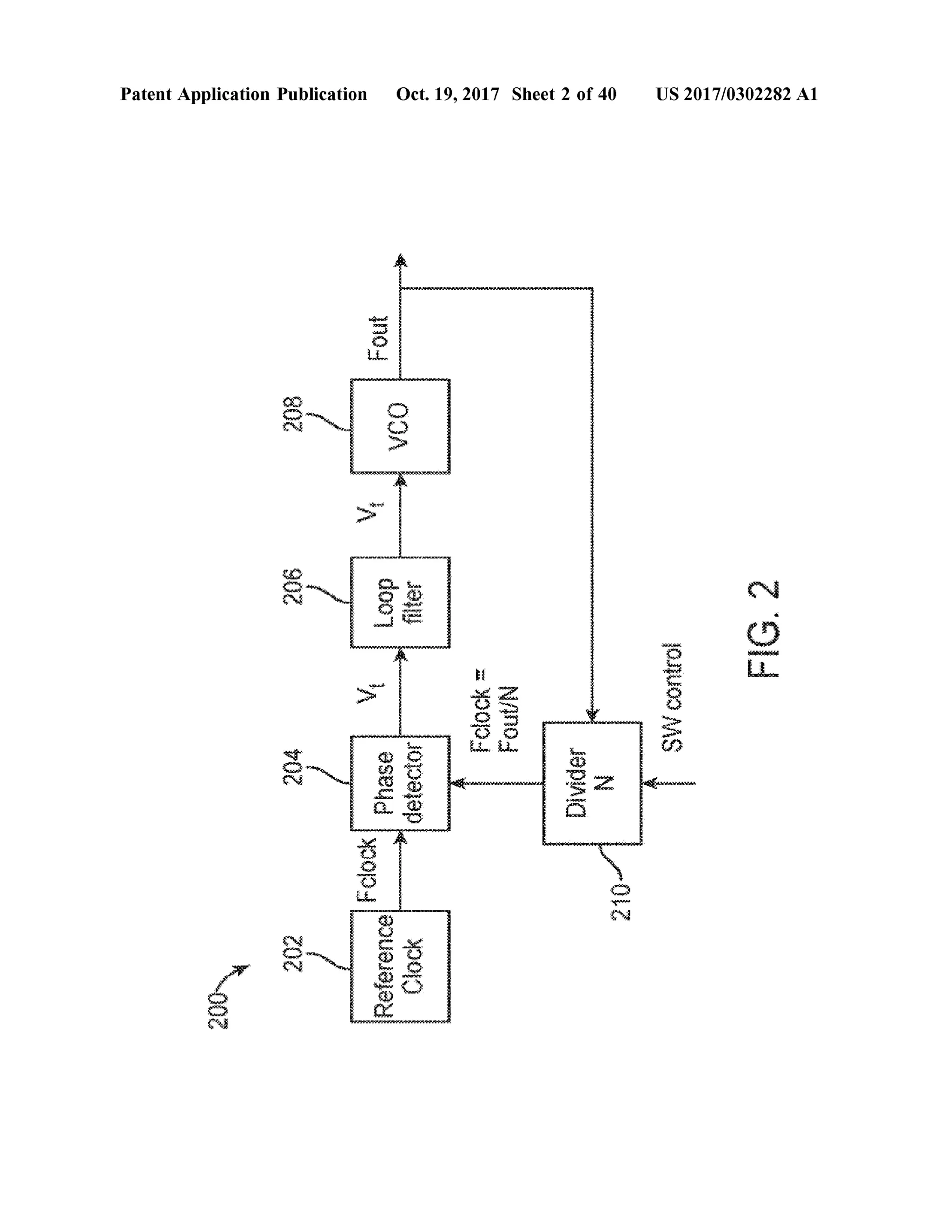
[0118] FIG . 3 illustrates a simplified drawing of a digital
phase/frequency detector 204. A phase detector or phase
comparator is a frequency mixer, analog multiplier or logic
circuit that generates a voltage signalwhich represents the
difference in phase between two signal inputs. It is an
essential element of the phase-locked loop (PLL ). A spe
cialized variant that additionally detects frequency is
referred as Phase Frequency Detector (PFD ). A phase
frequency detector is an asynchronous sequential logic cir-
cuit which determines which of the two signals has a
zero -crossing earlier or more often .When used in a PLL
application, lock can be achieved even when it is off
frequency. Such a detector has the advantage of producing
an outputeven when the two signalsbeing compared differ
not only in phasebut in frequency.
[0119] The phase/frequency detector 204 compares two
input frequencies Fclock and Fout/N . When the two input
frequencies arenot equal, it acts as a frequency detectorand
produces one or zeros to produce a voltage control Vt that
pushes corresponding VCO 208 in the direction of the
reference. In other words, if the VCO 208 is above the
reference then the voltage control Vt is high to push the
VCO 208 down and vice versa. When the two input fre
quencies are the same and a frequency lock is achieved, the
phase detector 204 acts as a phase detector and compares the
two phases, and continues to produce an error voltage to
control the frequency and phase of the output device.
[0120] FIG . 4 illustrates an example ofan active filter as
applied to a general PLL 400. The kind of loop filter i.e.
passive filter or active filter can be chosen on the basis of
specific requirement. A passive loop filter is based on
resistors and capacitors only, while an active loop filter is
based on an amplifier and a capacitor-resistor network in the
feedback system . A passive filter ispreferred in caseswhere,
a reference PLL is of a single frequency and will need only
a single voltage in order to stay in that single frequency. The
other reasons being simplicity, cost and most advanta
geously no addition of noise, as active devices tend to add
additional noise in the system . However, active filters find
more acceptances because ofthepossibility ofamplification
of the input signal. Amplification is made possible by an
operational amplifier employed in the active filter.
[0121] Theloop filter 206,ofFIG . 2, is an active filter that
includes an operational amplifier 402 and a capacitor-resis
tor network 404 in the feedback loop. In some instances,the
phase detector 204 ofthe PLL 200may produce voltage up
to 5 volts but the corresponding VCO 208 may need a
voltage of above 5 volts,say, for example,up to 18 volts in
order to reach its complete range, so the active filter 206
facilitates not only filtering butalso provides the capability
to go to higher voltages.
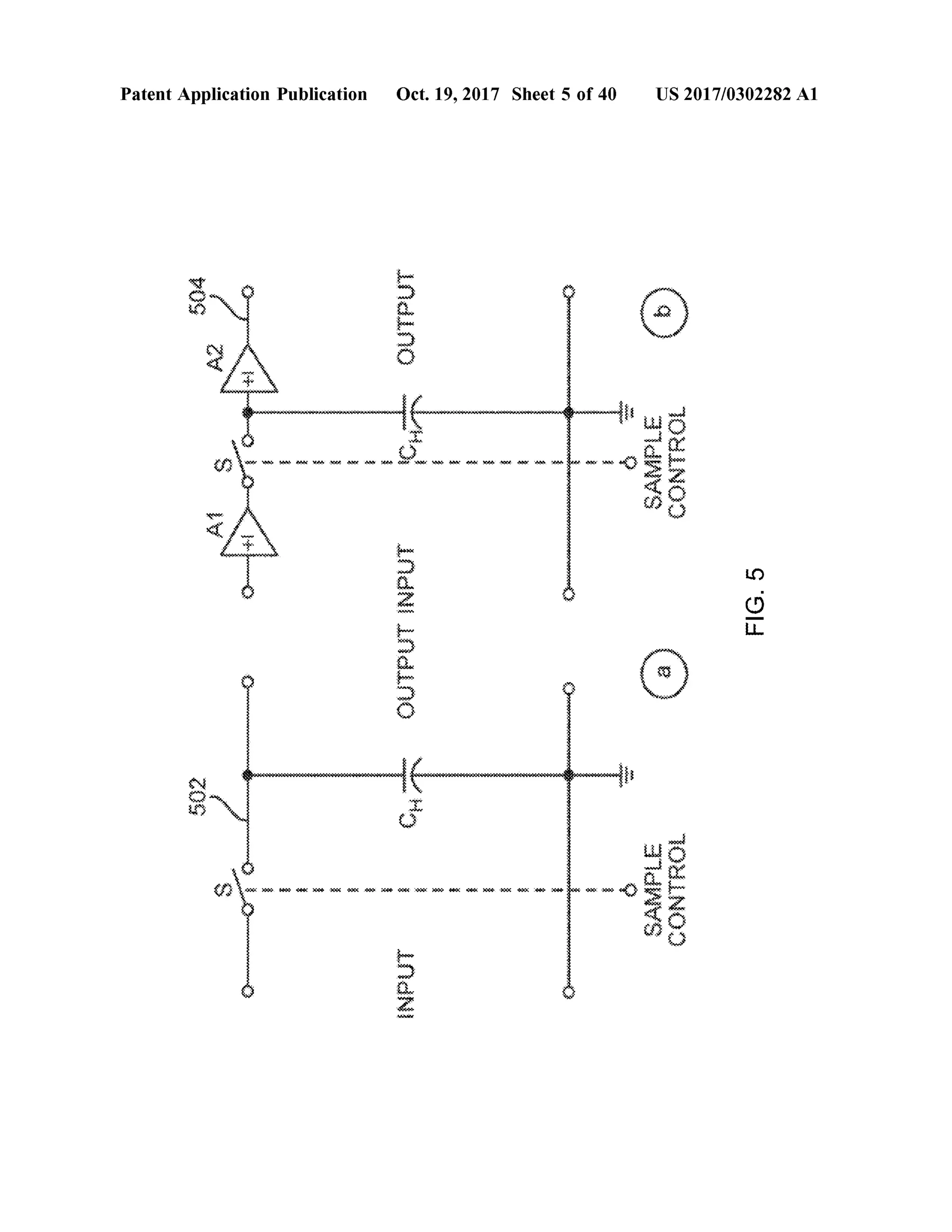
[0122] FIG . 5 illustrates theprinciple of sample-and-hold
mechanism 500. The first sample and hold circuit 502
includes a switch S and a hold capacitor CH . The operation
of the switch S is controlled by the sample control.When the
switch S is closed, a voltage sample ofthe input frequency
is sampled and when the switch is opened, the voltage
sample is held on the hold capacitor CH .
[0123] The second sample and hold circuit 504 includes
two buffers A1 and A2 with unity gain for isolation pur
poses, in addition to the switch S and thehold capacitor CH .
The buffer A2 is preferably an electronic buffer, so that the
hold capacitor CH does not discharge parasitically between
consecutive samples. In other words, thehold capacitorCH
holds the voltage between samples.
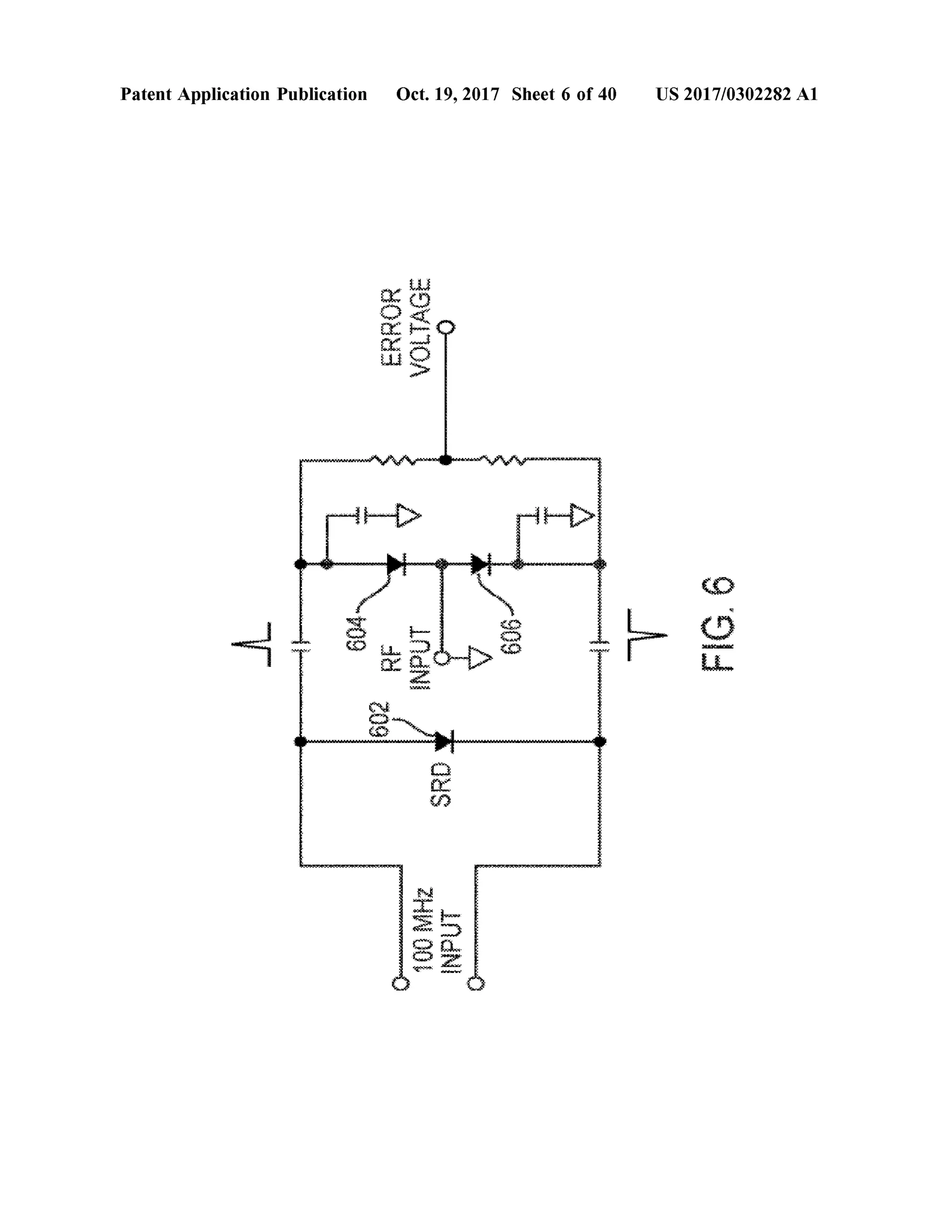
[0124] FIG . 6 illustrates an example ofpractical imple
mentation of a comb generator and sampling phase detector.
The schematic shows a Step Recovery Diode (SRD ) as
comb generator feeding the dual schottky diode thatacts as
phase detector. The implementation circuit 600 including a
Step Recovery Diode (SRD) 602 as a comb generator and
the dual schottky diodes 604 and 606 as a phase detector.
10125 ] The input to the circuit 600 in this example is a
clock inputof100MHz sinewave. The SRD 602 is a special
device that turns the 100 MHz sinewave input into a very
narrow pulse train of the samefrequency, so it acts as a comb
generator. The two schottkydiodes 604,606 actas switches
and act as sampling switches. TheRF voltage (outputfrom
corresponding VCO) to be sampled is connected to a point
between the two diodes604 and 606. The SRD 602 creates
an outputofpositive and negative pulses. The positive and
negative pulsesact as control signals to the diodes 604 and
606 thatact like switches. The sampled voltage output is an
errorDC voltage which is created by sampling the RF input
through the dual schottky diodes 604 and 606. The outputof
the RF signal is sampled whenever the diodes 604 and606
are opened by thenarrow pulses coming from the SRD 602.
The voltage sample is held on the capacitors C followingthe
diodes 604 and 606.
[0126 ] FIG . 7 illustrates a schematic ofthe comb genera
tor and sampling phase detector with a clock pre-amplifier
and two DC buffers following the phase detector. The
voltage samples are held on two very small capacitors
(which are basically the input capacitance of the voltage
buffers,no need for externalcapacitors)onboth sidesofthe
dual diode pair, so as not to enable the whole capacitor to
discharge parasitically between the samples. These capaci
tors are buffered by a couple ofultra-low input bias current
buffers to prevent discharge between samples. The two
voltages are summed,fed to a loop filter,whereby theclean
Vt is fed to the VCO to control the frequency.
[0127] This implementation of sampling phase detector
creates an analog phase detector,very similar to amixer. The
analog sampling phasedetectorhas a certain defined locking
space or locking distance, and it does not lock from any
frequency difference like thephase/frequency digital detec
tor. It has some locking range and only within that locking
range, the VCO locks by itself on the reference. In a
sampling PLL, the VCO does not lock on the reference,but
on the Nth harmonic ofthe reference. In other words, one
can lock a 9GHzon the 90th harmonic ofthe 100Megahertz
clock. This is done asthe input frequency is sampled every
100 cycles, not every cycle.
10128] This type of product may contain some “search
mechanism ” to help lock the PLL. The most common one
involves a positive feedback on the loop filter itself.While
the loop is not locked , the loop filter acts as a very low
frequency oscillator that drives the VCO back and forth
across the frequency range. When it passes close enough to
theharmonic ofthe clock, it will lock and stay locked. A nice](https://image.slidesharecdn.com/us20170302282a1-200617153345/75/Radar-target-detection-system-for-autonomous-vehicles-with-ultra-low-phase-noise-frequency-synthesizer-50-2048.jpg)
![US 2017/0302282 A1 Oct.19,2017
feature of this mechanism is that it turnsoff automatically
when the loop locks. This happensbecause ofthe nature of
the loop as a negative feedback system .
[0129] However, this type of search mechanism suffers
from many problems,its operation is subjectto temperature
changes and itmakes this product difficult to produce, tune
and sellsuccessfully.
[0130] FIG . 8 illustrates a phase noise plot 800 of an
example free running Voltage ControlOscillator (VCO ) in
the frequency domain (spectrum analyzer), withoutbeing
locked in a PLL .Assaid before, Phase noise is a key element
in many RF and radio communications systems as it can
significantly affecttheperformance ofsystems. Phase noise
is the frequency domain representation of rapid , short-term ,
random fluctuations in the phase of a waveform , caused by
time domain instabilities also referred to as “ jitter" .
[0131] For example, in frequency domain, where the
scales are amplitude vs. frequency, ideally a frequency of
100 MHzmay look like a single line staying at exactly 100
MHz.However, practically with modern equipment in the
laboratory, amplitude vs frequency may not look like a
single line butitwill look like a single linewith a “skirt” 802
which goeswider and wideraswegodown. The phasenoise
plot800 looks like the skirt 802 on the left and the rightof
the exact desired frequency fo. The quality,height,width of
the skirt 802 determineshow the phase noise may affect the
system or theperformance of the system . So, it is desirable
to minimize phase noise as much aspossible is to improve
the system performance.
[0132] Phase noise is anotherterm to describeshort-term
frequency stability. The signal generated by a frequency
source is never practically “clean” . Its frequency is never
absolutely stable at the desired value. Ithas “Phase Noise”
which is frequency shifting, i.e. small frequency shifts at
different rates and different amplitudes of the main fre
quency. It changes around the center set frequency fo at
different rates and amplitudes. In time domain, the phase
noise may be referred to as jitter. Long term frequency
stability is drift of the center frequency over time or over
temperature.
[0133] FIG . 9 illustrates a phase noise plot 900 of an
example Voltage ControlOscillator (VCO ) in the frequency
domain (spectrum analyzer), compensated by being locked
in a PLL.
[0134] Theupperline 904 is the free running VCO phase
noise,before it is locked in a PLL, and the lower line 902 is
the shaped VCO phase noise. In the PLL, the principle of
locking the VCO to a reference frequency attenuates the
phase noise of the VCO, in an amount related to the loop
bandwidth. Outside the loop bandwidth, the VCO noise
remains almost same as the phase noise without the PLL ,
while inside loop bandwidth it is attenuatedmore andmore
asoffset frequency from themain carrier is reduced.At very
high frequency, i.e. above the loop bandwidth , the locking
almosthasno effect, as the phase detector correction signal
is not fast enough to reach the VCO for very fast changes or
very fast disturbances.However, inside the loopbandwidth
or at low frequencies, the compensated phase noise of the
VCO is much lower than that of the free running VCO . All
the frequencies that is close to the centerofthe frequency fo
are easy to detect and compensate .
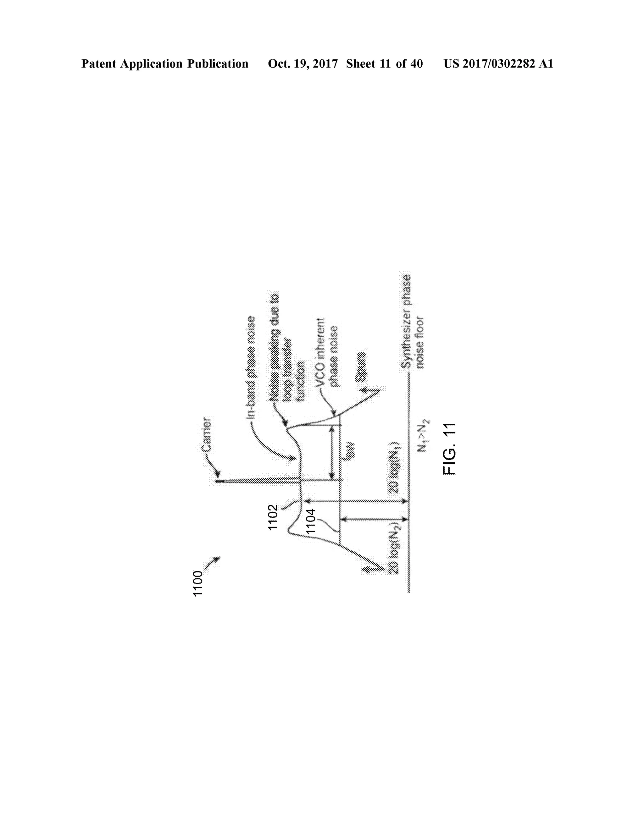
[0135] FIG . 10 illustratestwo plots 1000: (a ) a simulation
of phase noise of an example PLL , and (b ) an actual
measurement. FIG . 10(a ) illustrates a simulation graph of
phasenoise ofan example PLL. The simulation graph shows
the overall phase noise ofthe example PLL and includes the
contribution of all the components that contribute to the
phase noise. The simulation graph illustrates first, second
and third regions 1002, 1004 and 1006 ofthe phase noise.
The first region 1002 which is very close to the carrier
depicts a steep line which basically comes from the refer
ence clock such as the Temperature Controlled Crystal
Oscillator (TCXO , or any other reference clock device). The
first region depicts thenoise ofthe TCXO,multiplied by 20
logN , where N is the ratio ofoutput frequency to the clock
frequency. The second region 1004 depictsa flatphase noise
which isbasically the noisefloorofthedigitalphase detector
multiplied by the same ratio of 20 logN . The third region
1006 depicts a steep line which is the inherent VCO phase
noise not affected by the loop bandwidth and locking phe
nomenon. The dashed line 1008 depicts the VCO "cor
rected” phase noise inside loop bandwidth .Below the flat
area, the compensated VCO phase noise does notaffect the
overall result because it is way below the noise floor of the
phase detectormultiplied by that ratio . The actualmeasure
ment of phase noise of an example PLL is illustrated in FIG .
10 (! ). One can see clearly the similarity between the two
curves.
[0136] FIG . 10 illustrates a phase noise plot 1100 of a
closed loop PLL , showing clearly the effect of the phase
detector multiplication number 20*LOG (N ) within loop
bandwidth .The phase noise plot 800 illustrates phase noises
on both sides ofthe carrier frequency fo, where the left side
is a mirrored image of the right side. The phase noises on
both sides ofthe carrier fo looks like it is passing through a
band-pass filter.
[0137] As illustrated, on both sides, the in-band phase
noise inside the loop bandwidth is flat in shape and is equal
to the phase detector and/or the reference clock noise
multiplied by 20 logN .Atthepointof the loop bandwidth ,
thephase noise goes up before going down again . This is due
to addition of 3 dB due to a combination ofphase noise of
the free running VCO and the phase detector. The upper
straight line 1102 depicts a phase noise contributed by the
phase detector atN1and the lower straightline 1104 depicts
a phase noise contributed by the phase detector atN2. It can
be seen that, there is difference in phase noise in the flatarea,
due to two different “ N ” numbers. The phase detector
contributes a higher in-band phase noise at a higher value of
N .
[0138] Thus, in order to achieve low phase noise, it is
essential to : a ) choose components such as phase detector
and reference clock with the lowest inherent phase noise
possible, and b ) lower the ratio number N as much as
possible.
[0139] FIG . 11 illustrates plot 12902200 ofmeasurement
terms of phase noise in 1 Hz bandwidth at a Af offset
frequency from the carrier. The phase noise expression is
usually in dBc, i.e. dB relative to the carrier c power level
Ps, in otherwordshow low it is compared to the carrier per
Hz, in abandwidth of 1 Hz. That isbasically theterm that
is used for phase noise,dBc perHertz (dBc/Hz)at a certain
Af from the carrier.
[0140] As an example forthemeasurementmethod, sup
pose AF is 10 KHz, the phase noise power level Pss is
measured at the level of - 70 dBm on the spectrum analyzer,
and the carrier power level Ps is measured at thelevel of 10
dBm , the ratio between the Ps 10 dBm and the PssB - 70](https://image.slidesharecdn.com/us20170302282a1-200617153345/75/Radar-target-detection-system-for-autonomous-vehicles-with-ultra-low-phase-noise-frequency-synthesizer-51-2048.jpg)
![US 2017/0302282 A1 Oct. 19,2017
dBm at 10 KHz from the carrier is therefore 80 dB , so the
phase noise at 10 KHzoffset from carrier and is -80 dBc/Hz.
10141] For many systems, the important parameter to
evaluate performance is not the phase noise measured at a
single frequency offset from the carrier,but the integrated
phase noise from one offset frequency to another one.
Following are four different equations and terms to define
integrated phase noise:
fuper
Sphi(S)=(1.0).12.juhudi
Sulf)= V2.5Lf).f?df
8,(8)=(Computer )J
Where the first equation describes single sideband phase
noise [dB ]
[0142] The 2nd equation describes the spectral density of
phase modulation, also known as RMS phase error (de
grees)
[0143] The 3rd equation describes the spectral density of
frequency fluctuations, also known as RMS frequency
error or residualFM (Hz)
[0144] The 4th equation describesthe spectral density of
fractional frequency fluctuations
[0145] For example, the first equation defines the Phase
Noise in dBc. It can be translated by the 2nd equation to
degrees (relevant in respect of learning modulation
schemes).Asper further equations, the phase noise can also
be translated in terms ofHz and timedomain phase jitter
seconds.
[0146] FIG . 13 illustrates a generalblock diagram 1300 of
an example dual loop PLL. Themain targetof thedual loop
design is to reduce themultiplication number N in themain
of the mixer 1312 and feed to the second phase detector
1308. ThevalueofN1 is setasminimal,as theoutput from
the mixer 1312 is at a much lower frequency than original
frequency range F1 to F2.
[0152] To give an example: a) Suppose Fc= 1 MHz, b)
Suppose F1 to F2= 10,000 to 11,000 MHz. Then N = 10,000
to 11,000.Now If Fr= 9000 MHz, then ((F1-F2)-Fr)= 1000
to 1900 MHz. Then N1= 1000 to 1900. Thus,the value of N
is reduced from 11,000 to 1900. In dB , it is a ratio of 15 dB .
Thismeans,thatthe phase noise is reduced by a factorof 15
dB .
[0153] Thedisadvantage ofthe example dualloop design
is thatwhile nicely reducing the number N in themain PLL,
the reference PLL, containing a digital phase/frequency
detectorbecomes themain factor contributing to the overall
outputphase noise.
[0154] FIG . 14 illustrates a generalblock diagram 1400of
an example sampling PLL . Thesampling PLL 1400 includes
a TCXO 1402, a comb generator 1404, a sampling phase
detector 1406 , a loop filter 1408, and a VCO 1410. The
sampling PLL 1400 doesnot include digitalphase/frequency
detector and frequency divider. Thus,no digital noise floor
is generated thatcan bemultiplied andaffect performanceof
the system .
[0155] The TCXO 1402 feeds the clock signal Fclock to
the comb generator 1404. The comb generator 1404 is a
device thatchanges the inputsine wave signal at frequency
Fclock to an output signal ofvery narrow pulses at the same
frequency as the input sine wave signal.
[0156] The pulse output from the comb generator 1404 is
used as a control signalto thesamplingphase detector 1406.
The sampling phase detector 1406 receives an RF signalof
frequency Fout from the VCO 1410, and includes two
diodesactingas switches to sample the RF signalby opening
and closing the diodesbased on the narrow pulses from the
comb generator 1404. The sampled voltage Vtproduced is
“held ” on capacitors and buffered until the next sample
period. The voltage samples are always at the same level,
thus a DC voltage Vt is generated by the sampling phase
detector 1406 . The loop filter 1408 cleans and filters theDC
voltage Vt, and provides it to the VCO 1410 to control the
VCO frequency Fout. Fout= Fclock *N , where N is the Nth
spectralharmonic line in the “comb" spectrum .
[0157] FIG .15illustratesblock diagram 1500 depictshow
the impulse or“ comb” generator 1404 changes a wave shape
of a signal from sine wave 1502 to narrow pulses 1504. A
frequency source 1506 generates the input sine wave 1502
of frequency F1 and time period T1.
f0158]. The comb generator 1404 turns the input sinewave
1502 to a series ofvery narrow pulses 1504 with same time
period T1,and a pulse bandwidth as tp in the timedomain.
Forexample, if the frequency ofinput sinewave 1502 is 100
MHz, then the impulse train generator 1508 generates a
series of very sharp narrow pulses 1504 of the same fre
quency.
[0159] FIG . 16 illustrates an example output 1600 of a
comb generator 1404 in the frequency domain. In the
frequency domain (spectrum analyzer screen ), the output
1600 ofthe comb generator 1404 looks like a “comb”, i.e.
a row oflinesextending up to very high frequency. In theory,
if the bandwidth of the clock pulse is infinitesimal, the row
of lines appearwith equalamplitude to infinity. The output
1600 looks like a series of lines, with the spacing between
PLL.
[0147] The dual loop PLL 1300 includes an upper PLL
1302, referred to as a main PLL 1302, and a lower PLL
1304, referred to as a reference PLL 1304, a TCXO 1306
operatingas a master clock, feeding a clock signalFc to both
the primary PLL 1302 and the reference PLL 1304.
[0148] The reference PLL 1304 includes a first phase
detector 1314, and a single frequency first VCO 1316 that
operates at a reference frequency Fr. The reference fre
quency Fris fed to a first input of a down convert mixer
1312.
[0149] Themain PLL 1302 includes a secondphase detec
tor 1308 and a second VCO 1310 that generates an output
frequencyrange F1 to F2. A sampleofthe output frequency
rangeF1to F2 is fed to thesecond inputofthe down convert
mixer 1312 and mixed with a single reference frequency Fr.
The output from the down convertmixer 1312 is at a much
lower frequency (F1 to F2)-Fr. This lowered frequency is
fed back to the second phase detector 1308 through a
frequency divider 1318 of value N1.
[0150] Therefore: a ) Without the down convert mixer
1412: F1 to F2=NxFc, b) With the down convert mixer
1312: (F1 to F2)-Fr=N1xFc. As a result there is a reduction
in the number N : N1/N = ((F1 to F2)-Fr)/(F1 to F2).
10151] The N1 number is basically the division number
that the frequency divider 1318 will use to divide the output](https://image.slidesharecdn.com/us20170302282a1-200617153345/75/Radar-target-detection-system-for-autonomous-vehicles-with-ultra-low-phase-noise-frequency-synthesizer-52-2048.jpg)
![US 2017/0302282 A1 Oct. 19,2017
[0164] The down convertmixer 1716 receives atleast one
reference signal of frequencies Fr and at least one output
signal of frequency Fout and generates at least one inter
mediate signal of frequency Fif and forwards it towards a
second fixed frequency divider 1712. The second fixed
frequency divider 1712 generates at least one signal of
frequencies Fif/N1 by dividing the incoming at least one
signal of frequency Fif by a predefined factor. The second
fixed frequency divider 1712 forwards the generated at least
one signal of frequencies Fif/N1 towards the Digital Phase
Frequency Detector 1704. Theprimary VCO 1706 forwards
the atleastoneoutputsignalFouttowards a fixed frequency
multiplier 1708 to generate at least one final output signal
Fout final.
[0165] It is importantto notice that frequency divider 1712
is optional and themain PLL can operatewithout division of
Fif.
the lines sameas the initial frequency. In an example, if the
initial frequency is 1 GHz, the spectrum of lines is 1 GHz
apart.
[0160] FIG . 17 illustrates a block diagram 1700 of an
ultra-low phase noise frequency synthesizer as suggested in
a first embodiment. The ultra-low phase noise frequency
synthesizer 1700 includes two Phase Lock Loops (PLLs).
One is a main PLL 1710 and the other one is a reference PLL
1718. Themain PLL 1710 comprises of a high frequency
low noise DirectDigitalSynthesizer (DDS) 1702 to generate
at least one clock signal Fc2 ofvariable frequency range.
Thehigh frequency low noise DDS 1702 generates the at
least one clock signal Fc2 of variable frequency range by
taking input from at least one software controllable instruc
tionsandatleastoneDDS clock signal. The frequency ofthe
at least one clock signal Fc2 is always lower than the
frequency ofthe atleast oneDDS clock signal. The atleast
oneDDS clock signalis generated by a first fixed frequency
divider 1714. The high frequency low noise DDS 1702
forwards the generated at least one clock signal Fc2 of
variable frequency range towards a DigitalPhase Frequency
Detector 1704.
[0161] The Digital Phase Frequency Detector 1704 com
pares two signals coming from two directions and generates
atleastone signal.One signalis the at least one clock signal
Fc2 of variable frequency range generated by the high
frequency low noise DDS 1702. The second signal is atleast
one signal of frequency Fif/N1 generated by a second fixed
frequency divider 1712. The Digital Phase Frequency
Detector 1704 compares these two signals and generates at
least one first control voltage Vt1 and forwards it towards a
primary Voltage Control Oscillator (VCO ) 1706 . The pri
mary Voltage Control Oscillator (VCO ) 1706 generates at
leastone output signalof frequency Fout from the received
at least one first control voltage Vt1 . The main PLL 1710
further comprises a down convertmixer 1716.
[0162] The primary role ofthe reference PLL 1718 is to
help themain PLL 1710 in reducing the phase noise present
in the at least one output signal Fout. The reference PLL
1718 comprises a reference clock (for example a Tempera
ture Compensated Crystal Oscillator (TCXO )) 1724 to gen
erate at least one first clock signal of a fixed single frequency
Fc1. Further,thereference PPL comprises a sampling phase
detector 1722 (that includes the comb generator and the
sampling phase detector) to generate at least one second
control voltage Vt2 and a reference Voltage Control Oscil
lator (VCO) 1720.
[0163] One important thing to notice here is that unlike
other dual loop designs, the reference PLL 1718 uses the
sampling phase detector 1722.Thereference PLL 1718 does
not use any kind digital devices like the Digital Phase
Frequency Detector 1704,or the first fixed frequency divider
N1 1714.Simultaneously the reference clock 1724 present
in the sampling PLL 1718 is also a very low noise generating
device.Due to these reasons thecontribution of phase noise
from the reference PLL 1718 to themain PLL 1710becomes
close to negligible. Thereference Voltage ControlOscillator
(VCO ) 1720 generates atleast one reference signal Fr and
forwards it towards the down convert mixer 1716. The
reference PLL 1718 plays a major part in all relevant
communications and similar systemsby being part of vari
ous frequency synthesizers, and also as a standalone fre
quency source for all thesystemsofup and downconversion
processes in the same equipment.
[0166] To explain the above disclosed disclosureswith an
example let's say the reference clock 1724 generates the at
least one first clock signal of a fixed single frequency Fc1
100 MHz. The sampling phase detector 1722 generates the
second controlvoltage Vt2 by sampling the at least one first
clock signalof a fixed single frequency Fc1 100 MHz and
forwards the sampled values of the at least one first clock
signalofa fixed single frequency Fc1100MHz towardsthe
reference Voltage Control Oscillator (VCO ) 1720. The ref
erence Voltage ControlOscillator (VCO ) 1720 generates the
atleast one reference signal Fr and forwards it towards the
down convert mixer 1716. In an example, the reference
VCO 1720 generates frequency of 9.4GHz.
[0167] In the example, the first frequency divider 1714
divides the generated reference signalof frequency 9.4GHz
by a predefined factor of 3 to generate the at least one DDS
clock signal. The high frequency low noise DDS 1702
receives the at leastone DDS clock signal, and based on the
at least one software controllable instructions,generates the
at least one clock signal Fc2 of variable frequency range
from 0 .1 GHz to 0.225 GHz.
(0168] In the example, the primary VCO 1706 generates
the at least one output signaloffrequency Fout ranging from
9 .5 GHz to 9.625 GHz. Thedown convertmixer 1716 mixes
theat least one output signal of frequency Fout ranging from
9.5 to 9.625 GHz with the reference signal Fr at frequency
9.4 GHz to generate the at least one intermediate signalFif
having frequency ranges from 0.1 GHz to 0.225 GHz.Since
the at least one clock signal Fc2 ranges from 0.0.1 GHz to
0 .225 GHz,the second fixed frequency divider 1712 isset to
dividethe at least oneintermediate signalFifby a predefined
factor of 1, (which means practically no divider needed in
this case) to generate the at least one signal of frequencies
Fif/2 ranging from 0.1 GHz to 0.225 GHz.
[0169] The fixed frequency multiplier 1708 multiplies the
at least one output signal Fout ranging from 9.4 GHZ to
9.625GHzby a predefined factor of 8 to generate theatleast
one finaloutputsignalFout finalranging from 76 GHzto 77
GHz. It iseasier and relatively inexpensive to implementthe
chip design of the frequency synthesizer 1700 for output
frequencies 9.4 GHZ to 9.625 GHz, and then multiply the at
least one outputsignal Foutby 8 to generate the at leastone
finaloutput signalFoutfinal in the rangeof76 GHz-77GHz.
[0170] The down convert mixer 1716 lowers the fre
quency of the atleast one output signalFout,to reduce ratio
of the frequencies of the second clock signal and the
feedback signal. Instead of feeding the at least one output](https://image.slidesharecdn.com/us20170302282a1-200617153345/75/Radar-target-detection-system-for-autonomous-vehicles-with-ultra-low-phase-noise-frequency-synthesizer-53-2048.jpg)
![US 2017/0302282 A1 Oct. 19, 2017
signalFoutdirectly to the DigitalPhase Frequency Detector
1704, it is mixed down to create at least one signal with
much lower frequency, and obtain a much lower value ofthe
second fixed frequency divider 1712 or it is notneeded as in
this example.
[0171] As theprimary phase noisepresentin theultra-low
phase noise frequency synthesizer 1700 is dueto the product
ofthenoise present in thehigh frequency DDS 1702 and the
second fixed frequency divider 1712, themore less the value
ofthesecond fixed frequency divider1712 willbe, themore
less will be the generated phase noise in the ultra -low phase
noise frequency synthesizer 1700. Therefore when the sec
ond fixed frequency divider 1712 is equal to 1, the DDS
signalnoise ismultiplied by the number 1 which means it is
transferred as is to the output and this achieves a very
ultra -low noise.
10172] The reduction in the ratio of the frequencies leads
to a reduction in a phasenoise ofthe finaloutputsignalFout
final. The comparison frequency is much lower, so that the
number N by which the noise ismultiplied inside themain
PLL 1710 is much lower. In an example, the even if theratio
of second fixed frequency divider= 2 reduces the phasenoise
ofthe finaloutput signalFout finalby a factorof20-40 dB
compared to a single PLL design .For example,phasenoise
at 100 KHz Af from the carrier with standard PLL synthe
sizers is approximately - 106 dBc/Hz. With the proposed
frequency synthesizer 1700, the phase noise at 100 KHzAf
from the carrier could be in therange of -130-135 dBc/Hz,
causing a significant improvement of 24-29 dB .
[0173] To summarize, the drastic improvements achieved
in reducing phase noise in the ultra-low phase noise fre
quency synthesizer 1700 is based on the following: a )use of
DualPLL approach to reduce the multiplication numberN2,
b ) use of sampling PLL 1718 as the reference PLL , to make
its noise contribution and reference PLL phase noise negli
gible, c ) use of DDS 1702 to provide low noise, high
frequency input to the main PLL 1710, and d)use of high
frequency Digital Phase Frequency Detector 1704 in the
main PLL 1710.
[0174] In this embodiment the ultra-low phase noise fre
quency synthesizer 1700 is implemented in form of a
module. In another form ofthis embodiment, this design of
the ultra -low phase noise frequency synthesizer 1700 can be
implementednotonly asa partofbigmodule,butalso as an
independent, separate chip, which can become a part ofthe
front endmodule ofa radar transceiver. The synthesizer can
be implemented in an advanced technology for example but
notlimited to, like SiGe or GaAs.
[0175] FIG . 19 illustrates a block diagram 1800 of an
ultra -low phase noise frequency synthesizer as suggested in
a second embodiment. The low phase noise frequency
synthesizer 1800 includes two Phase Lock Loops (PLLs).
Oneis amain PLL 1812 and theother one is a reference PLL
1818. In this embodiment, the ultra -low phase noise fre
quency synthesizer 1800 comprises one single reference
clock (for example a Temperature Compensated Crystal
Oscillator) 1802 which provides input clock signals to both
themain PLL 1812 and the reference PLL 1818.
[0176] Themain PLL 1812 comprises of a Fractional-N
synthesizer chip 1804, a primary Voltage Controlled Oscil
lator (VCO ) 1810 and a down convert mixer 1816. The
Fractional-N synthesizer chip 1804 includes a high fre
quency Digital Phase Detector 1806 and a software control
lable variable frequency divider N1 1808.
[0177] Thereferenceclock 1802 forwards thegenerated at
leastone clock signaloffixed frequency Fc towards the high
frequency Digital Phase Detector 1806 which is located
inside the Fractional-N synthesizer chip 1804. On one hand
thehigh frequency DigitalPhase Detector 1806 receivesthe
at least one clock signaloffixed frequency Fc.On the other
hand the high frequency Digital Phase Detector 1806
receives atleastone signalof frequency Fif/N1generated by
the software controllable variable frequency divider N1
1808. The high frequency Digital Phase Detector 1806
compares these two signals, generates at least one first
controlvoltage Vt1 and then forwardsthe generated at least
one first controlvoltage Vt1 towardsthe primary VCO 1810.
The primary VCO 1810 generates at least one output signal
offrequency Fout from the received atleast one firstcontrol
voltage Vt1.
[0178] The primary role of the reference PLL 1818 is to
help themain PLL 1812 to reduce thephasenoise presentin
the at leastone output signalFout. The reference PLL 1818
comprises a sampling phase detector 1822 and a reference
Voltage Control Oscillator (VCO ) 191820.
[0179] One important thing to notice here is the applica
tion ofthesamplingphasedetector 1822. The samplingPLL
1818 does not use any kind digital devices like the Digital
Phase Detector 1806, or the software controllable variable
frequency divider N 1808. Due to these reasons the contri
bution ofphase noise from the sampling PLL 1818 to the
main PLL 1812 becomes close to negligible.
[0180] The sampling phase detector 1822 receives the
sameat least one clock signal offixed frequency Fc gener
ated by the reference clock 1802, generates at least one
second control voltage Vt2 and forwards it towards the
reference VCO 191820. The reference VCO 191820 gener
ates at least one reference signal Fr and forwards it towards
the down convertmixer 1816 .
[0181] The down convert mixer 1816 based on the
received atleast onereference signal of frequency Fr and the
atleastone outputsignaloffrequency Fout generatesatleast
one intermediate signal of frequency Fif and forwards it
towards the software controllable variable frequency divider
N1 1808 located inside the Fractional-N synthesizer chip
1804. The software controllable variable frequency divider
N1 1808 generates at least one signalof frequencies Fif/N1
by dividing the incoming at least one intermediate signal of
frequency Fif by at least one variable value of N1. The
Fractional-N synthesizer chip 1804 variesthevalue ofN1by
executing appropriate software instructions. The software
controllable variable frequency divider N1 1808 then for
wards the generated at least one signalof frequency Fif/N1
towards the DigitalPhase Detector 1806.
[0182] The primary VCO 1810 forwards the at least one
output signal Fout towards a first fixed frequency multiplier
1814 and generate at least one finaloutput signal Fout final
by multiplying the at least one output signal Fout by a
pre-defined factor.
[0183] To explain the second embodiment with an
example let's say the reference 1802 generates the at least
one clock signal of fixed frequency Fc 100MHzto Both the
main PLL 1812 and the reference PLL 1818. The phase
noise ofthe reference PLL 1818 is generally very low due
to the principle ofsampling and also to the presence ofthe
input reference clock 1802 which is itself a very low noise
generating device.](https://image.slidesharecdn.com/us20170302282a1-200617153345/75/Radar-target-detection-system-for-autonomous-vehicles-with-ultra-low-phase-noise-frequency-synthesizer-54-2048.jpg)
![US 2017/0302282 A1 Oct. 19,2017
14
[0184] The sampling phase detector 1822 generates the
second control voltage Vt2 based on the at least one clock
signal of fixed frequency Fc 100 MHz and forwards the
second control voltage Vt2 towards the reference VCO
191820. The reference VCO 191820 generates at least one
reference signalFrand forwardsit towardsthedownconvert
mixer 1816. In an example, the reference VCO 191820
generates reference signals offrequency 9.4 GHz.
[0185] In the example, the primary VCO 1810 generates
the at least one output signal of a frequency Fout ranging
from 9.5 GHzto 9.6257GHz. Thedown convertmixer 1816
mixes the at least one output signal of frequency Fout
ranging from 9.5 GHz to 9.625 GHz with the reference
signal offrequency 9.4 GHzto generate theatleastatleast
one intermediate signal of frequency Fif ranging from 0.1
GHz to 0.225 GHz.
[0186] Based on the at least one clock signal of fixed
frequency Fc,the Fractional-N synthesizer chip 1704 deter
mines the value of the software controllable variable fre
quency divider N 1708, so as to generate at least one
feedback signalof frequency Ff=Fif/N1.
[0187] The frequencyrange 9.5 GHz to 9.625 GHzeasier
and relatively inexpensive to implement the chip design of
the low phase noise frequency synthesizer 1800, and then
multiply the outputfrequenciesby 8 in frequency multiplier
1814 to obtain the finaloutputfrequencies in therange of76
GHz-77 GHz.
[0188] The down convert mixer 1816 lowers the fre
quency of the output signal Fout, to reduce a ratio of
frequencies of the second clock signal and the feedback
signal. Instead of feedingthe output frequency Fout directly
to the Digital Phase Detector 1806, it is mixed down to
create amuch lower frequency,and thus amuch lower value
ofN1. A reduction in the ratio of the at least one clock signal
of frequency Fc and the at least one feedback signal of
frequency Ffleadsto a reduction in a phase noise of the final
output signal Fout final. The feedback frequency is lowered
down, so that the number N1 by which the noise is multi
plied inside themain PLL 1812 is also lowered down.If the
output frequency Fout is in the range of 9.5 GHz,and ithas
to be compared with a clock of 100 MHz, the ratio N of 9.5
GHzand 100 MHzis around 95,butif the output frequency
Fout ismixed down to about 0 .2 GHzby the down convert
mixer 1816 ,then the ratio Nl'of 0 .2 GHz and 100 MHzmay
be only 2 instead of 95 thereby significantly reducing the
phase noise of the low phase noise frequency synthesizer
1800.
[0189] The improvement in the phase noise of the low
phase noise frequency synthesizer 1800 is based on follow
ing: a )use ofdual PLL to reduce the multiplication number
N , b) use of sampling PLL 1818 as the reference PLL to
make its noise contribution negligible, c) use ofhigh fre
quency low noise reference clock 1802 to provide high
frequency input to the main PLL 1812, d ) use of high
frequency Fractional-N synthesizer 1814 in the primary PLL
1806.
[0190] In this second embodiment, the ultra-low phase
noise frequency synthesizer 1800 is implemented in form of
a module. In another form ofthis embodiment, this design
of the ultra-low phase noise frequency synthesizer 1800 can
be implemented notonly as a partofbigmodule,butalso as
an independent,separate chip,which can become a partof
the front end module of a transceiver. The ultra-low phase
noise frequency synthesizer 1800 can also be implemented
in advanced technology for example like SiGe orGaAs.
[0191] FIG . 19 illustrates a block diagram 1900 of the
sampling Phase Lock Loop (PLL) system as suggested in a
third embodiment. The sampling PLL system 1900 includes
a Temperature Compensated Crystal Oscillator (TCXO )
1902 as an example of reference clock, a comb generator
1904, a samplingphase detector 1906, a two-way DC switch
1908 , a loop filter 1910 , a Voltage Controlled Oscillator
(VCO ) 1912,and a DigitalPhase Frequency Detector 1914.
The TCXO 1902 is configured to generate at leastone clock
signal of frequency Fc z, which is applied to both of the
comb generator 1904 and the Digital Phase Frequency
Detector 1914. The sampling PLL system 1900 contains two
PLL loops.One is a Sampling PLL loop 1916 and the other
is a Digital PLL loop 1918.
0192] The principle of operation in this embodiment is
this:Initially the two-way DC switch 1908 remaining closed
with the Digital Phase Frequency Detector 1914. Due to this
only the Digital PLL loop 1918 is remains operational and
the VCO 1912 gets locked to the atleast one clock signalof
frequency Fc generated by thereference clock TCXO 1902.
The Digital Phase Frequency Detector 1914 also generates
at least one lock detect signal Vid.
[0193] Once VCO 1912 gets locked to the at least one
clock signal of frequency Fc generated by the reference
clock TCXO 1902, the at least one lock detect signal Vid
generated by the Digital Phase Frequency Detector 1914
changes the two-way DC switch 1908 to the Sampling PLL
loop 1916 . Due to this the Sampling PLL loop 1916 gets
closed and the DigitalPLL loop 1918 gets opened.Sincethe
VCO 1912 is already locked at the correct frequency, the
SamplingPLL loop 1916 will remain closed.One important
thing to notice here is that the loop filter 1910 is common to
both theSampling PLL loop 1916 and the DigitalPLL loop
1918. As the loop filter 1910 is made up of a plurality of
resistors and capacitors which are charged to the righttuning
voltage Vtwhich is applied to the VCO 1912. When the
Sampling PLL loop 1916 gets closed and the Digital PLL
loop 1918 gets opened, the plurality of resistors and capaci
torspresent in the loop filter 1910 do not change their tuning
voltages in that step. In other words, the Digital PLL loop
1918 is used to lock the VCO 1912 with the exact right
frequency generated by the TCXO 1902 and the Sampling
PLL loop 1916 is used to achieve low phase noise.
[0194] The two-way DC switch 1908 is configured to be
switched between thesampling phase detector 1906 and the
Digital Phase Frequency Detector 1914 based on a status of
the lock detect signal Vld generated by the Digital Phase
Frequency Detector 1914. For example, the two-way DC
switch 1908 is configured to be connected to the Digital
Phase Frequency Detector 1914 when thelock detect signal
Vid is low , and configured to be connected to the sampling
phase detector 1906 when the lock detect signalVid is high.
f0195] In the third embodiment, when the lock detect
signal Vid is low , the two-way DC switch 1908 , the loop
filter 1910, the VCO 1912 and the Digital Phase Frequency
Detector 1914, forms a Digital PLL loop 1918. Whereas,
when the lock detect signal Vid is high, the comb generator
1904, the sampling phase detector 1906 , the two-way DC
switch 1908, the loop filter 1910,and the VCO 1912 forms
a sampling PLL loop 1916.
[0196] As said, initially, the two-way DC switch 1908 is
connected to the Digital Phase Frequency Detector 1914, as](https://image.slidesharecdn.com/us20170302282a1-200617153345/75/Radar-target-detection-system-for-autonomous-vehicles-with-ultra-low-phase-noise-frequency-synthesizer-55-2048.jpg)
![US 2017/0302282 A1 Oct. 19, 2017
15
the lock detect signal Vld is low due unlock state. In the
Digital PLL loop 1918, the Digital Phase Frequency Detec
tor 1914 generates a first DC output signal Vtd based on a
comparison of the at least one clock signalof frequency Fc,
and atleast one outputsignal of frequency Fr,the loop filter
1910 filters the first DC output signal Vtd and generates the
controlvoltage Vt, and the VCO 1912 generates the output
signal frequency based on the control voltage Vt. In an
example, the VCO 1912 is configured to generate either an
output signal of frequency Fr of 11.75 GHz or 12.75 GHz
chosen by software controlto the Digital PLL loop 1918.
[0197] As soon as the DigitalPLL loop 1918 is locked at
the output frequency Fr, the lock detect signal Vld turns
high, the two-way DC switch 1908 disconnects from the
DigitalPhase Frequency Detector 1914 and connects to the
sampling phase detector 1906, forming the sampling PLL
loop 1916 .
[0198] So once locked, the lock detector signal Vid from
the Digital Phase Frequency Detector 1914 controls the
two-way DC switch 1908 to switch to the sampling PLL
1916. The loop filter 1910 contains plurality of capacitors
and resistors that are already charged to the correct tuning
voltage Vt of the VCO 1912, and since voltage on the
plurality of capacitors and resistors cannot change in a
" jump”, therewould notbe any transient, and the VCO 1912
may continue receiving the same control voltage Vtd . The
sampling PLL system 1900 remains locked at the same
frequency butnow through thesampling phasemechanism .
[0199] In theSampling PLL loop 1916,the comb genera
tor 1904 receives the at least one clock signalof frequency
Fc and generates at least one comb signal Fcomb. The at
least one comb signal Fcomb is basically a plurality of
narrow pulses, which are repeating at the same frequency Fc
which is the frequency of the at least one clock signal
generated by the TCXO 1902. The sampling phase detector
1906 after receiving the at least one comb signal Fcomb
generates a secondDCoutputsignalVts based on theat least
one comb signal Fcomb. The loop filter 1910 generates the
controlvoltage Vtbased on the second DC outputsignalVts
and the VCO 1912 remains locked at the output frequency
Fr based on the control voltage Vt.
0200 At the execution of lock by the Digital Phase
Frequency Detector 1914, the first DC output signal Vtd
becomes equalto the second DC output signalVts. Further,
the loop filter 1910 is common to the sampling PLL loop
1916 and the Digital PLL loop 1918 so as to maintain a
similar controlvoltage Vts while switching from the Digital
PLL loop 1918 to the sampling PLL loop 1916 and vice
versa.
10201] Another feature is that ifby any chance, the sam
pling PLL loop 1910 loses a lock with the phase ofthe clock
signal, the lock detect signalVld,which is still active, turns
low to re-connect the two -way DC switch 1908 to the Digital
Phase Frequency Detector 1914 to enable re-locking of the
Digital PLL loop 1918 to theclock signal.
[0202] In this embodiment,the sampling PLL system 1900
is implemented in an independent chip form , with digital
circuits replacing analog functions. The sampling PLL sys
tem 1900 may also be implemented as a block on a system
on chip (SOC) or as a part ofa module. The sampling PLL
system 1900may also be used in the ultra-low phase noise
frequency synthesizers 1700 and 1900.
[0203] In this embodiment, the Digital PLL loop 1918
always locksatthecorrectfrequency as theDigitalPLL loop
1918 is software controlled to lock ata right frequency. The
Digital Phase Frequency Detector 1914 is always able to
lock from any distance regardless ofhow far away initially
the VCO 1912 is from the reference clock Fc. Thus, use of
the DigitalPLL loop 1918 in the samplingPLL system 1900
overcomes the problem ofthe sampling PLL loop 1916 not
being able to lock outside the lock range. The DigitalPLL
loop 1918 is used to lock the VCO 1912 on the right
frequency and then switch to the sampling PLL loop 1916 to
achieve the low noise. Italso enables the system to operate
with a wideband RF VCO 1912 with assurance that it will
lock at the correct frequency. It eliminates the unreliable
search mechanism and assures lock under all conditions and
temperature conditions by providing true lock detect indi
cation . The presence of Digital Phase Frequency Detector
1914 enables the use of wideband VCO 1912 in the sam
pling PLL loop 1916 ,as the Digital Phase Frequency Detec
tor 1914 is able to lock the VCO 1912 at any desired
frequency. The sampling PLL system 1900offers a signifi
cant improvement over other products and is highly useful
as one of the most important building blocks for ultra -low
noise synthesizers.
[0204] In the sampling PLL loop 1916, there is no digital
noise floorand thereference clock Fc determines the overall
phasenoise,asthis is theonly factor thatis translated to the
output frequency by 20 logN .
[0205] Advantages of the sampling PLL system 1900: a )
It enables the sampling PLL 1916 to operate with a wide
band RF VCO with assurance that itwilllock atthe correct
frequency, b ) It eliminates the unreliable search mechanism
and assures lock under alloffset and temperature conditions,
c) It provides true lock detect indication, d) Reliable
improved operation and performance of the sampling PLL
1916 , e ) Ultra -low noise, f) Highly reliable, g )Having vastly
improved performance, h ) Easy to manufacture and use, i)
Operational in a broadband RF range, and j) Implementable
in a chip form .
[0206] FIG . 20 illustrates a phase noise simulation plot
2000 contributed by a DDS chip in accordancewith the first
embodimentof the present invention . The two dimensional
phase noise simulation plot 2000 comprises of an ordinate
(verticalaxis) disclosingPhase Noise (dBc/Hz) 211002and
one abscissa (horizontal axis) disclosing Frequency (Hz)
2004. The phase noise simulation plot 2000 discloses four
phase noise plots corresponding to four input frequencies
which are 1396 MHz 2006,696 MHz 2008,427MHz 2010
and 171MHz 2012generated by the single DDS chip .
[0207] In the first embodimentofthe presentdisclosure as
disclosed abovein FIG . 17,theDDS 1702 element generates
at least one clock signal Fc2 of a variable frequency range
of 0 . 1 GHz to 0 .225 GHz. Correlating this variable fre
quency range of0 .1GHz to 0.225GHz applicable in the first
embodiment of the present disclosure with the DDS phase
noise simulation plot 2000, it becomes evidently clear that
even in worst case scenario the DDS phase noise contribu
tion in the first embodimentof the present disclosure stays
in between the427 MHz2110 and the 171MHz 2012 which
is in between -125 dBc/Hz and - 120 dBc/Hzwhich is still
very much negligible.
[0208] FIG . 21 illustrates a phase noise simulation plot
2100 contributed by themain PLL 1710 in accordance with
the first embodiment of the present disclosure. The two
dimensional phase noise simulation plot 2100 comprises of
an ordinate (vertical axis) disclosing Phase Noise (dBc/Hz)](https://image.slidesharecdn.com/us20170302282a1-200617153345/75/Radar-target-detection-system-for-autonomous-vehicles-with-ultra-low-phase-noise-frequency-synthesizer-56-2048.jpg)
![US 2017/0302282 A1 Oct.19,2017
21102 and one abscissa (horizontal axis) disclosing Fre
quency (Hz) 2104. The phase noise simulation plot 2100
discloses the phase noise contributed by the main PLL 1710
asdisclosed in the first embodimentofthepresent disclosure
in FIG . 17. It is evidently visible that the phase noise
simulation plot 2100 has multiple contributors. The two
most important contributors of phase noise in the phase
noise simulation plot 2100 are the primary VCO 1706 and
the DDS 1702 as discussed in FIG . 17.
[0209] A phase noise plot 2108 is the contribution of the
primary VCO 1706 in the phase noise simulation plot 2100.
As the primary VCO 1706 belongs to the main PLL 1710,
themain PLL 1710 attenuates the phase noise 2108 coming
from the primary VCO 1706 to quite an extent. This attenu
ation is clearly visible in the phase noise simulation plot
2100 .
[0210] The other primary contributor in the phase noise
simulation plot 2100 is the phase noise coming from the
DDS 1702 present in the first embodiment ofthe present
disclosure. A phase noise plot 2112 is the contribution ofthe
DDS 1702 into the main PLL 1710 . The phase noise plot
2112 is titled as XTAL in the phase noise simulation plot
2100. This phase noise plot 2112 is the contribution ofthe
DDS 1702 in the main PLL 1710 at a worst point ofan
output frequency of 1000 MHz.
[0211] The main PLL 1710 forwards the primary VCO
1706 generated output frequencies of 9.5 GHz-9 .625 GHz
towards the down convertmixer 1716. The down convert
mixer 1716 mixes incoming the primary VCO 1706 gener
ated output frequencies of 9.5 GHz-9.6257 GHz with the
sampling reference frequency of 9.4 GHz and generates
attenuated intermediate frequencies of 0.1 GHz to 0 .225
GHz. This attenuation procedure itself reduces the phase
noise contributions coming from the primary VCO 1706 and
the DDS 1702. It can be further note that a phase detector
noise floor plot 2114 is negligible.
[0212] FIG . 22 illustrates a phase noise simulation plot
2902200 contributed by a reference sampling PLL when a
TCXO clock (orany other reference clock ) generates input
frequenciesof 100MHz in accordancewith the firstembodi
mentof the present disclosure.
[0213] The two dimensional phase noise simulation plot
2902200 comprises ofan ordinate (verticalaxis) disclosing
Phase Noise (dBc/Hz) 2202 and one abscissa (horizontal
axis) disclosing Frequency (Hz) 2204.The phase noise simu
lation plot 2902200 discloses the phase noise contributed by
the reference sampling PLL 1718 as disclosed in the first
embodiment of the present disclosure in FIG . 17. It is
evidently visible that the phase noise simulation plot
2902200 hasmultiple contributors. The twomost important
contributors of phase noise in the phase noise simulation
plot 2902200 are the reference VCO 1720 and the reference
clock TCXO 1724 as discussed in FIG . 17.
[0214] A phase noise plot 2208 is the contribution ofthe
reference VCO 1720 in the phase noise simulation plot
2902200. The reference sampling PLL 1718 attenuates the
phase noise plot 2208 coming from the primary VCO 1706
to quite an extent. This attenuation is clearly visible in the
phase noise simulation plot 2902200.
[0215] The other primary contributor in the phase noise
simulation plot 2902200 is the phase noise coming from the
reference clock TCXO 1724 presentin thefirst embodiment
of the present disclosure. A phase noise plot 2210 is the
contribution of the TCXO 1724 into the reference sampling
PLL 1718. The phase noise plot 2210 is titled as XTAL in
the phase noise simulation plot 2902200. This phase noise
plot 2210 is the contribution of the TCXO 1724 in the
reference sampling PLL 1718, when the TCXO 1724 is
generating input frequencies of 100 MHz.
[0216] The reference sampling PLL 1718 forwards the
generated sampling reference frequency of 9.4 GHz towards
the down convertmixer 1716. Thedownconvertmixer 1716
mixes this generated sampling reference frequency of 9 .4
GHzwith the incoming frequencies of 9.5 GHz-9.625GHz
to generate a attenuated intermediate frequencies of 0.1 GHz
to 0.225 GHz. This attenuation procedure itselfreducesthe
phase noise contributions coming from the reference VCO
1720and the TCXO 1724.
[0217] FIG . 23 illustrates a phase noise simulation plot
2300 contributed by a reference sampling PLL when a
TCXO clock (or any other reference clock) generatesinput
frequencies of 250 MHzin accordancewith the first embodi
ment ofthe present disclosure.
[0218] The two dimensionalphasenoise simulation plot
2300 comprises of an ordinate (vertical axis ) disclosing
Phase Noise (dBc/Hz) 2302 and one abscissa (horizontal
axis )disclosing Frequency (Hz) 2304.The phasenoise simu
lation plot2300 discloses the phase noise contributed by the
reference sampling PLL 1718 as disclosed in the first
embodiment of the present disclosure in FIG . 17. It is
evidently visible that the phase noise simulation plot 2300
hasmultiple contributors. The twomost important contribu
tors of phase noise in the phase noise simulation plot 2300
are the reference VCO 1720 and the TCXO 1724 as dis
cussed in FIG . 17.
[0219] A phase noise plot 2308 is the contribution of the
reference VCO 1720 in the phase noise simulation plot
2300. The reference sampling PLL 1718 attenuates the
phase noise plot 2308 coming from the primary VCO 1706
to quite an extent. This attenuation is clearly visible in the
phase noise simulation plot2300.
[0220] The other primary contributor in the phase noise
simulation plot 2300 is the phase noise coming from the
TCXO 1724 present in the first embodiment of the present
invention. A phase noise plot 2310 is the contribution ofthe
TCXO 1724 into the reference sampling PLL 1718. The
phase noise plot 2310 is titled as XTAL in the phase noise
simulation plot 2300. This phase noise plot 2310 is the
contribution of the TCXO 1724 in the reference sampling
PLL 1718, when the TCXO 1724 is generating input fre
quencies of 250 MHz.
[0221] The reference sampling PLL 1718 forwards the
generated sampling reference frequency of 9.4 GHztowards
the down convertmixer 1716 . Thedown convertmixer 1716
mixes this generated sampling reference frequency of 9.4
GHzwith the incoming frequenciesof 9.5 GHZ-9.625GHz
to generate attenuated intermediate frequencies of 0 .1 GHz
to 0 .225 GHz. This attenuation procedure itself reduces the
phase noise contributions coming from the reference VCO
1720 and the TCXO 1724.
[0222] FIG . 24 illustrates a phase noise simulation plot
2400 contributed by a main PLL in accordance with the
second embodiment of the present disclosure. The two
dimensional phase noise simulation plot 2400 comprises of
an ordinate (vertical axis) disclosing Phase Noise (dBc/Hz)
2402 and one abscissa (horizontal axis) disclosing Fre
quency (Hz) 2404. The phase noise simulation plot 2400
discloses the phase noise contributedbythemain PLL 1812](https://image.slidesharecdn.com/us20170302282a1-200617153345/75/Radar-target-detection-system-for-autonomous-vehicles-with-ultra-low-phase-noise-frequency-synthesizer-57-2048.jpg)
![US 2017/0302282 A1 Oct. 19,2017
17
as disclosed in the second embodiment of the present
disclosure in FIG . 18. The primary difference between the
phase noise simulation plot 2400 and the above plots of
FIGS. 21, 22 and 23 is that there is no DDS present in the
second embodiment of the present disclosure. The most
important contributor of phase noise in the phase noise
simulation plot 2400 is the TCXO 1802as discussed in FIG .
18 .
[0223] A phase noise plot 2412 is the contribution of the
TCXO 1802 into themain PLL 1810. The phase noise plot
2412 is titled as XTAL in the phase noise simulation plot
2400. Due to the absence of any DDS in the second
embodimentof the present invention, a phase detectorplot
2410 becomes a major factor.
[0224] The main PLL 1812 forwards the primary VCO
1810 generated output frequencies of 9.5 GHz-9.625 GHz
towards the down convert mixer 1816. The down convert
mixer 1816 mixes incoming the primary VCO 1810 gener
ated output frequencies of 9.5 GHz-9.625 GHz with the
sampling reference frequency of 9.4 GHz and generates
attenuated intermediate frequencies of 0.1 GHz to 0 .225
GHz. This attenuation procedure itself reduces the phase
noise contributions coming from the TCXO 1802.
[0225] FIG . 25 illustrates a phase noise simulation plot
2500 contributed by a reference sampling PLL having the
TCXO clock generating input frequencies of 100 MHz in
accordance with the second embodiment of the present
disclosure. The two dimensional phasenoise simulation plot
2500 comprises of an ordinate (vertical axis) disclosing
Phase Noise (dBc/Hz) 2502 and one abscissa (horizontal
axis) disclosing Frequency (Hz) 2504. The phase noise
simulation plot 2500 discloses the phase noise contributed
by the reference sampling PLL 1818 as disclosed in the
second embodiment of the present disclosure in FIG . 18.
[0226 ] The primary contributor in the phase noise simu
lation plot 2500 is the phase noise coming from the TCXO
1802 present in the second embodiment of the present
disclosure. A phase noise plot 2510 is the contribution ofthe
TCXO 1802 into the reference sampling PLL 1818. The
phase noise plot 2510 is titled as XTAL in the phase noise
simulation plot 2500. This phase noise plot 2510 is the
contribution ofthe TCXO 1802 in the reference sampling
PLL 1818, when the TCXO 1802 is generating input fre
quencies of 100 MHz.
[0227] The reference sampling PLL 1818 forwards the
generated sampling reference frequency of 9.4GHztowards
the down convertmixer 1716 . Thedown convertmixer 1816
mixes this generated sampling reference frequency of 9.4
GHz with the incoming frequencies of 9 .5 GHz- 9.625 GHz
to generate attenuated intermediate frequencies of 0 . 1 GHz
to 0.225 GHz.
[0228] FIG . 26 illustrates a phase noise simulation plot
2600 contributed by a reference sampling PLL having the
TCXO clock (or any other reference clock ) generating input
frequencies of 250 MHz in accordance with the second
embodimentof the presentdisclosure.
[0229] The two dimensional phase noise simulation plot
2600 comprises of an ordinate (vertical axis ) disclosing
Phase Noise (dBc/Hz) 2502 and one abscissa (horizontal
axis) disclosing Frequency (Hz) 2504. The phase noise
simulation plot 2600 discloses the phase noise contributed
by the reference sampling PLL 1818 as disclosed in the
second embodiment of the present disclosure in FIG . 18.
[0230] The primary contributor in the phase noise simu
lation plot 2600 is the phase noise coming from the TCXO
1802 present in the second embodiment of the present
disclosure. A phasenoise plot 2610 is the contribution of the
TCXO 1802 into the reference sampling PLL 1818. The
phase noise plot 2610 is titled as XTAL in the phase noise
simulation plot 2600. This phase noise plot 2610 is the
contribution of the TCXO 1802 in the reference sampling
PLL 1818, when the TCXO 1802 is generating input fre
quencies of 250 MHz.
[0231] The reference sampling PLL 1818 forwards the
generated sampling reference frequency of 9.4 GHztowards
the down convertmixer 1716 . Thedown convertmixer 1816
mixes this generated sampling reference frequency of 9 .4
GHz with the incoming frequencies of 9.5 GHz-9.625 GHz
to generate a attenuated intermediate frequencies of0.1GHz
to 0.225 GHz.
[0232] FIG . 27 illustrates a flow chart 2700 depicting the
operationalmethods of the first embodiment in accordance
with the present disclosure. At step 2702, the Reference
Sampling PLL receives clock signals from a TCXO , gener
ates sampling frequencies to eliminate digitalnoise floorand
forwards the sampling frequencies towards a Down Convert
Mixer.
[0233] At step 2704, theMain PLL receives clock signals
from a low noise frequency generator DDS, generates the
output frequencies and forwards them towards the Down
Convert Mixer.
[0234] Atstep 2706, the DownConvertMixerwhich is a
partoftheMain PLL receives frequencies coming from both
theMain PLLand the Reference Sampling PLL,mixes them
to reduce a multiplication number N to achieve high data
rate, high modulation schemes and low phase deviation
errors.
[0235] FIG . 28 illustrates a flow chart 2800 depicting the
operationalmethods of the second embodiment in accor
dance with the present disclosure. At step 2802, the Refer
ence SamplingPLL receives clock signals from a TCXO (or
any other reference clock), generates sampling frequencies
to eliminate digital noise floor and forwards the sampling
frequencies towards a Down Convert Mixer.
[0236] At step 2804, theMain PLL receives clock signals
from the same TCXO , generates the output frequencies and
forwards them towards the Down ConvertMixer.
[02371 At step 2806 ,the Down ConvertMixer which is a
partoftheMain PLL receives frequencies coming from both
theMain PLL and theReference Sampling PLL ,mixesthem
to reduce a multiplication number N to achieve high data
rate , high modulation schemes and low phase deviation
errors.
[0238] FIG . 29 illustrates a flow chart 2900 depicting the
operationalmethodsofthe third embodiment in accordance
with thepresent disclosure. At step 2902, a TCXO generates
clock signal of low noise of one frequency that can be
anywhere between 100 MHzto 250MHz.
[0239] Atstep 2904, a Sampling Phase Detector receives
the clock signals and eliminates digitalnoise floor.
[0240] At step 2906, a Digital PLL is added with the
Sampling PLL to improve performance and reliability of an
Ultra -low Phase Noise Frequency Synthesizer to achieve
high data rates, high modulation schemes and low phase
deviation errors.
[0241] FIG . 37 illustrates a detection system 3700, in
accordancewith various embodiments ofthe present inven](https://image.slidesharecdn.com/us20170302282a1-200617153345/75/Radar-target-detection-system-for-autonomous-vehicles-with-ultra-low-phase-noise-frequency-synthesizer-58-2048.jpg)
![US 2017/0302282 A1 Oct.19,2017
tion. The detection system 3700may be implemented in an
autonomous vehicles that may enable tracking of one or
more objects in and around the path . Thus, the detection
system 3700 may interchangeably be referred to as an
'object detection system 3700'. The detection system
includes, but not limited to, a radar unit 3702, an ultra-low
phase noise frequency synthesizer 3704 (coupled to the
radar unit 3702), a memory 3706 and a specialized processor
3708. The radar unit 3702 may be configured for detecting
the presence of one ormore objects/targets in one ormore
directions by transmitting radio signals in the one ormore
directions. In an embodiment, the radar unit 3702 may be
comprised of atleast one of or combination of:a traditional
Radar system , a synthetic aperture radar, or any type of
Radar with any number of Radar subsystems and antennas.
Further, the radar unit may include a transmitter for trans
mitting at least one radio signalto one ormore objects and
a receiver forreceiving the at least oneradio signal returned
from one ormore objects.
[0242] The ultra-low phase noise frequency synthesizer
3704 (hereinafter may interchangeably be referred to as
‘frequency synthesizer 3704')may be providing theneeded
carrier frequency, or a multiple or a fraction ofthe needed
carrier (or up -conversion ) frequency for the Radar transmit
ter section. The ultra -low noise frequency synthesizer 3704
may also be providing the needed carrier (or down-conver
sion) frequency, or a multiple or a fraction of the needed
carrier frequency for the Radar receiver section. For some
Radars the transmitsignalis used as carrier frequency forthe
receive section, this does not alter the principle of this
invention and is merely another form of implementation.
Theterm " carrier”maybeused interchangeably referring to
an up-conversion or down-conversion signal.
[0243] Theoutputofthe frequency synthesizer 3704may
include a continuous wave signalwith ultra -low phase noise.
The received radio signalmay be down-converted with the
help of frequency synthesizer 3704 and analyzed to deter
mine information and/or characteristics corresponding to the
one ormore objects. Such information may include (butnot
limited to ) velocity, distance, frequency and type(s) of the
object(s). The distance may be determined between the
object and the radar unit 3702. Accordingly, an action may
be adopted by the system 3700 based on the information
received from the analysis of the synthesized radio signal.
For example, if the detection system 3700 is implemented in
a vehicle,the radar unit 3702 may transmit the radio signals,
that in this case will carry ultra-low or negligible phase
noise, and following that the received return signalwill carry
ultra -low ornegligible phasenoise as well. Thereturn signal
willbe analyzed to determine thepresence of the objects and
their locations with respect to the vehicle. The fact that an
ultra-low phase noise synthesizer is used practically guar
anteesthatthe information correspondingto the one ormore
objectsmay be determined in a more accurate fashion than
fortraditionalRadar systemsand thus,accordingly a correct
decision maybe taken based on execution of the instructions
setby the processor 3708.
[0244] Further, in case ofa Radarunit, the received signal
(i.e., received from hitting an object and returning as echo)
willbe subject to theDoppler effect. A system implemented
in autonomous vehicles thatutilizes the characteristicsof the
Doppler effect, potential slow moving targets will create a
very small Doppler frequency shift that is very hard to
impossible to identify with traditionalRadar systemsthatdo
not implementan ultra-low noise synthesizer. As a resultof
the much improved phase noise at low -offset frequencies
from the carrier, such signals have a significantly better
chance to be detected and analyzed correctly. Further, the
traditionalmethod of analysis does notneed to change and
should also not change the amountof data produced by the
analysis, itwillhowever improve the accuracy ofthe infor
mation created by the Radar system .
[0245] Thememory 3706 may include instructions set
3710 having one or more specialized instructions and a
database 3712. The specialized instructionsmay be execut
ableby the specialized processor 3708. Thedetection system
3700 may receive an input from an external source (not
shown). Such inputmay be provided to activate the detec
tion system 3700. The inputmay be a command thatmay be
provided through an input source such as keyboard or a
switch. Further, the inputmay be provided remotely to the
detection system 3700 that may be processed by the pro
cessor 3708 in accordance with the instructions set 3710. In
an embodiment, once the input is received by the system
3700, the transmitter of the radar unit 3702 may initiate
transmitting the radio waves in multiple directions. For
example,the radio wavesmaybe transmitted everywhere in
360degree to determine the presence ofone ormore objects.
102461 In an embodiment, theradarunit 3702 (in conjunc
tion with the specialized processor, such as the processor
3708) determines a distance and a direction of each of one
or more objects. Further, the radar unit determines one or
more characteristics,oftwo close objects irrespectiveofsize
of the one or more objects. Again further, the radar unit
differentiatesbetween two ormore typesof the objects when
one object is visually obscuring another object.Additionally,
the radar unit utilizes a modulated or non-modulated radio
signal, to determine presence of a slow moving target
despite the very small Doppler frequency shift. Also, the
radar unit utilizes a modulated or non-modulated radio
signal, to determine presence ofa close range targetdespite
the very shortsignaltraveltime. Further, in an embodiment,
the detection system 3700 may include additional one or
more sensors thatmay be activated for utilization thereofin
conjunction with the radarunit 3702. Such additional sen
sors may include, but are not limited to, one or more
cameras, ultrasonic sensor, sonar,sensor for image process
ing etc.
[0247] In an embodiment, the radar unit 3702 of the
detection system 3700 may be placed above the vehicle, or
anywhere else in or on the vehicle, to transmit the radio
signals in various directions and further to receive the
returned radio signals as returned from the object(s ) (after
hitting the object(s)).
[0248] Further, the specialized instruction on execution by
the specialized processor gathers information corresponding
to the one ormore objects and surroundings corresponding
thereto , the information being gathered based on the
returned radio signal. Specifically, the information corre
spondingto theobjectmay be gathered from theradio signal
thatis returned from theobject(s). The information gathered
may include,but is notlimited to,surrounding information
of the object(s ) such as road structure, traffic in front ofthose
objects, traffic behavior, response of the one ormore objects
based on the traffic behavior. Further, based on analysis of
these , the system may determine probable next move cor
responding to the one or more objects and perform pre
planning corresponding to probable moves that may be](https://image.slidesharecdn.com/us20170302282a1-200617153345/75/Radar-target-detection-system-for-autonomous-vehicles-with-ultra-low-phase-noise-frequency-synthesizer-59-2048.jpg)
![US 2017/0302282 A1 Oct. 19,2017
required in near future. Such intelligent planning of the
detection system may determine probable events on the
road. This further ensures safety on the road. Further, the
information corresponding to the objects and surrounding
may be stored in the database 3712 for future reference and
planning. Furthermore , the information may be provided to
an outputdevice (not shown) such as a display. The infor
mation may also be transferred to a Database outside of the
autonomous vehicle such as, butnot limited to, a cloud
based database.
[0249] With the implementation of the ultra -low phase
noise frequency synthesizers 3704, the improved phase
noise translated to degrees is better than 0 .04 degrees. The
detection system is further explained with an illustration in
conjunction with the following figure(s) (i.e., FIG . 38).
[0250] FIG . 38 illustrates an exemplary vehicle 3800
implementing a detection system (such as the detection
system 3700), in accordance with an embodiment of the
present invention. The radar unit 3802 of the detection
system may be configured anywhere inside or outside the
vehicle 3800 . For example , as depicted , the radar unit 3802
is placed on the top of the vehicle to detect the presence of
one ormore objects in one or more directions. Such objects
may include, but is not limited to, other vehicles, human ,
animal, flying objects or other types of objects in the
surroundings. Further, the objects may be of varying size
and type and may have different characteristics thatmay be
determined through the radar unit.Herein, thecharacteristics
of objects may include, but not limited to, shape, size,
running speed, maximum possible speed (for example,
based on the type of the vehicle) and so on. In an embodi
ment, the radar unit 3802 may be positioned at any other
place such asoutside or inside the vehicle.
[0251] Further, the radar unit 3802 may include a trans
mitter for transmitting radio signals created in conjunction
with an implementation ofan ultra-low phasenoise synthe
sizer. This signal is transmitted with the goalto be echoed
back (returned radio signal) from one or more objects that
may be available in the surrounding or other near areas).
Further, the radar unit 3802 may include a receiver for
receiving the returned radio signal generated by its paired
transmitter or any other transmitter from the one ormore
objects. As depicted, signals 3804 may be transmitted and
received by the radar unit 3802.
[0252] In an embodiment, the ultra-low phase noise fre
quency synthesizer (hereinafter may interchangeably be
referred to as 'frequency synthesizer 3704') may be config
ured inside the vehicle 3800 thatmay be coupled to the radar
unit 3802 positioned on outside surface ofthe vehicle.In an
alternate embodiment, the frequency synthesizer 3704 may
be configured on outside surface of the vehicle along with
the radar unit.
[0253] Further, the detection system may include a pro
cessor for processing ofthe refined radio signals thatmay
further be analyzed to determine information corresponding
to the one or more objects. Further, the processor may
determine additional information corresponding to the one
or more objects based on the determined information and
one ormore factors. Such information and additional infor
mation may include (but is not limited to) velocity,distance,
angular position, frequency and type(s) ofthe object(s). The
distancemaybedetermined between theobjectandthe radar
unit 3802 and accordingly the expected time by which the
object may reach near the vehicle and vice versamay also
be determined.Herein, the one ormore factorsmay include
(but not limited to ) at least one of one or more input
instructions, analysis of past history, and current situation.
[0254] Further,a suitable actionmaybedetermined by the
detection system 3700 (for example, by the processor
thereof) based on analysis of the refined radio signal. Such
determined suitable action may then be performed by the
vehicle 3800.For example, the processor (as shown in FIG .
37) may provide signals for actuation of one or more
components of the vehicle to perform one or more actions
based on the one or more input instructions. In an embodi
ment, the detection system 3700 may include an input unit
for receiving one ormore inputinstructions from an external
source (such as a user or device). Such instructionsmay be
stored in a memory (as shown in FIG . 37) ofthe detection
system .
10255]. In an embodiment, the objects, such as other
vehicles,may also implement the detection system . Further,
through the radar unit, each object (such as, butnot limited
to vehicle)may be able to interact/communicate with other
objects through radar signals either by utilizing Radar sig
nals generated by other objects or any other form of inter
action.Furthermore, the detection system may enable deter
mining location and more characteristics of other objects
(such as vehicle) having the detection system therein .
[0256 ] In an embodiment, the detection system may fur
ther be equipped with one or more components and/or
sensors to enable additional functioning corresponding
thereto . For example, cameras, image processing and addi
tional low cost sensors may be utilized to create a 3D
mapping of the surroundings Further, the object such as a
vehicle (having the detection system ) may receive instruc
tions from externalsource thatmay be processed effectively
by implementing the detection system . For example, if the
vehicle (having the detection system ) receives instructions
to reach to a particular place at a remote location. The
detection system in combination with GPS may enable the
vehicle to reach to such particular place. In an embodiment,
the detection system may further utilize one or more cam
eras that may provide additional information regarding the
environment (and the objects therein ) to the detection sys
tem .Advantageously,thisenablesself-drivingofthevehicle
withoutexternal guidance from a person (such as driver).
[0257] FIG .39 illustratesan exemplarymethod 3900 flow
diagram for autonomous vehicle, in accordance with an
embodiment of the present invention . The method 3900
corresponds to functional steps for implementation of an
object detection system , such as the detection system 3700.
The order in which method is performed is not construed as
limitingforthepresentinvention.Further,variousadditional
steps may be added in light of the scope of the present
invention.
[0258] The method 3900 may include various steps such
as (but are not limited to ): at step 3902, the method may
detect a presence of one or more objects in one or more
directionsby a radar unit. Herein , the radar unit comprising:
a transmitter for transmitting at least one radio signal to the
one ormore objects; and a receiver for receiving the at least
one radio signal returned from the one or more objects.
Further, the method may include, utilizing (step 3904) at
least one ultra-low phase noise frequency synthesizer for
refining the transmitted and thereceived signals ofthe radar
unit, and therebydetermining a phase noise andmaintaining
quality of the transmitted and the received radio signals.](https://image.slidesharecdn.com/us20170302282a1-200617153345/75/Radar-target-detection-system-for-autonomous-vehicles-with-ultra-low-phase-noise-frequency-synthesizer-60-2048.jpg)
![US 2017/0302282 A1 Oct. 19,2017
20
[0259] Hereinabove,the at leastone ultra-low phasenoise
frequency synthesizer comprises: (i) at least one clocking
device configured to generate at least one first clock signal
of atleast one firstclock frequency; (ii)at leastonesampling
Phase Locked Loop (PLL ), wherein the at least one sam
pling PLL comprises: (a) at leastone sampling phase detec
tor configured to receive the at least one first clock signal
and a single reference frequency to generate at leastone first
analog controlvoltage;and (b)at leastonereference Voltage
Controlled Oscillator (VCO ) configured to receive the at
least one analog control voltage to generate the single
reference frequency; and (c) a Digital Phase/Frequency
detector configured to receive the at least one first clock
signal and a single reference frequency to generate at least
a second analog control voltage; and (d ) a two-way DC
switch in communication with the Digital Phase/Frequency
detector and the sampling phase detector; (iii) at least one
first fixed frequency divider configured to receive the atleast
one reference frequency and to divide the at least one
reference frequency by a first predefined factor to generate
at least one clock signal for at least one high frequency low
phase noise Direct Digital Synthesizer (DDS) clock signal;
(iv) at least one high frequency low phase noise DDS
configured to receive the at least one DDS clock signaland
to generate at least one second clock signalof at least one
second clock frequency; and (v) at least one main Phase
Locked Loop (PLL ), wherein the at least one main PLL
comprises: (a) at least one high frequency Digital Phase!
Frequency detectorconfigured to receive and comparethe at
least one second clock frequency and at least one feedback
frequency to generate at least one second analog control
voltage and at least one digital control voltage; (b) at least
one main VCO configured to receive the at least one first
analog control voltage or the at least one second analog
control voltage and generate at least one output signalofat
least one output frequency, wherein the at leastone digital
controlvoltage controlswhich oftheatleastone firstanalog
control voltage or the at least one second analog control
voltage is received by the atleast onemain VCO ; (c )atleast
one down convert mixer configured to mix the at least one
output frequency and the reference frequency to generate at
leastoneintermediate frequency;and (d) at leastone second
fixed frequency divider configured to receive and divide the
at least one intermediate frequency by a second predefined
factor to generate the atleast one feedback frequency.
[0260] Herein, the method may further include various
stepssuch as receiving and multiplying,by ultra -low phase
noise frequency synthesizer, theat least one output signalby
a predefined factor to generate atleastone finaloutputsignal
of at least one final output frequency. Further, themethod
maygenerate the up converting or down convertingsignalof
the radar unit, by utilizing the ultra-low phase noise fre
quency synthesizer.
[0261] Themethod 3900 (at step 3906 )may process the
returned (received) signals that are refined (such as down
converted) by the ultra-low phase noise frequency synthe
sizer to determine one ormore characteristics of the one or
more objects (from wherethe radar signalsare returned).For
example, the method may determine presence of a slow
moving target despite the very small Doppler frequency
shift. Further, themethodmay include determining presence
of a close range target despite the very short signal travel
time. Furthermore, themethodmay determine a distance and
a direction ofeach ofthe oneormore objects.Again further,
the method may determine a type ofmaterial an objectis
made up of Additionally, themethod may include a step of
activating one or more additional sensors for operation
thereof in conjunction with the radar unit. Themethod may
determine characteristics of two close objects irrespective of
size of the objects. Further, the method may differentiate
between two or more types of the objects when one object
is visually obscuring another object.
[0262] Based on the gathered information (such as the
characteristics) corresponding to the objects, themethod (at
step 3908) may enable an autonomous vehicle to adopt one
or more actions based on the determined characteristics of
the objects. In an embodiment, such actions may be sug
gested by the specialized processor to the autonomous
vehicle (or components thereof).
[0263] Advantageously, the present invention emphasizes
that by incorporating the ultra-low phase noise synthesizer
in existing Radar system , the performance of the Radar
system will be improved substantially in terms of target
detection accuracy and resolution and because of this it can
becomethe dominantsensor for thehandling ofautonomous
cars. Herein , the Synthesizer drastically reduces the phase
noise ofRadar signals so thatsuch Radar sensorwillbeable
to replace current sensor systems at very low cost and with
reliability at all lighting and adverse weather conditions.
10264]. Further, the Radar unit may utilize modulated or
unmodulated waveforms to determine the electromagnetic
characteristics such as, but not limited to, dielectric con
stants of targets with significantly better accuracy. Further
more, for the Radar unit (asdisclosed herein this disclosure)
thatmay utilize modulated or unmodulated waveforms, the
processing speed ofthemain decision making unit is sig
nificantly improved because the much lower phase noise
enables the Radar to provide more accurate data with less
data than a LIDAR sensor for example. Accordingly, the
detection system (such as the detection system 3700) may
determine the type ofmaterial of a target object with high
accuracy. Furthermore, the detection system may utilizeone
ormore of: a camera, image processing and additional low
cost sensors for replacing the need for LADAR/LiDAR .
Moreover, in an embodiment of the present disclosure, the
Radar unit (that may usemodulated or unmodulated wave
forms)maybe utilized in conjunction with LIDAR, Camera,
image processing used to create a 3D mapping of the
surroundings. Additionally, the Radar unit (that may use
modulated or unmodulated waveforms)may beused in SAR
applications or any other Radar application. Herein , when
used in bistatic ormultistatic scenarios thephase correlation
between the separate transmitters and receiversmay be kept
between 10 to 1000 times better than with traditional Radar
systems. Further, the detection unitmay determine probable
events of objects (such as other vehicles in traffic area)
throughRadar unitand by reducing thephase noise through
the phase noise frequency synthesizer. Accordingly, the
detection unit may pre-plan any event based on the deter
mination of probable events and may ensure safety on the
road, especially during traffic time.
[0265] In an embodiment,the vehicle 3800may include a
detection system (such as thedetection system 3700) having
a radarunit (such as the radar unit 3802) thatmay utilize a
non -modulated pulse to determine presence of a slow mov
ing target despite the very small doppler frequency shift.
Further, the radar unit utilizes a non -modulated pulse to
determine presenceofa close range target despite the very](https://image.slidesharecdn.com/us20170302282a1-200617153345/75/Radar-target-detection-system-for-autonomous-vehicles-with-ultra-low-phase-noise-frequency-synthesizer-61-2048.jpg)
![US 2017/0302282 A1 Oct.19,2017
21
shorttravel timeof the signal. Further, in an embodiment,
the radar unit utilizes at least one of: a modulated waveform
and/or a non-modulatedwaveform to determine at least one
of: the distance andmore characteristicsof any target, one
or more characteristics of two close targets when both are
the same size or one target is smaller than the other target.
Further, the detection system determines a type ofmaterial
a target is made up of.
[0266). Further, in an embodiment, the radar unit utilizes
modulated or unmodulated waveforms wherein when used
in conjunction with targets that utilize Radar signalmodu
lators can identify the modulation. Further, the detection
system may utilizemodulated or unmodulated waveformsin
radar unit in conjunction with at least one of: Cameras,
image processing and additional low cost sensors to create
a 3D mapping of the surroundings.
[0267] While the invention hasbeen described in detail,
modifications within the spirit and scope of the invention
will be readily apparent to those of skill in the art. Such
modificationsare also tobeconsidered aspartofthepresent
disclosure. In view of the foregoing discussion, relevant
knowledge in the artandreferences orinformationdiscussed
above in connection with the Background, which are all
incorporated herein by reference, further description is
deemed unnecessary. In addition, it should be understood
that aspects of the invention and portions ofvarious embodi
mentsmay be combined or interchanged either in whole or
in part. Furthermore, those of ordinary skill in the art will
appreciate that the foregoing description is by way of
example only,and is notintended to limit the invention.
[0268] The foregoing discussion ofthe present disclosure
hasbeen presented for purposes of illustration and descrip
tion. It is not intended to limit the present disclosure to the
form or forms disclosed herein. In the foregoing Detailed
Description, for example, various features of the present
disclosure are grouped together in one or more embodi
ments, configurations,or aspects forthepurpose of stream
lining the disclosure. The features of the embodiments,
configurations, or aspects may be combined in alternate
embodiments, configurations, or aspects other than those
discussed above. This method of disclosure is not to be
interpreted asreflecting an intention the present disclosure
requires more features than are expressly recited in each
claim . Rather, as the following claims reflect, inventive
aspects lie in less than all features of a single foregoing
disclosed embodiment, configuration, or aspect. Thus, the
following claimsare hereby incorporated into this Detailed
Description, with each claim standing on its own as a
separate embodiment of the present disclosure.
[0269] Moreover, though the description of the present
disclosure has included description of one ormore embodi
ments, configurations, oraspects and certain variations and
modifications, other variations, combinations, and modifi
cations are within the scope of the present disclosure, e.g.,
as may bewithin the skill and knowledge ofthose in theart,
after understanding the present disclosure. It is intended to
obtain rights which include alternative embodiments, con
figurations, or aspects to the extent permitted, including
alternate, interchangeable and/or equivalent structures, func
tions, ranges or steps to those claimed,whether or not such
alternate, interchangeable and/or equivalent structures, func
tions, ranges or steps are disclosed herein , and without
intending to publicly dedicate anypatentable subjectmatter.
1. An object detection system for autonomous vehicles,
comprising:
a radar unit coupled to at least one ultra-low phase noise
frequency synthesizer, configured for detecting the
presence of one ormore objects in one ormore direc
tions,the radar unit comprising:
a transmitterfor transmitting at least oneradio signal to
the one or more objects; and
a receiver for receiving the at least one radio signal
returned from the one or more objects; and
the at least one ultra-low phasenoise frequency synthe
sizer performing as a Local Oscillator (LO) for the
radar unit, both the transmitted and the received sig
nals, and thus determining the phase noise and the
quality of the transmitted and the received radio sig
nals, wherein the at least one ultra-low phase noise
frequency synthesizer comprises:
(i) at least one clocking device configured to generate
atleast one first clock signalofatleastone first clock
frequency;
(ii) at least one sampling Phase Locked Loop (PLL),
wherein the at least one sampling PLL comprises:
(a ) atleast one sampling phase detector configured to
receive the at least one first clock signal and a
single reference frequency to generate at leastone
first analog control voltage; and
(b ) at least one reference Voltage Controlled Oscil
lator (VCO ) configured to receive the at least one
analog control voltage to generate the single ref
erence frequency; and
(c ) a DigitalPhase/Frequency detector configured to
receive the at least one first clock signal and a
single reference frequency to generate at least a
second analog control voltage; and
(d ) a two-way DC switch in communication with the
Digital Phase/Frequency detector and the sam
pling phase detector;
(iii) atleastone firstfixed frequency divider configured
to receivethe at leastonereference frequency and to
divide the at least one reference frequency by a first
predefined factor to generate atleast one clock signal
for at least one high frequency low phase noise
DirectDigital Synthesizer (DDS) clock signal;
(iv) at least one high frequency low phase noise DDS
configured to receive the at least one DDS clock
signal and to generate at least one second clock
signal ofat least one second clock frequency; and
(v) at least one main Phase Locked Loop (PLL),
wherein theatleast one main PLL comprises:
(a) at least one high frequency Digital Phase/Fre
quency detector configured to receive and com
pare the atleast one second clock frequency and at
least one feedback frequency to generate at least
one second analog control voltage and atleastone
digital controlvoltage;
(b ) atleast one main VCO configured to receive the
at least one first analog control voltage or the at
least one second analog control voltage and gen
erate at least one output signal of at least one
output frequency,wherein the at least one digital
control voltage controls which of the at least one
first analog control voltage or the at least one
second analog controlvoltage is received by the at
least one main VCO ;](https://image.slidesharecdn.com/us20170302282a1-200617153345/75/Radar-target-detection-system-for-autonomous-vehicles-with-ultra-low-phase-noise-frequency-synthesizer-62-2048.jpg)


The document is a patent application publication for a radar target detection system aimed at autonomous vehicles, featuring an ultra-low phase noise frequency synthesizer. This system is designed to enhance the ability to detect and characterize objects with greater precision than existing radar systems. It includes a radar unit capable of transmitting and receiving radio signals to detect various objects in different directions.