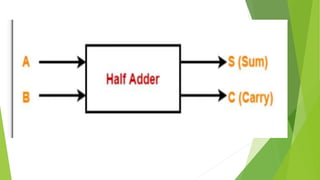
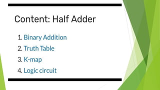
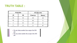
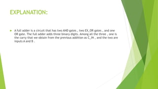
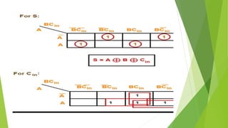
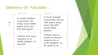
PRESENTATION FOR
DIGITAL AND LOGIC
DESIGN
PRESENTED BY:
HAFEEZA MUSTAFA
TOPPIC :
HALF ADDER
PRESENT
ED BY:
HAFEEZA
MUSTAFA
DEFINITION:
 It is a combinational logic circuit . It is also called two bits adder .
EXPLANATION:
We can design it by connecting one AND gate and one XOR gate . A half adder
circuit consist of two input terminal namely A and B both of these add two input
digits and generate the output . IN form of carry and other output sum .Thus
there are two outputs . The output that obtains from the XOR gate is sum of the
both bits numbers . The output obtained from AND gate is called carry .
Half adder designing:
 We can design half adder by using following steps .
TRUTH TABLE :
2 VARIABLE K-MAP FOR SUM AND
CARRY:
BOLEAN EXPRESSION:
HALF ADDER DIAGRAM:
 BY using XOR expression.
TOPPIC :
FULL ADDER
PRESENT
ED BY:
HAFEEZA
MUSTAFA
Definition:
Full Adder is the adder which adds three inputs and produces two outputs. The
first two inputs are A and B and the third input is an input carry as C-IN. The
output carry is designated as C-OUT and the normal output is designated as S
which is SUM.
EXPLANATION:
 A full adder is a circuit that has two AND gates , two EX_OR gates , and one
OR gate. The full adder adds three binary digits. Among all the three , one is
the carry that we obtain from the previous addition as C_IN , and the two are
inputs A and B .
Full Adder Block:
K-Map For Sum:
K-Map For Carry:
Bolean Expression Equation Full Adder :
Deference Of Full Adder :
Application Of Half And Full Adder :
PRESENTATION FOR DIGITAL AND LOGIC DESIGN.pptx

PRESENTATION FOR DIGITAL AND LOGIC DESIGN.pptx