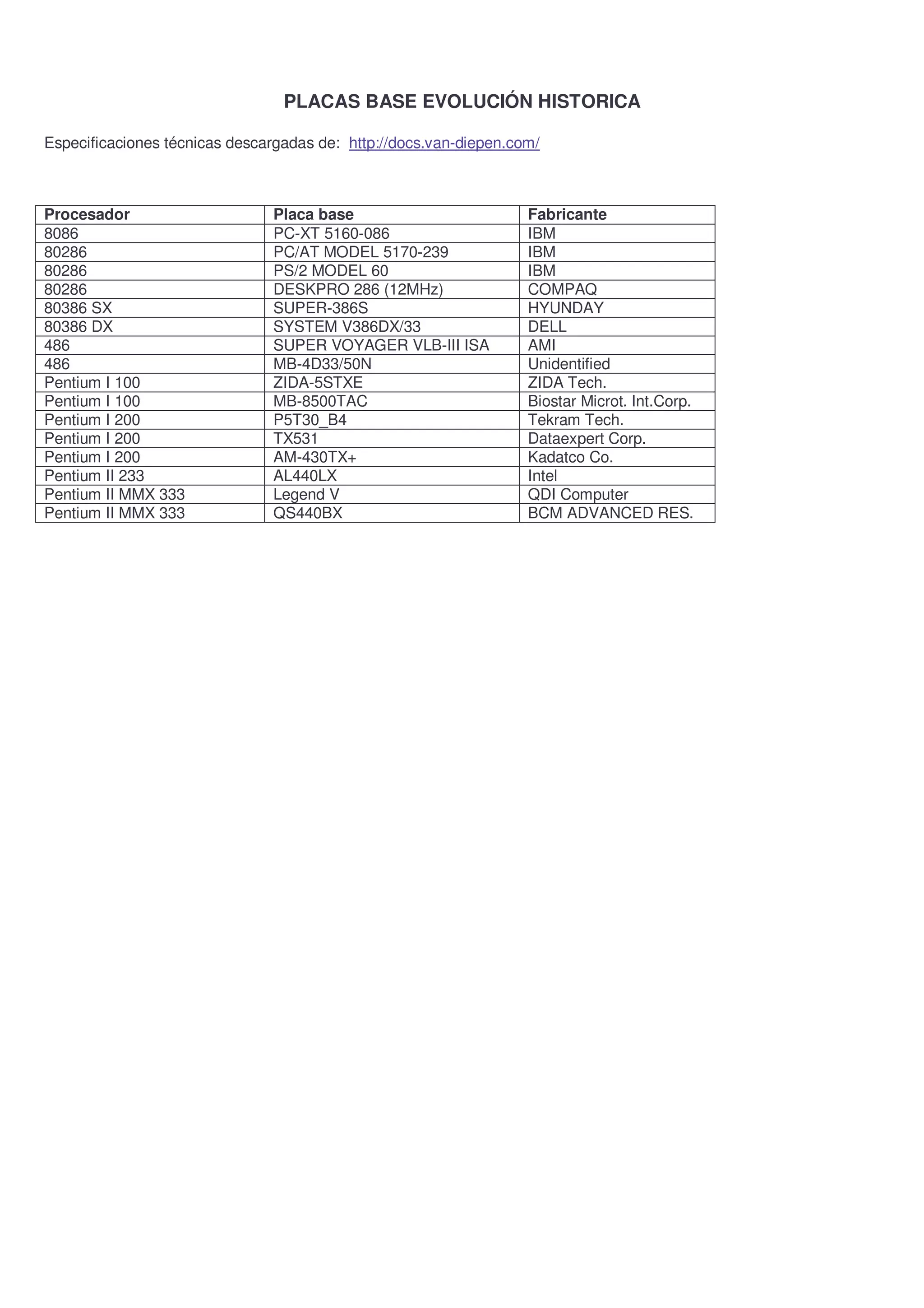
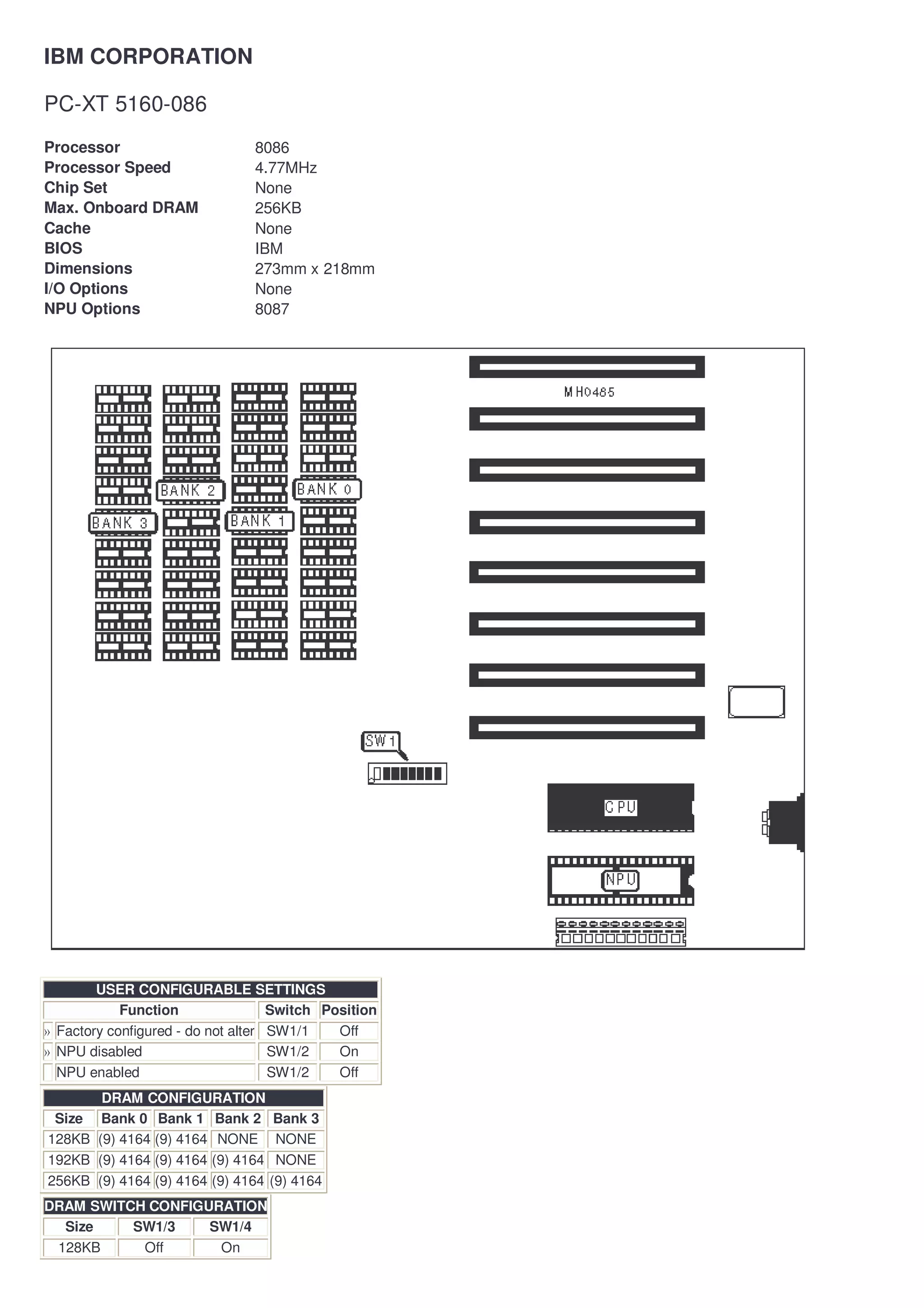
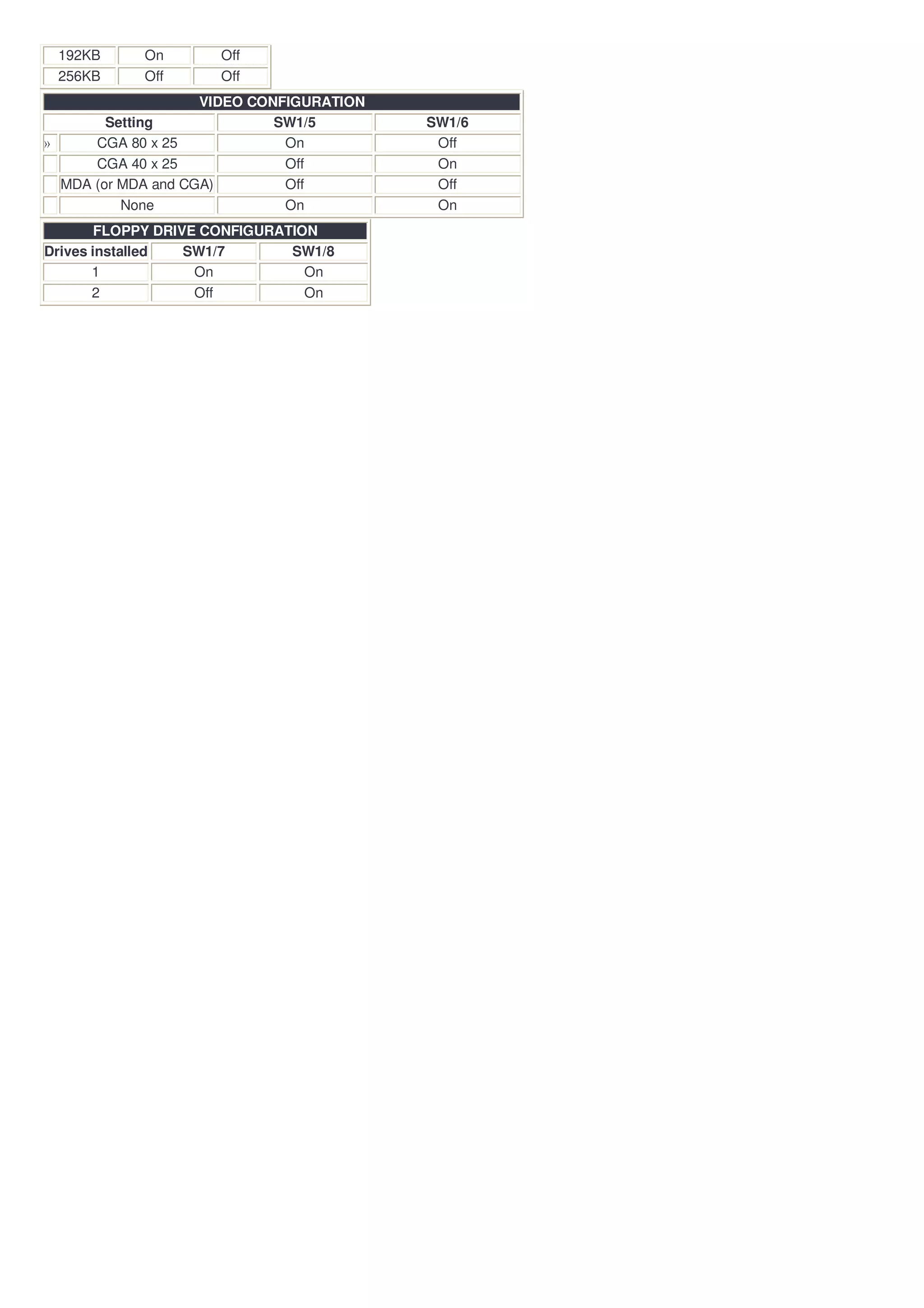
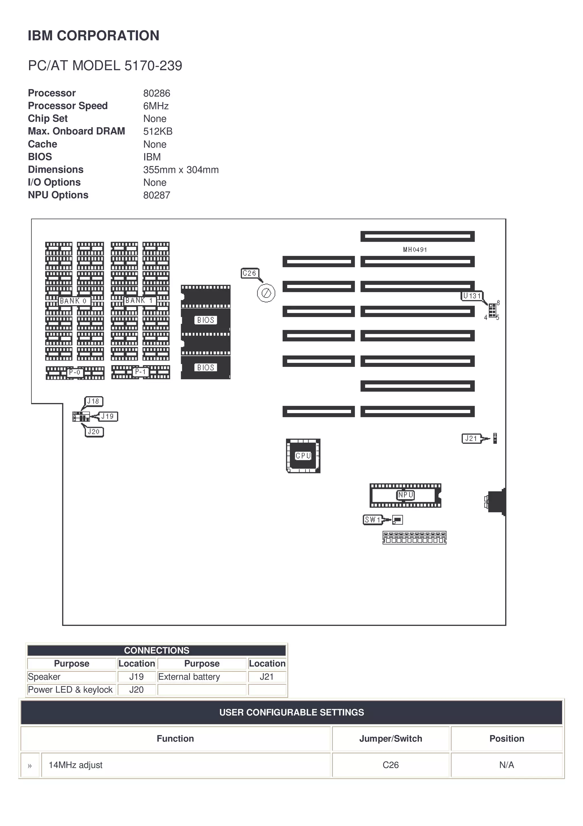
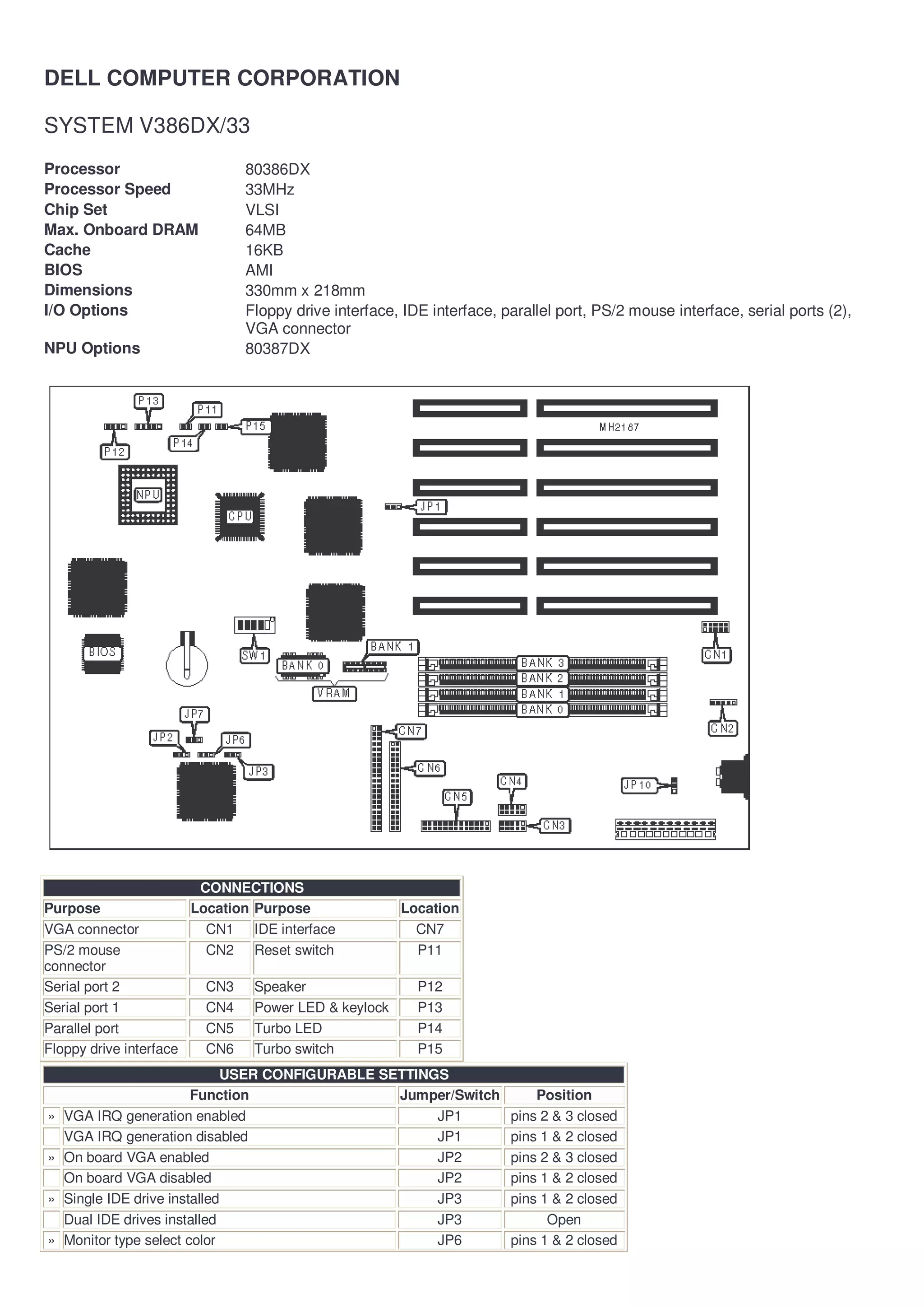
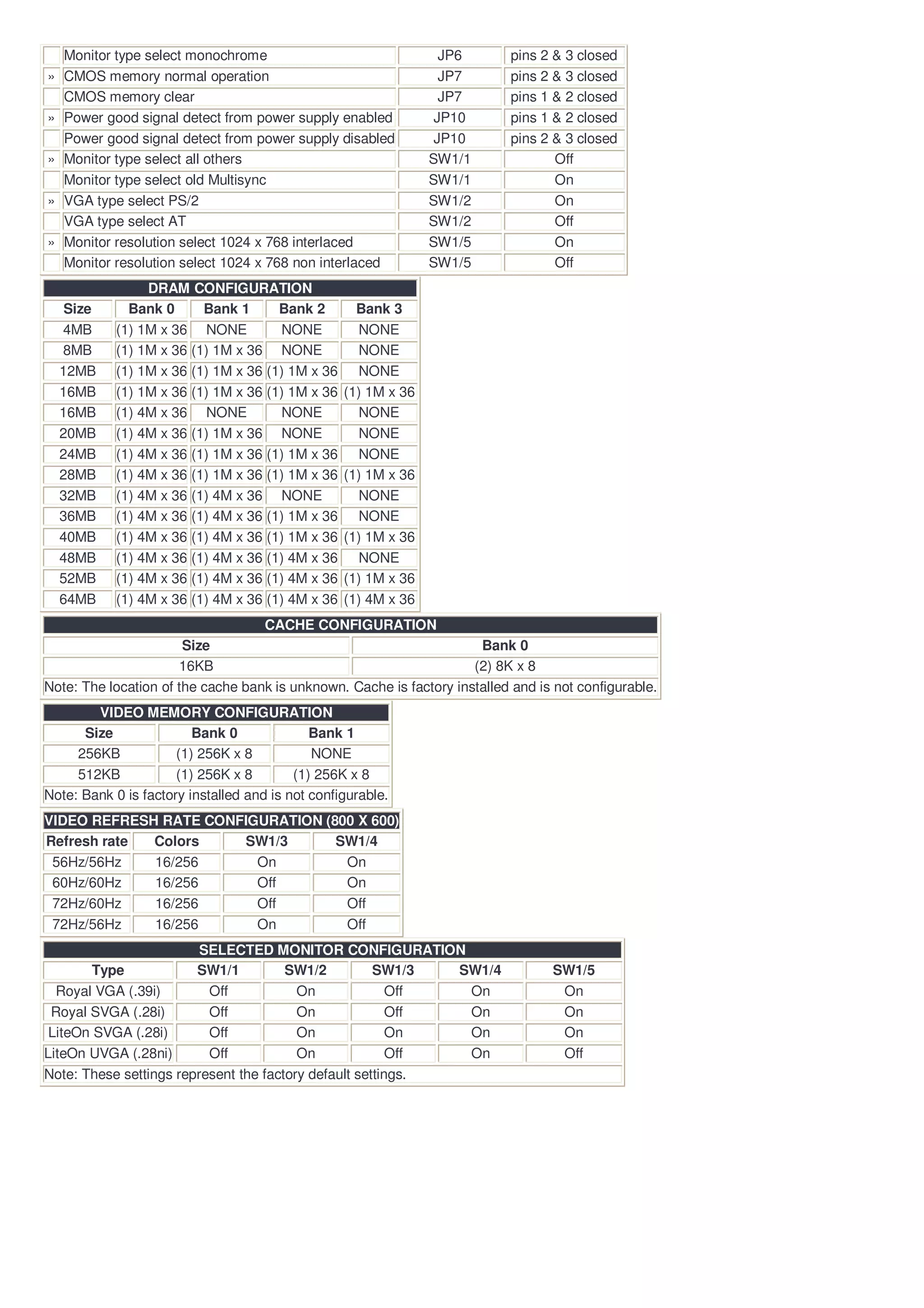
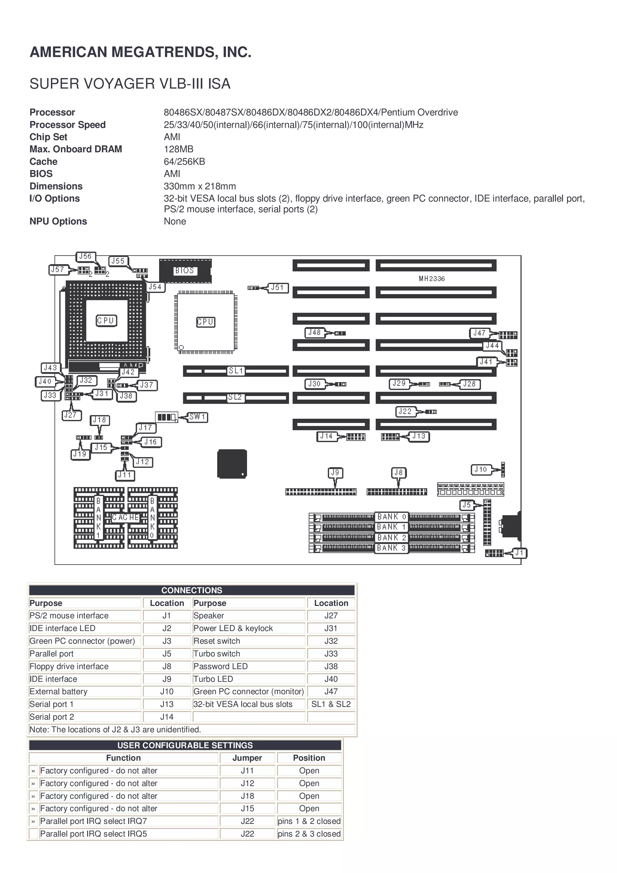
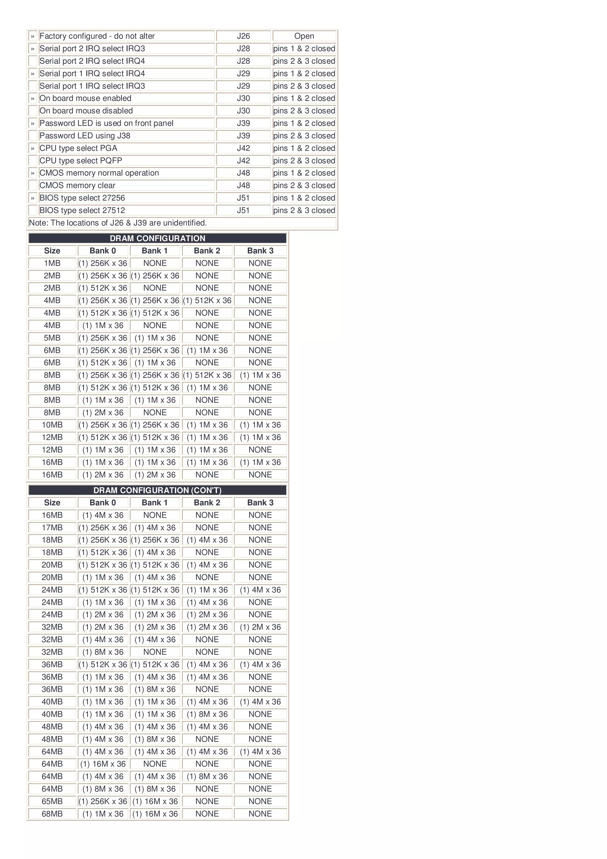
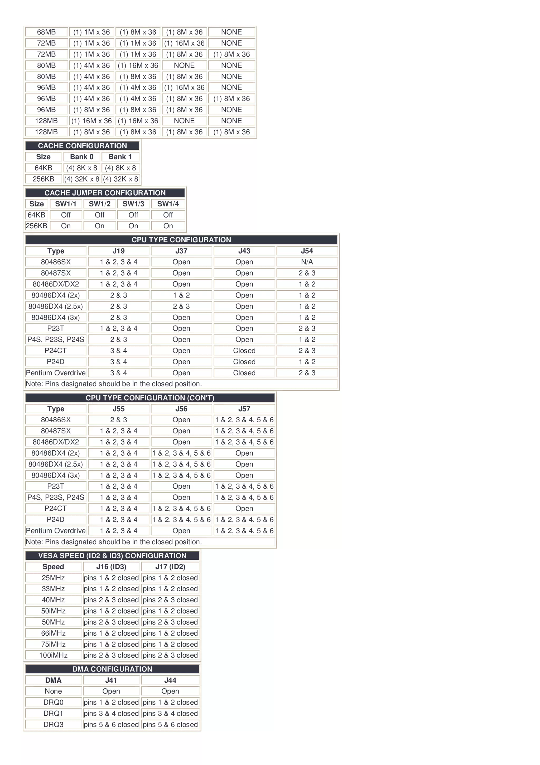
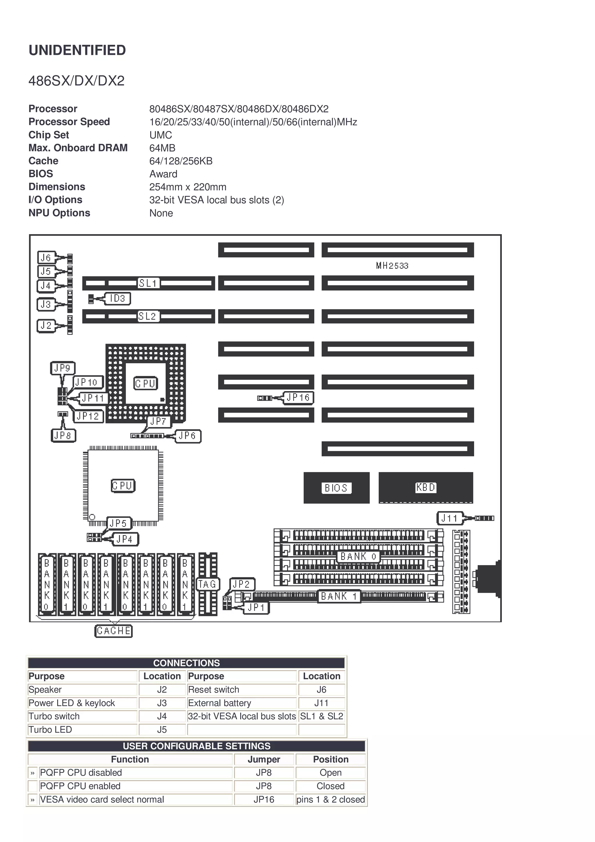
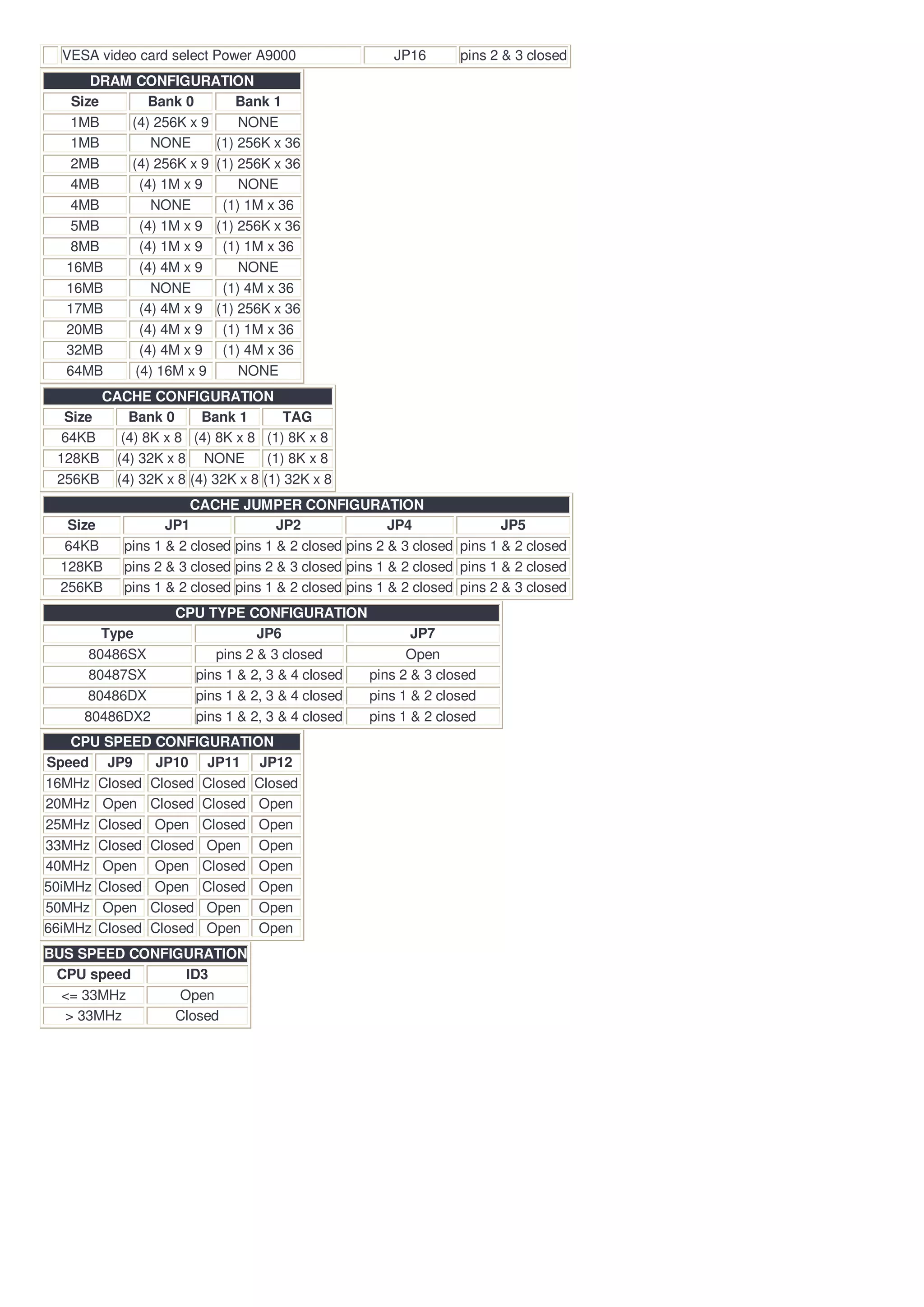
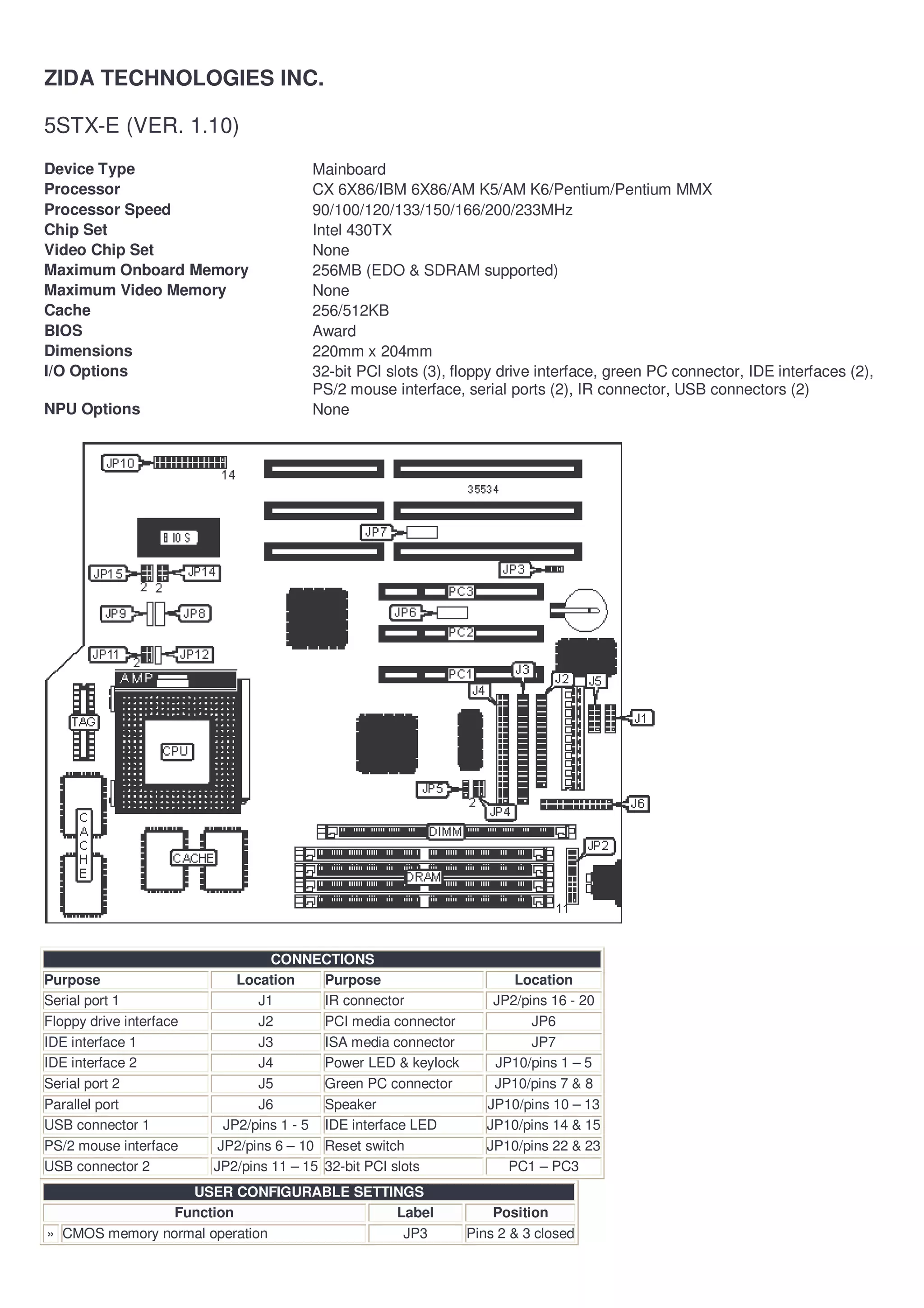
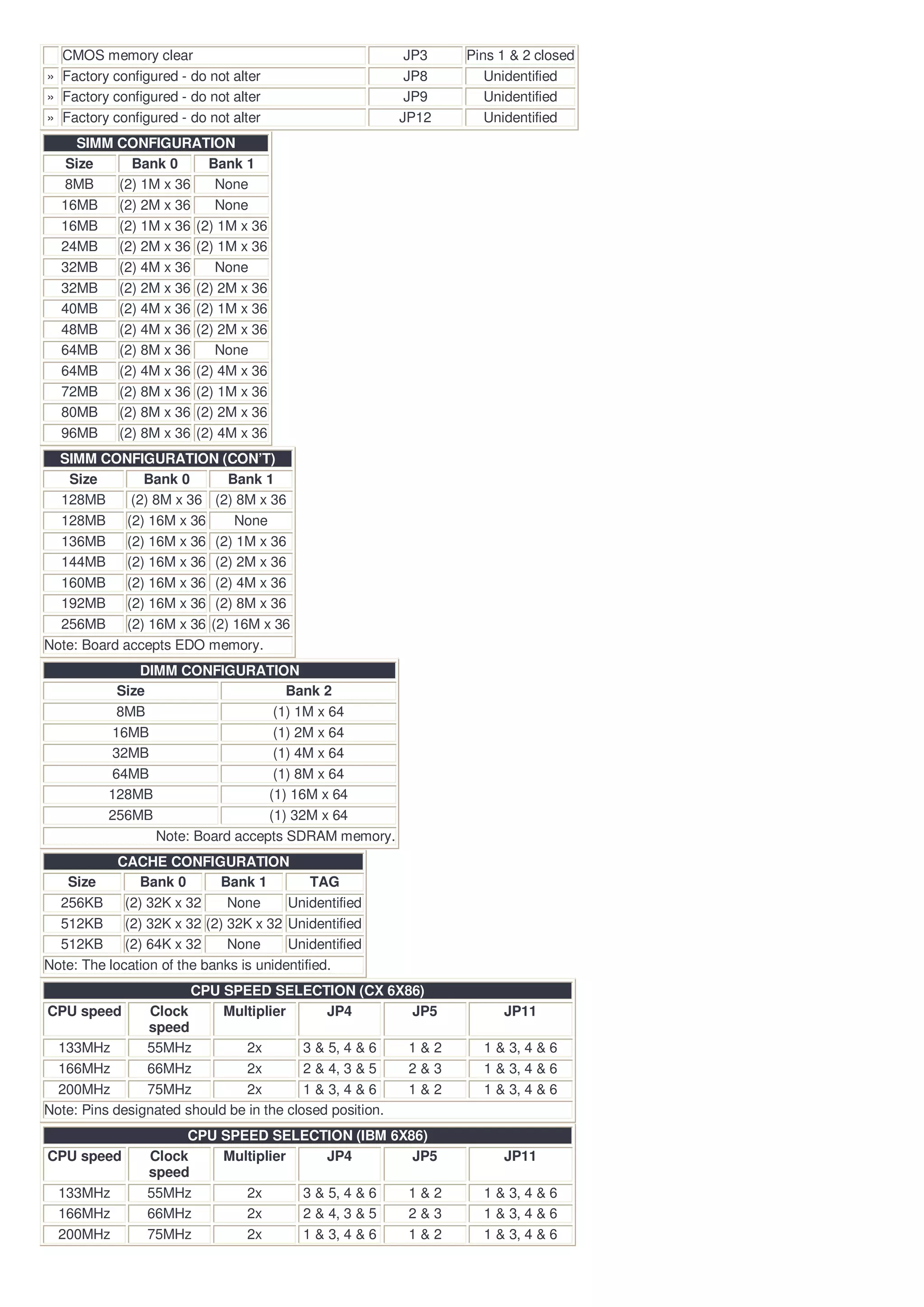
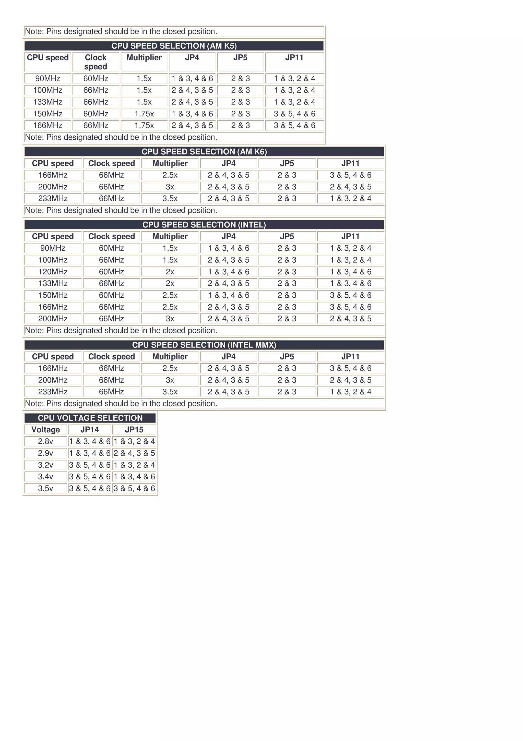
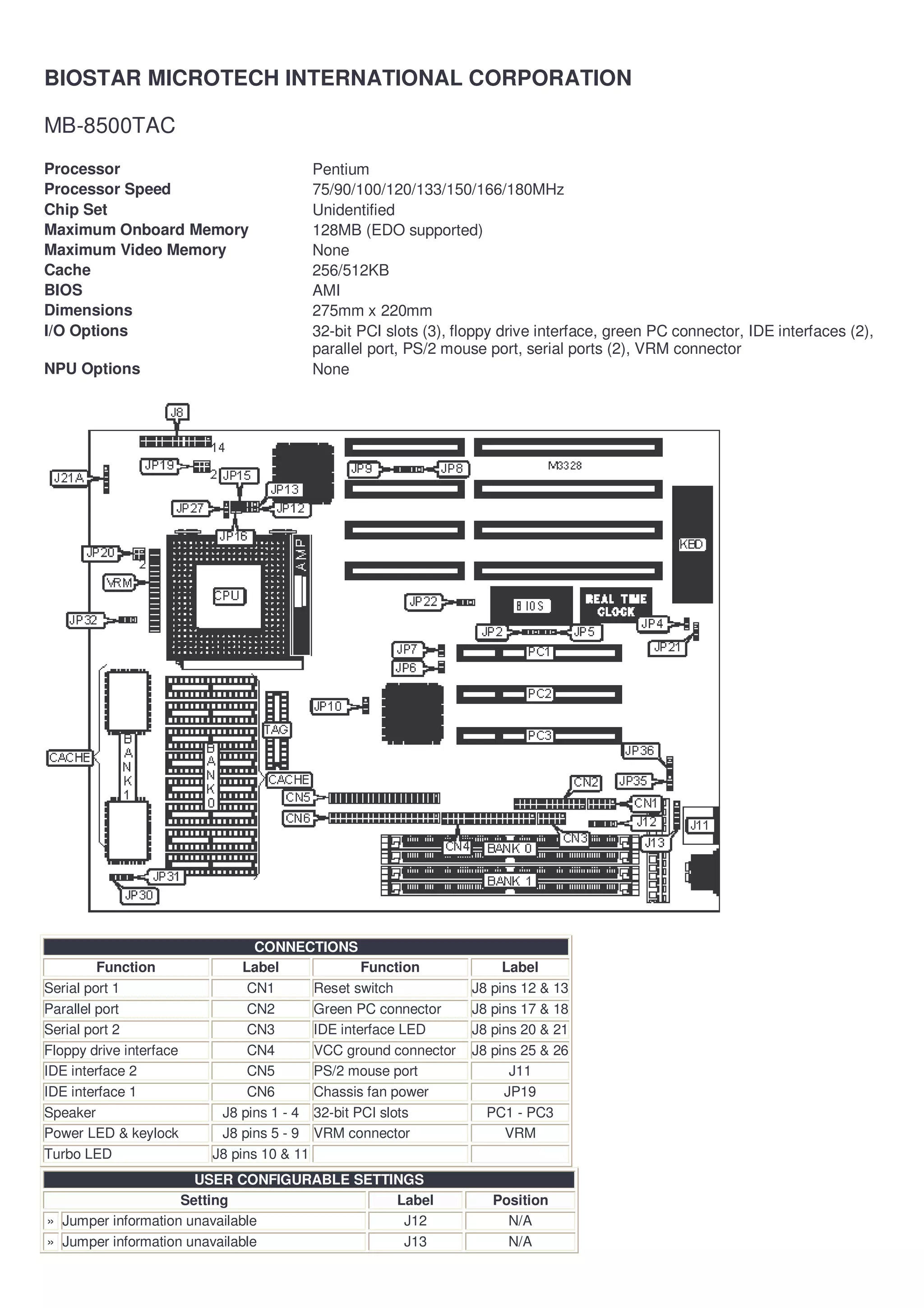
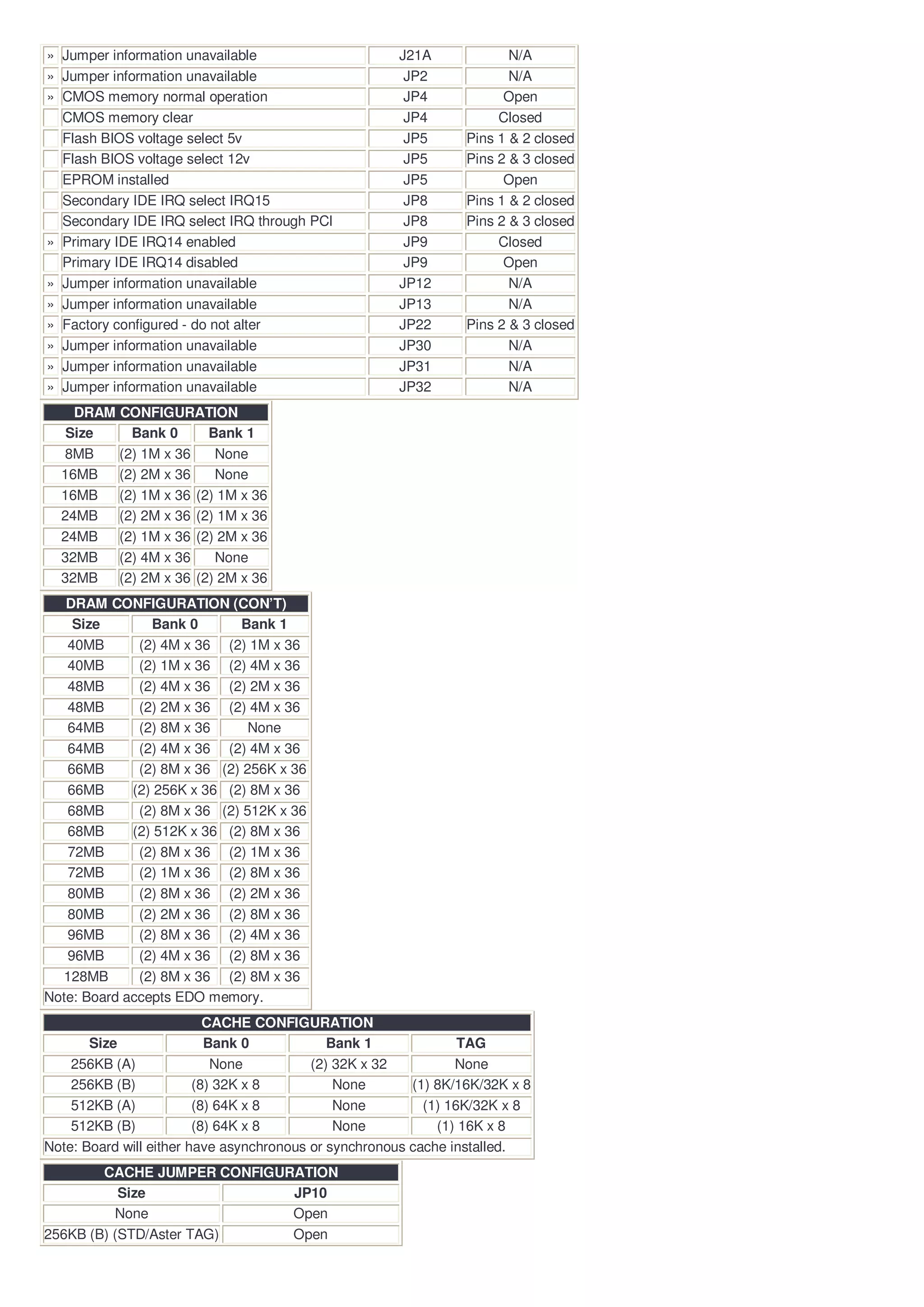
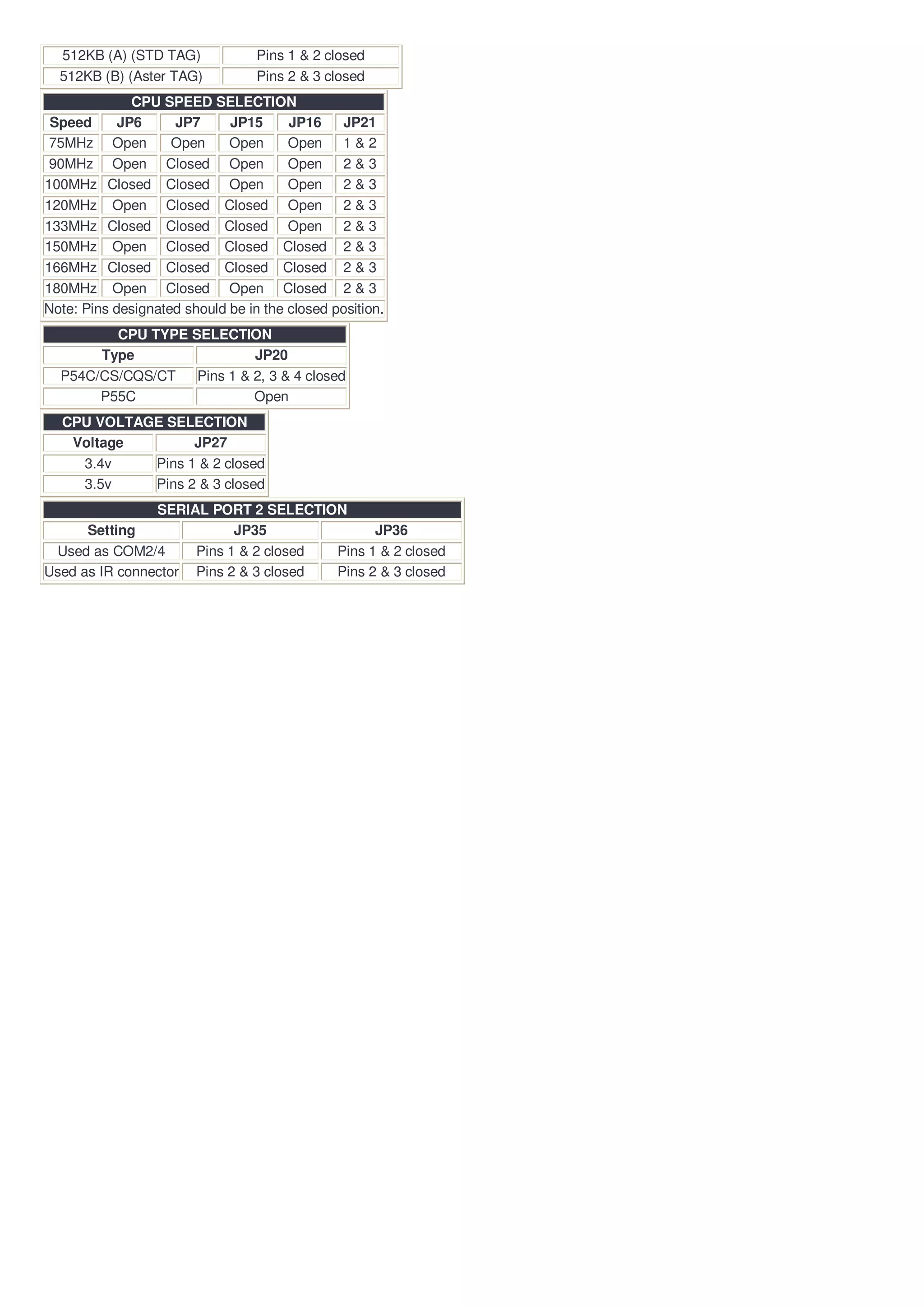
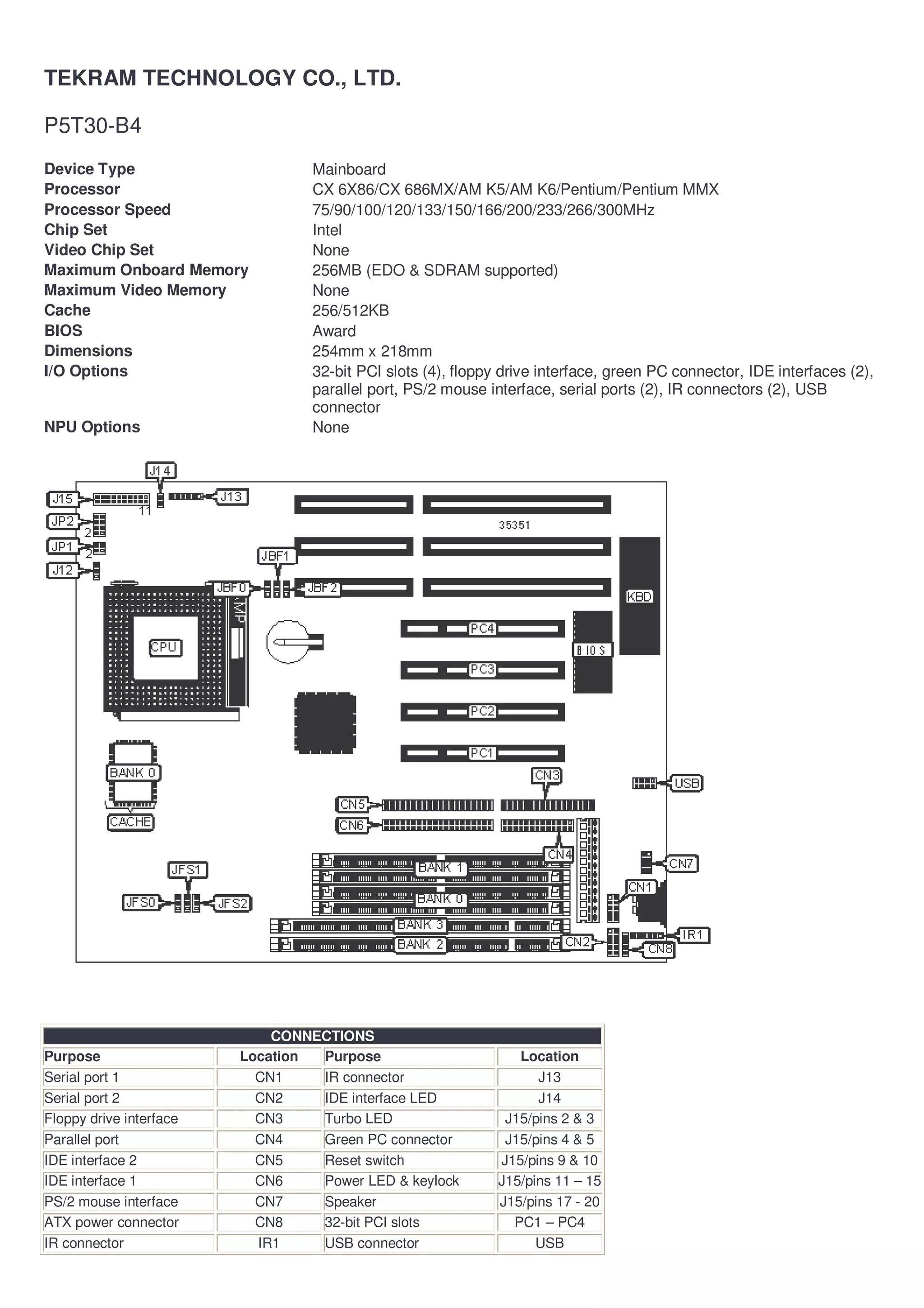
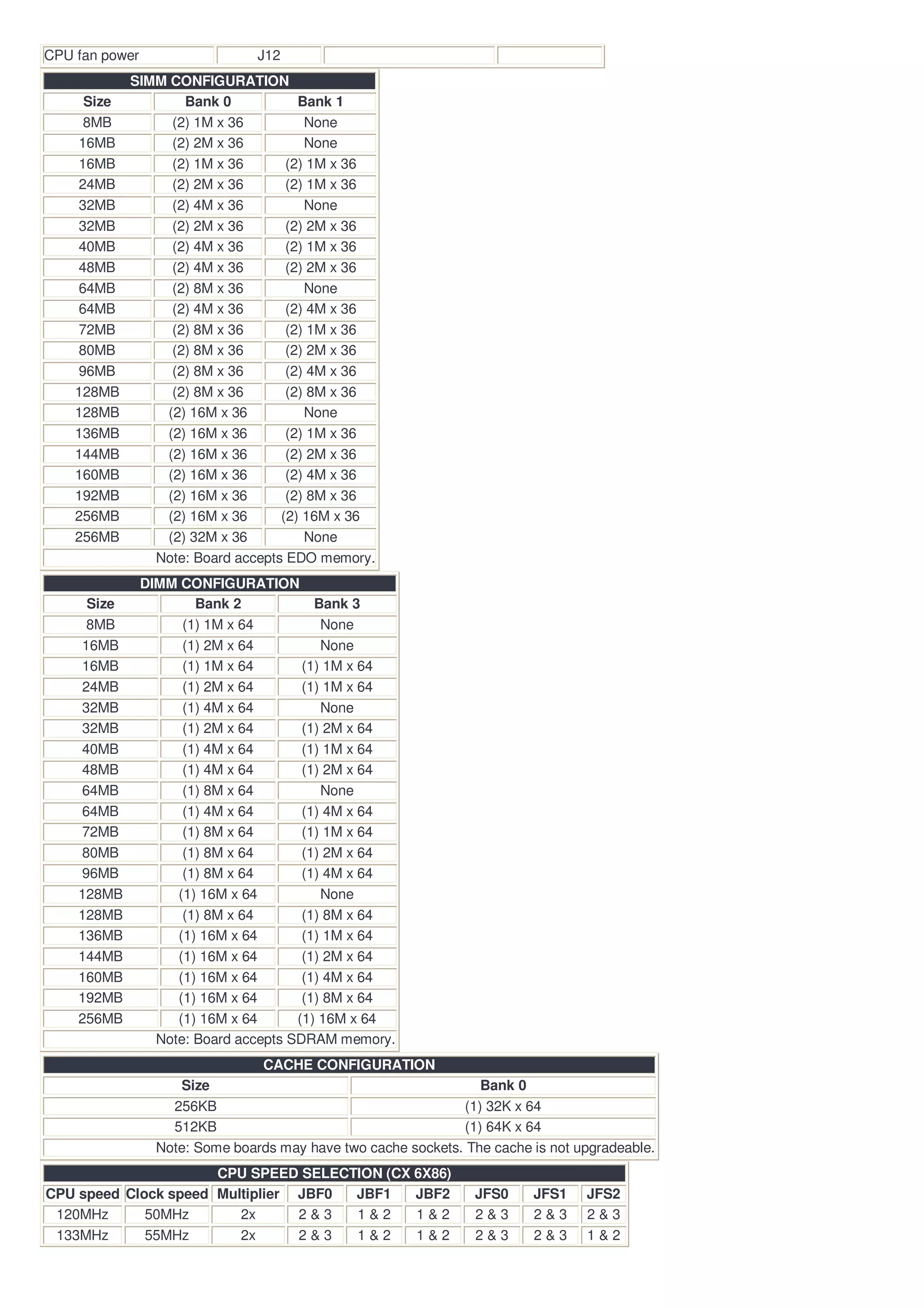
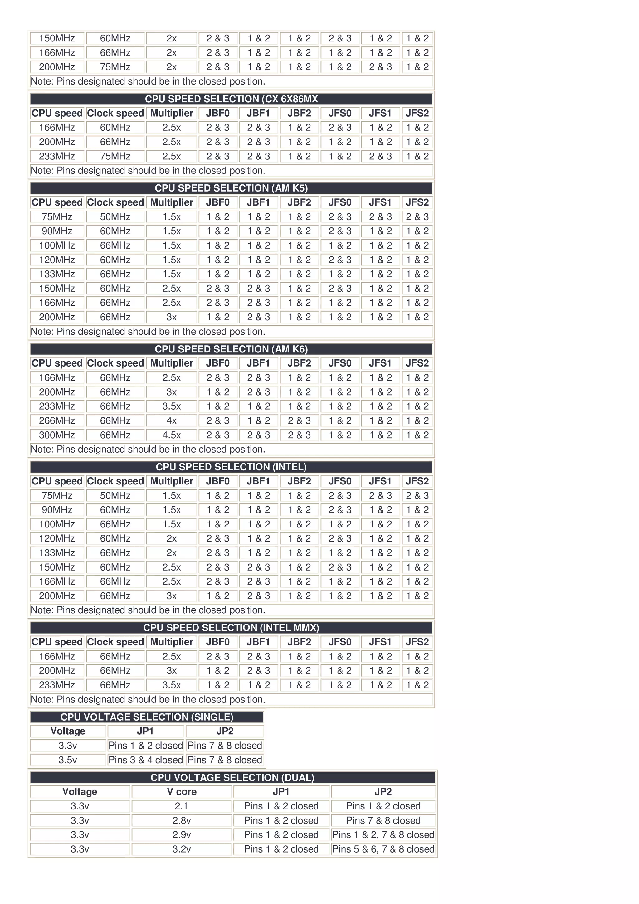
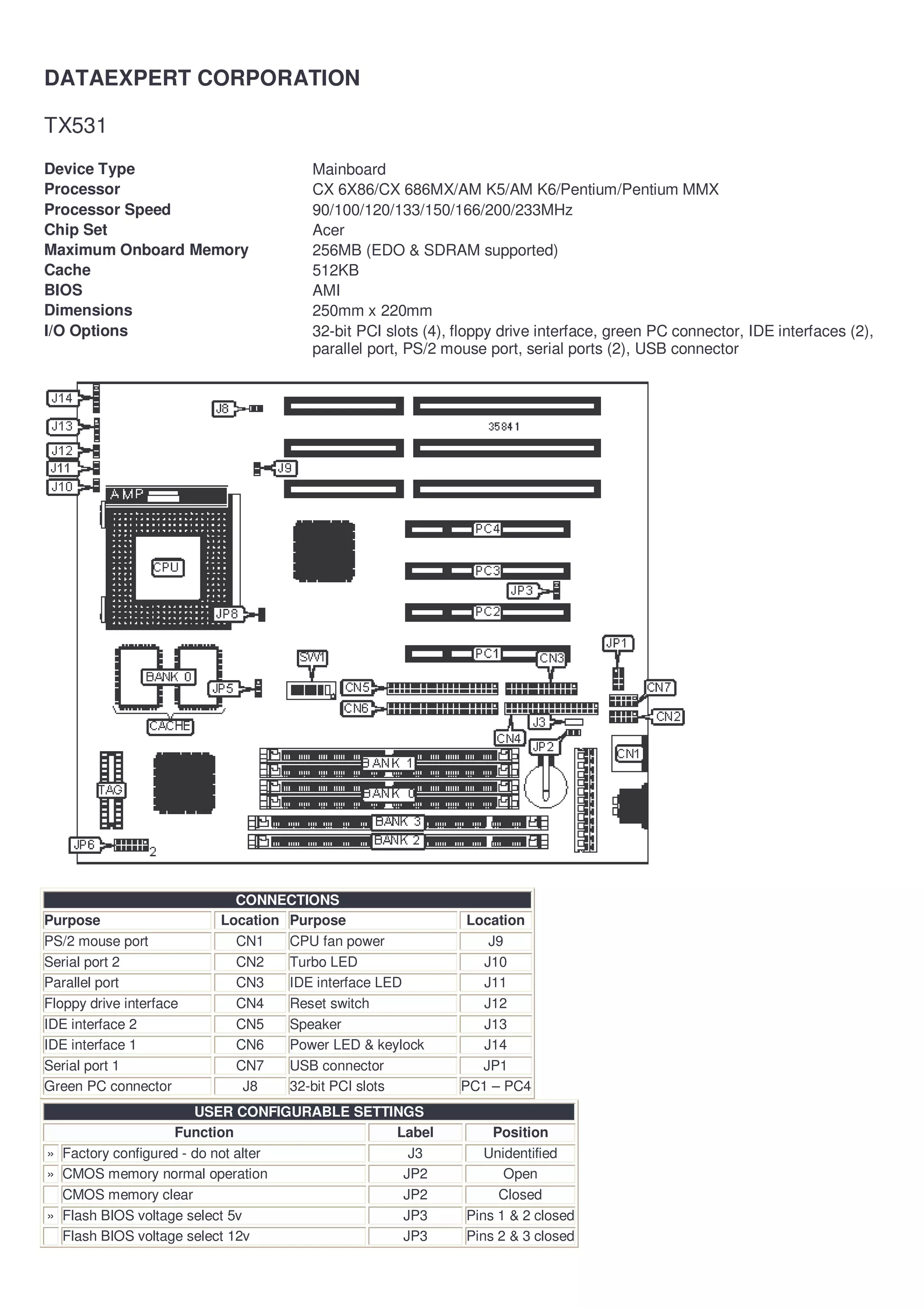
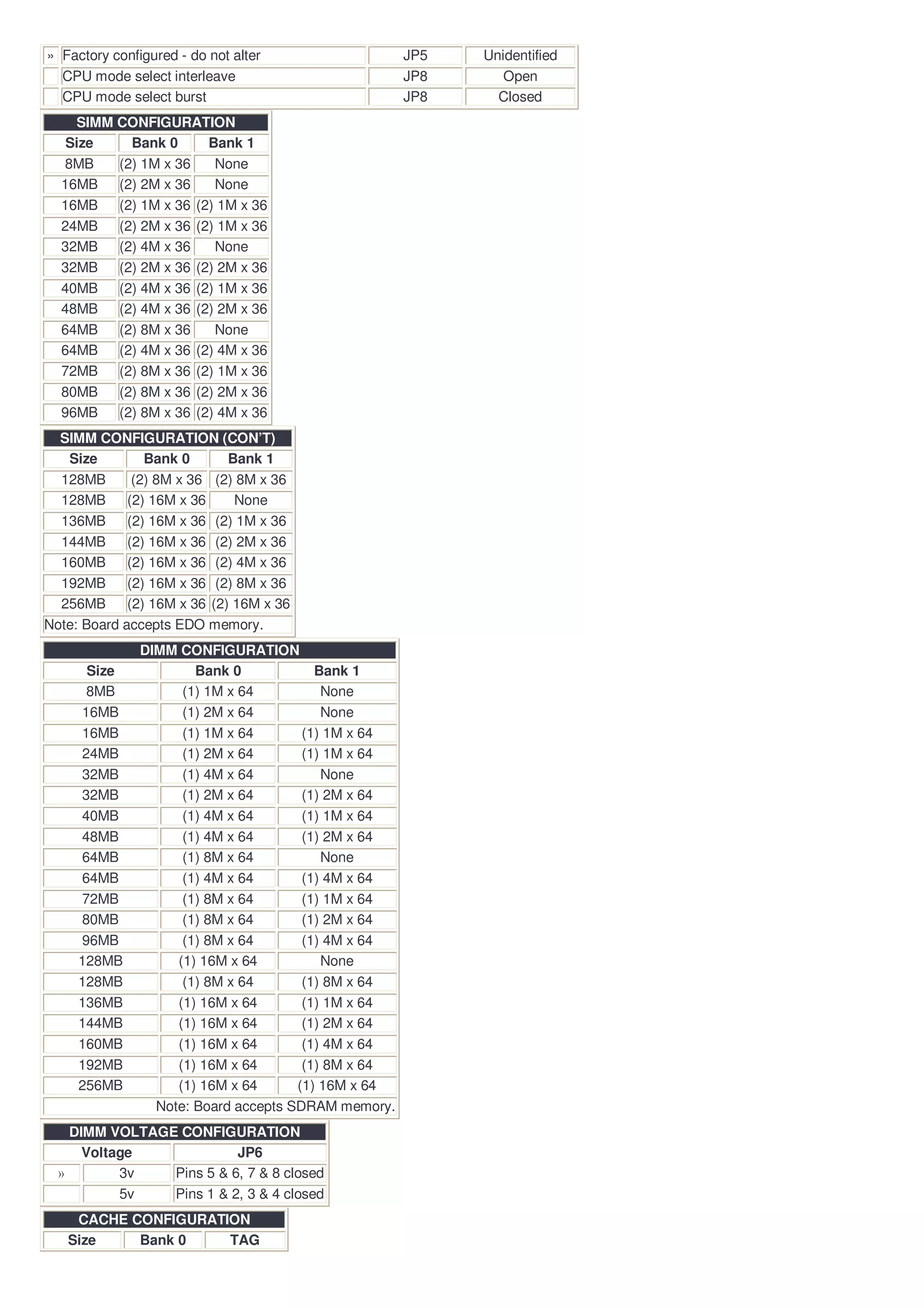
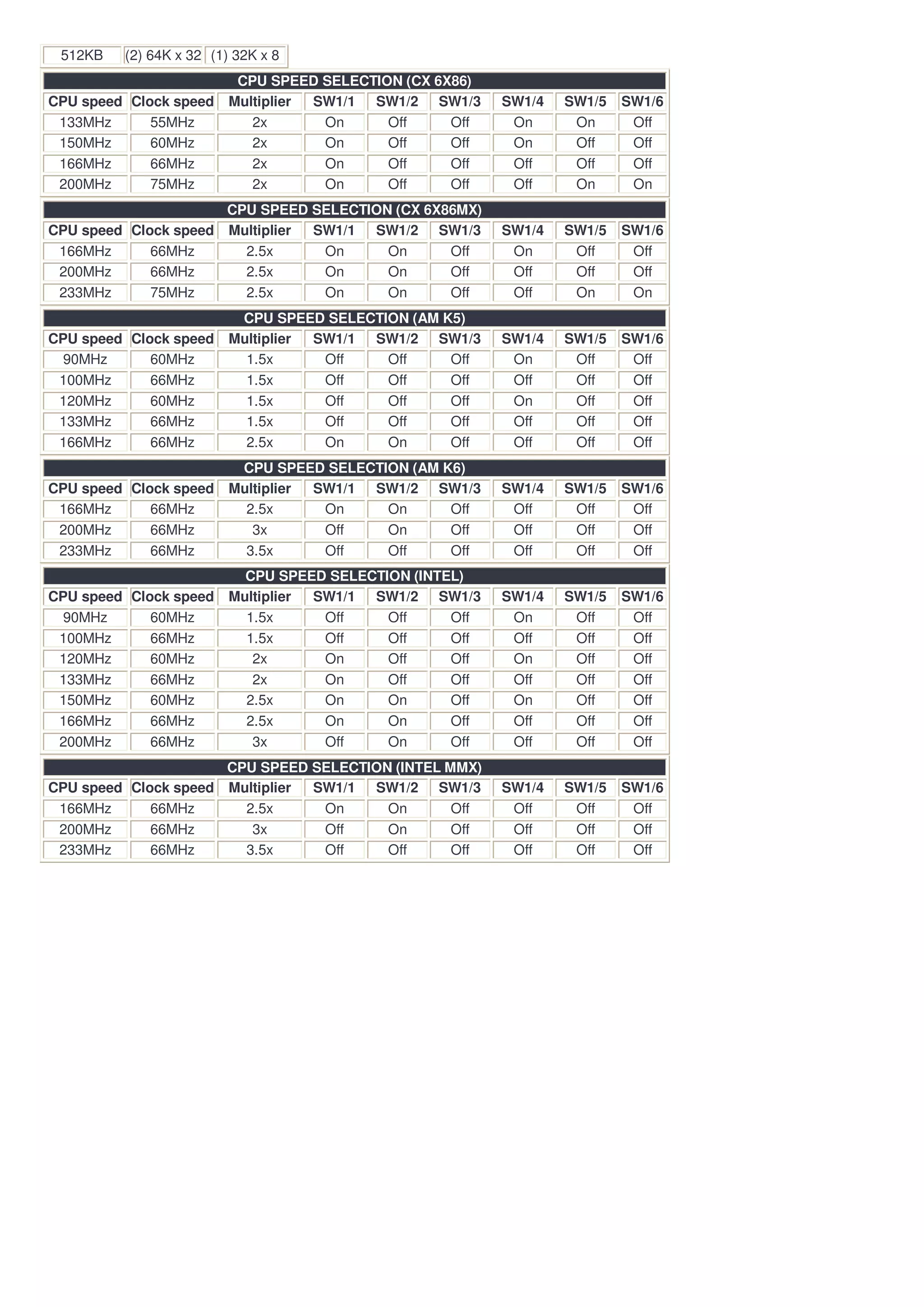
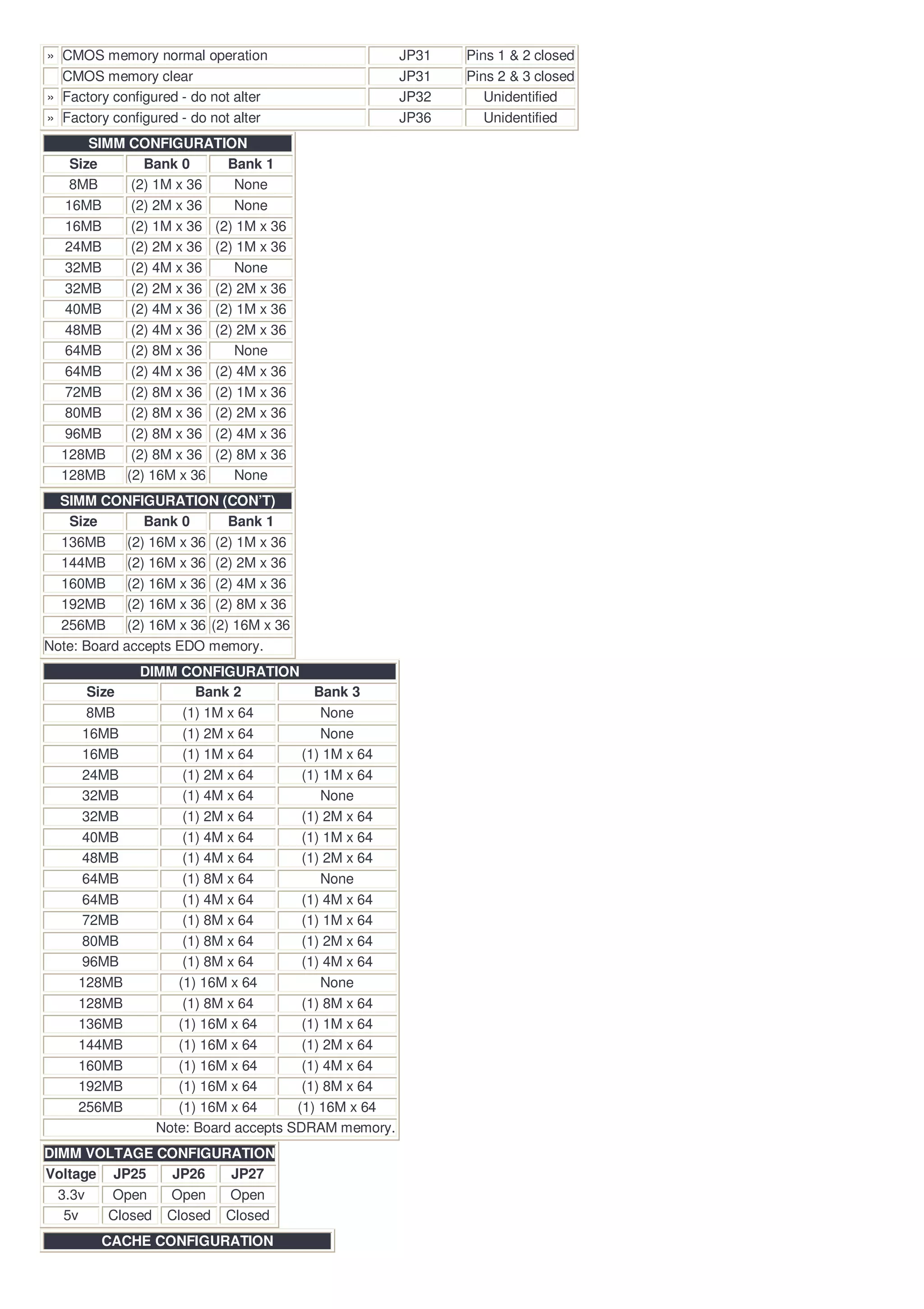
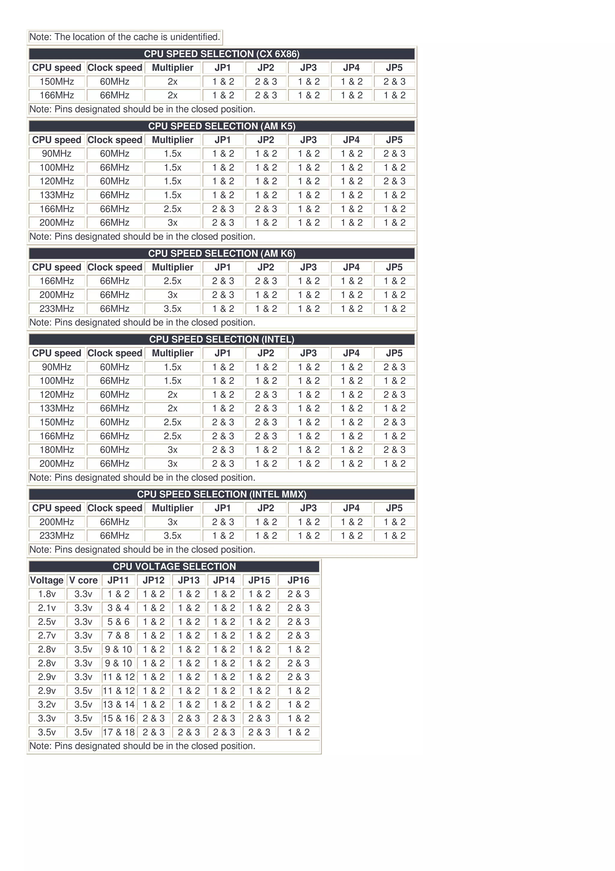
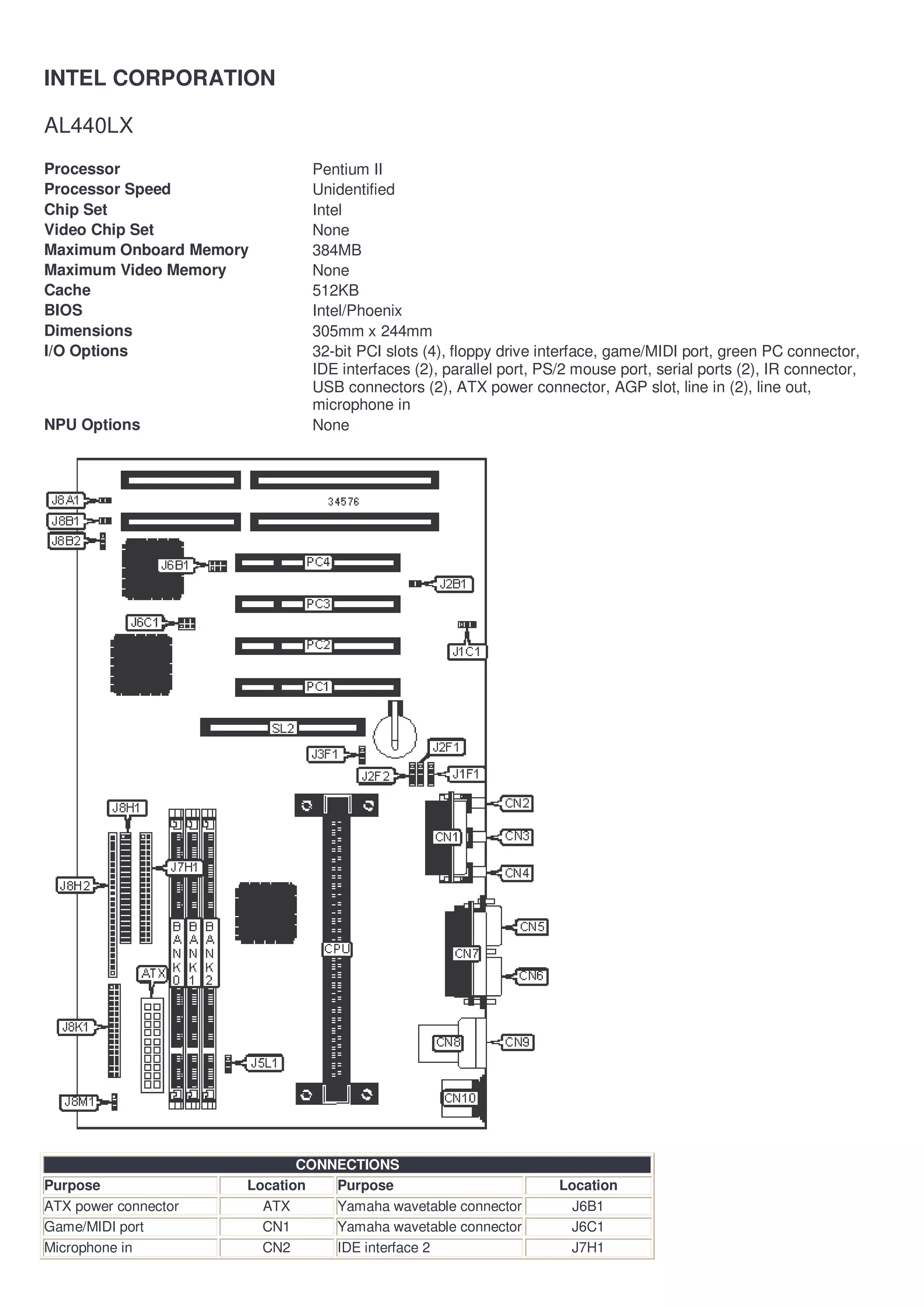
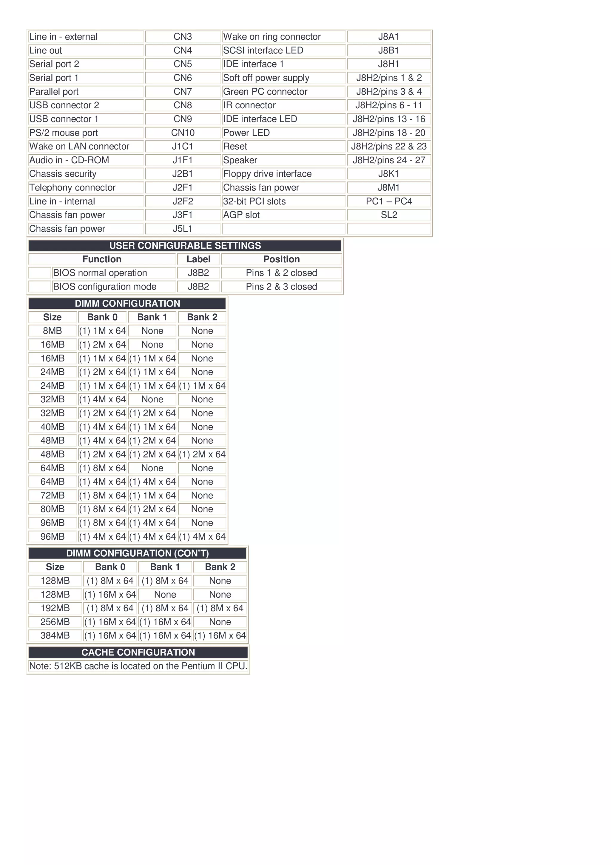
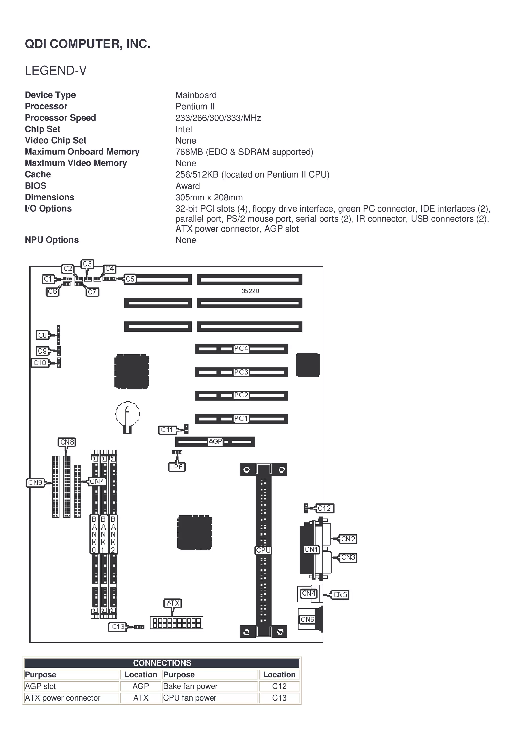
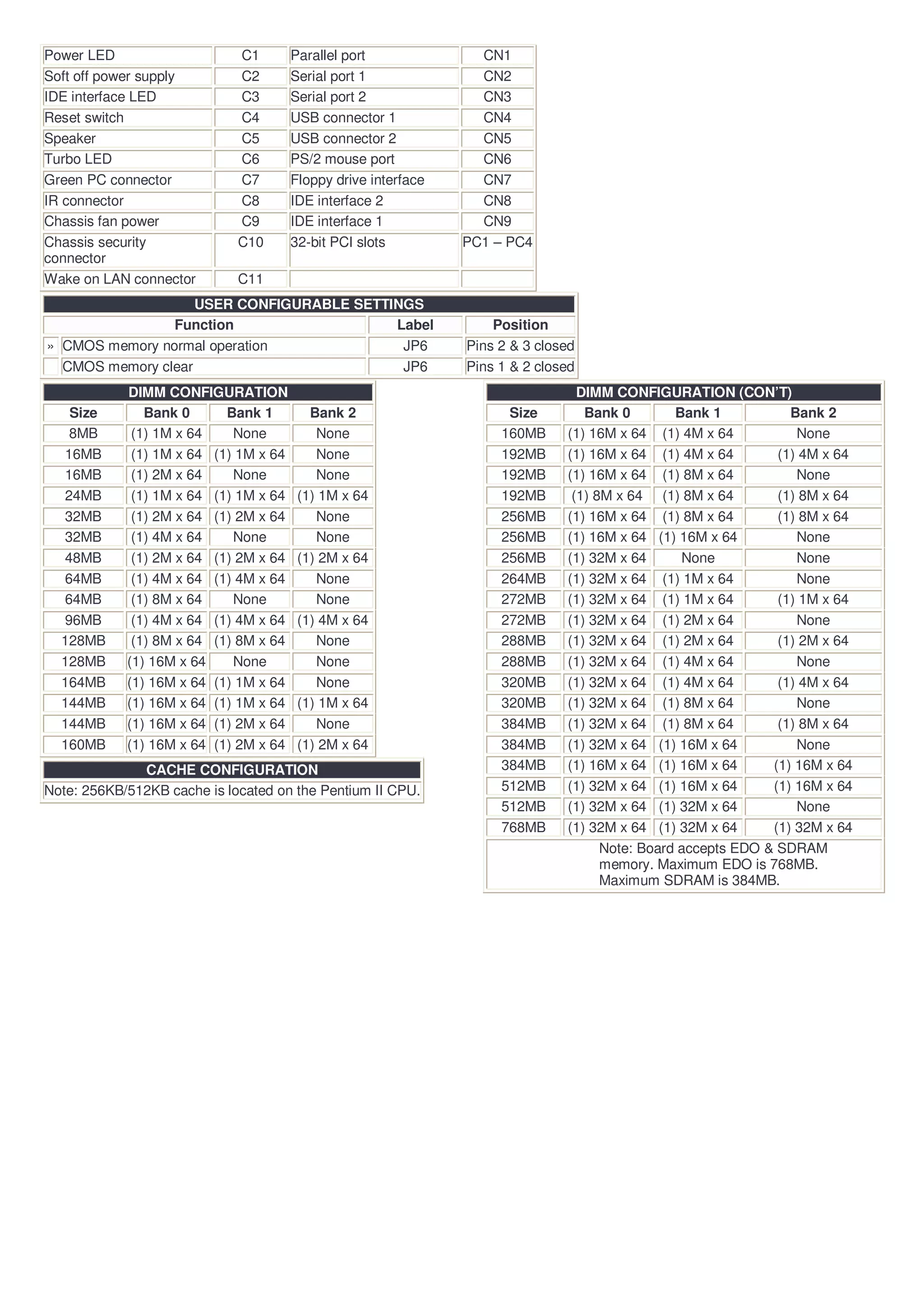
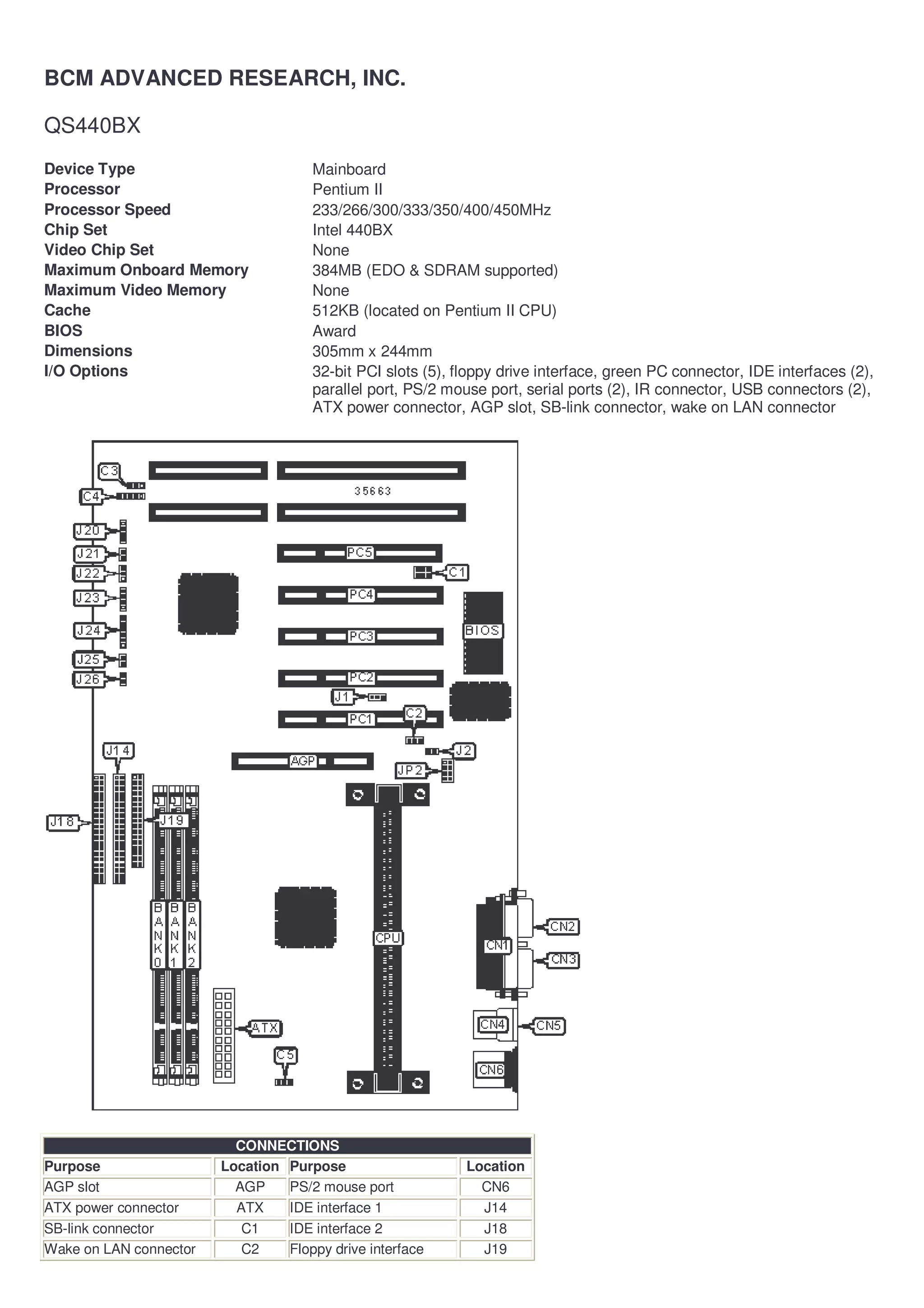
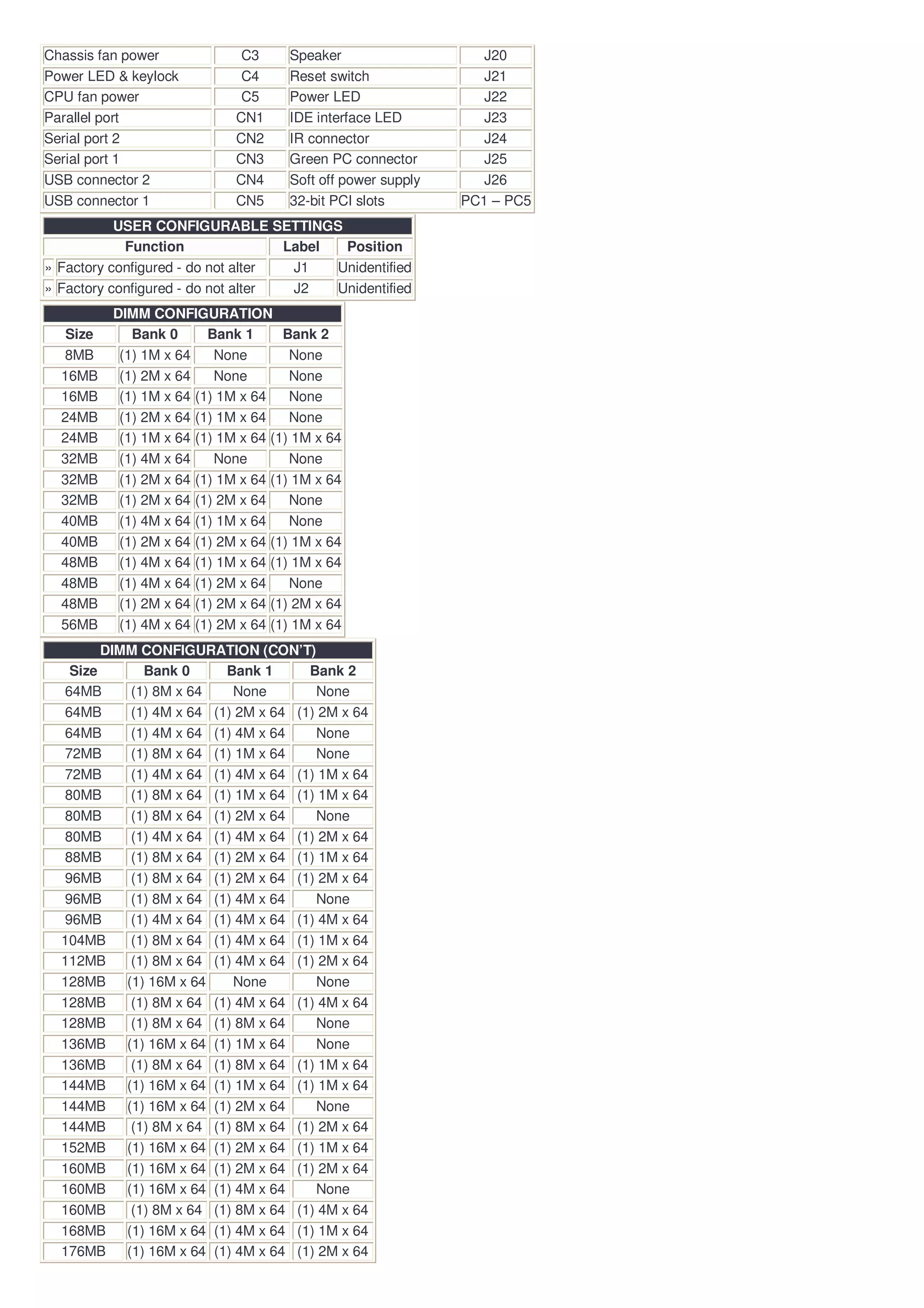
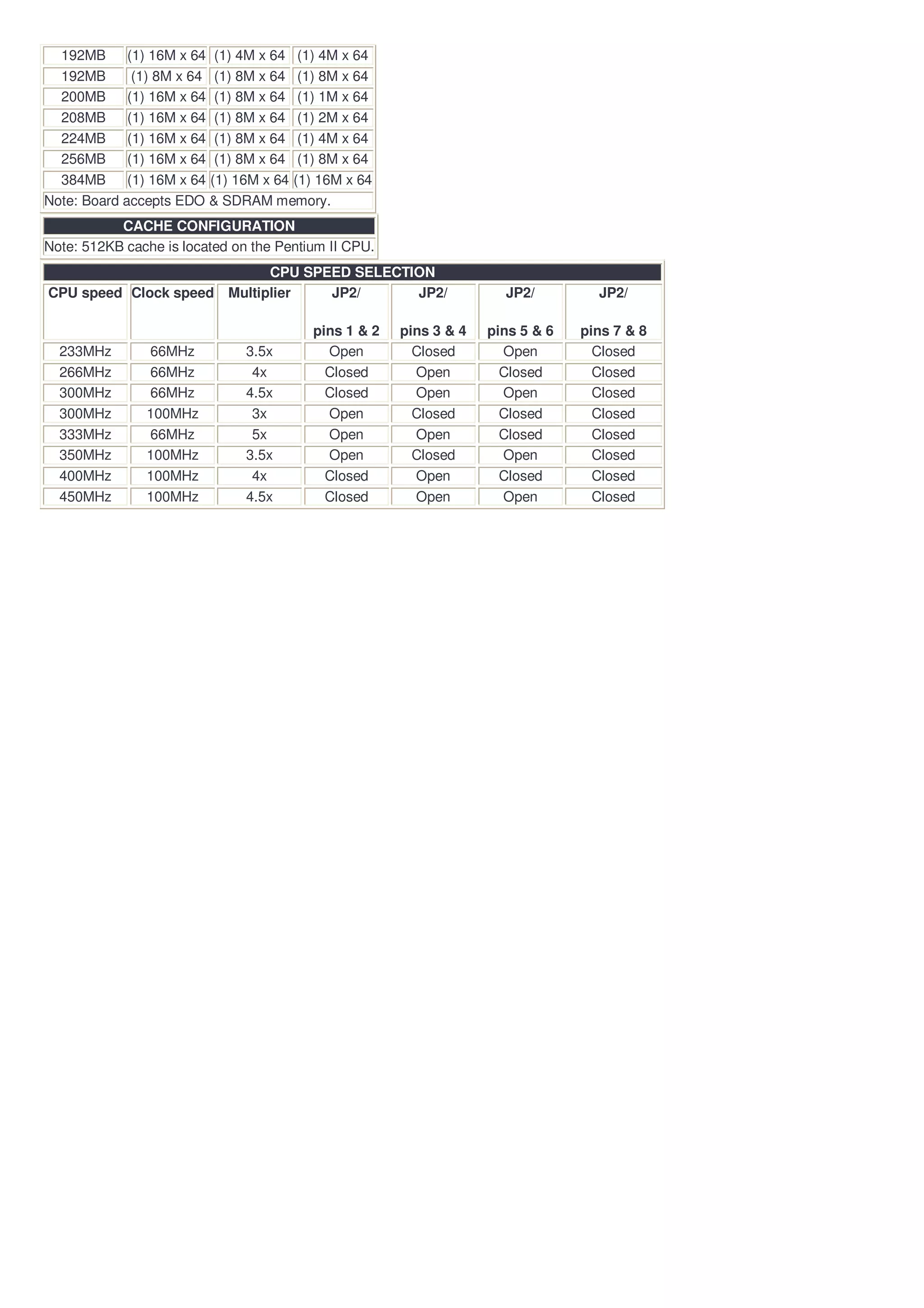
PLACAS BASE EVOLUCIÓN HISTORICA

Especificaciones técnicas descargadas de: http://docs.van-diepen.com/


Procesador                     Placa base                          Fabricante
8086                           PC-XT 5160-086                      IBM
80286                          PC/AT MODEL 5170-239                IBM
80286                          PS/2 MODEL 60                       IBM
80286                          DESKPRO 286 (12MHz)                 COMPAQ
80386 SX                       SUPER-386S                          HYUNDAY
80386 DX                       SYSTEM V386DX/33                    DELL
486                            SUPER VOYAGER VLB-III ISA           AMI
486                            MB-4D33/50N                         Unidentified
Pentium I 100                  ZIDA-5STXE                          ZIDA Tech.
Pentium I 100                  MB-8500TAC                          Biostar Microt. Int.Corp.
Pentium I 200                  P5T30_B4                            Tekram Tech.
Pentium I 200                  TX531                               Dataexpert Corp.
Pentium I 200                  AM-430TX+                           Kadatco Co.
Pentium II 233                 AL440LX                             Intel
Pentium II MMX 333             Legend V                            QDI Computer
Pentium II MMX 333             QS440BX                             BCM ADVANCED RES.
IBM CORPORATION

PC-XT 5160-086
Processor                           8086
Processor Speed                     4.77MHz
Chip Set                            None
Max. Onboard DRAM                   256KB
Cache                               None
BIOS                                IBM
Dimensions                          273mm x 218mm
I/O Options                         None
NPU Options                         8087


           USER CONFIGURABLE SETTINGS
               Function                Switch Position


     Factory configured - do not alter SW1/1    Off


     NPU disabled                      SW1/2    On
     NPU enabled                       SW1/2    Off
             DRAM CONFIGURATION
     Size    Bank 0 Bank 1 Bank 2 Bank 3
    128KB   (9) 4164 (9) 4164 NONE NONE
    192KB   (9) 4164 (9) 4164 (9) 4164 NONE
    256KB   (9) 4164 (9) 4164 (9) 4164 (9) 4164
DRAM SWITCH CONFIGURATION
  Size    SW1/3    SW1/4
 128KB     Off      On
192KB     On       Off
    256KB     Off      Off
                      VIDEO CONFIGURATION
          Setting              SW1/5        SW1/6


        CGA 80 x 25             On           Off
        CGA 40 x 25             Off          On
    MDA (or MDA and CGA)        Off          Off
            None                On           On
        FLOPPY DRIVE CONFIGURATION
Drives installed   SW1/7       SW1/8
       1            On           On
       2            Off          On
IBM CORPORATION

PC/AT MODEL 5170-239
Processor                  80286
Processor Speed            6MHz
Chip Set                   None
Max. Onboard DRAM          512KB
Cache                      None
BIOS                       IBM
Dimensions                 355mm x 304mm
I/O Options                None
NPU Options                80287


                     CONNECTIONS
     Purpose        Location       Purpose       Location
Speaker               J19    External battery      J21
Power LED & keylock   J20

                                            USER CONFIGURABLE SETTINGS

                              Function                               Jumper/Switch   Position


    14MHz adjust                                                         C26           N/A


     Monitor type select color                                                            SW1   On


     Monitor type select monochrome                                                       SW1   Off

Note:Variable resistor C26 should not be altered except by competently trained technicians.

                         DRAM CONFIGURATION
     Size           Bank 0         P-0         Bank 1         P-0
    256KB       (16) ZA1250NL (2) ZA1250NL      NONE         NONE
    512KB       (16) ZA1250NL (2) ZA1250NL (16) ZA1250NL (2) ZA1250NL
DRAM JUMPER CONFIGURATION
    Size            J18
   256KB     pins 1 & 2 closed
   512KB     pins 2 & 3 closed
           BIOS CONFIGURATION
         Size                 U131
         2716        pins 1 & 8, 2 & 7 closed
         2732        pins 3 & 6, 4 & 5 closed
IBM CORPORATION

PS/2 MODEL 60
Processor           80286
Processor Speed     10MHz
Chip Set            None
Max. Onboard DRAM   4MB
Cache               None
BIOS                IBM
Dimensions          330.2mm x 218.4mm
I/O Options         Serial port, parallel port, pointing device connector, video port

                    floppy drive interface, hard drive interface slot, video expansion slot
NPU Options         80287
CONNECTIONS
Purpose                 Location Purpose                  Location
Power supply               J2    Video port                 J10
Floppy drive               J3    Serial port                J11
Battery/speaker            J5    Parallel port              J12
Video expansion slot       J8    Pointing device            J13
Hard drive interface       J9    Keyboard                   J14
slot
                            DRAM CONFIGURATION
          Size                       Bank 0                            Bank 1
          1MB                     (2) 256K x 9                      (2) 256K x 9
          2MB                       (2) 1M x 9                         NONE
         2.5MB                    (2) 256K x 9                       (2) 1M x 9
          4MB                       (2) 1M x 9                       (2) 1M x 9
Note:Onboard memory does not have to be full in order to utilize memory expansion cards.

Memory configurations are unverified.
COMPAQ COMPUTER CORPORATION

DESKPRO 286 (12MHz)
Processor                   80286
Processor Speed             12MHz
Chip Set                    ETEQ
Max. Onboard DRAM           2.125MB
Cache                       None
BIOS                        Compaq
Dimensions                  330mm x 218mm
I/O Options                 None
NPU Options                 80287


                                   CONNECTIONS
Purpose                         Location Purpose                              Location
Fixed drive power                 J109   Proprietary keyboard connector         J116
Fixed drive/Tape backup power     J110   Main power                             J117
Floppy drive power                J111   External battery                       J118
Floppy drive power                J112   Keylock                                J119
Monitor power                     J113   Onboard power LED                     LED1
Speaker                           J115
                                              USER CONFIGURABLE SETTINGS
                           Function                                   Jumper/Switch                         Position


    Oscillator type select single package                                   E3                               Closed
    Oscillator type select dual package                                     E3                                Open


    Memory operation generation select discrete gate                        E4                          pins 1 & 2 closed
    Memory operation generation select CBC internal                         E4                          pins 2 & 3 closed


    Auto slowdown disabled in software                                      E5                          pins 1 & 2 closed
    Auto slowdown enabled in software                                       E5                          pins 2 & 3 closed


    CPU speed select switchable at keyboard                               SW1/6                                Off
    CPU speed select forced slow                                          SW1/6                                On


    Factory configured - do not alter                                     SW1/7                                Off


    Monitor type select color                                             SW1/8                                On
    Monitor type select monochrome                                        SW1/8                                Off
    Notes: Settings for E3, E4, and E5 are accomplished by cutting the conductors on the bottom of the board and re-soldering the
indicated locations. WARNING: Modifying E3, E4, or E5 will void the manufacturers warranty!
                            DRAM CONFIGURATION
  Size       Bank 0        P-0     Bank 1     Bank 2        Bank 3     Bank 4
 256KB      (4) 4464    (2) 4164 (18) 4164    NONE           NONE      NONE
 512KB      (4) 4464    (2) 4164 (18) 4164 (18) 4164       (18) 4164   NONE
 640KB      (4) 4464    (2) 4164 (18) 4164 (18) 4164       (18) 4164 (18) 4164
 640KB      (4) 4464    (2) 4164 (18) 41256 NONE             NONE      NONE
1.125MB     (4) 4464    (2) 4164 (18) 41256 (18) 41256       NONE      NONE
1.625MB     (4) 4464    (2) 4164 (18) 41256 (18) 41256    (18) 41256   NONE
2.125MB     (4) 4464    (2) 4164 (18) 41256 (18) 41256    (18) 41256 (18) 41256
                             DRAM SWITCH CONFIGURATION
    Size          SW1/1           SW1/2          SW1/3            SW1/4           SW1/5
 Disabled           N/A            On              On              N/A             N/A
  256KB             On             On              Off              Off             Off
  512KB             On             Off             On               Off             Off
  640KB             On             Off             Off              Off             Off
  640KB             Off            Off             Off              On              On
 1.125MB            Off            Off             Off              On              Off
 1.625MB            Off            Off             Off              Off             On
 2.125MB            Off            Off             Off              Off             Off
Notes: Closing both SW1/switch 2 and SW1/switch 3, disables banks 0 & 1 and any onboard ROM.
                                                 ROM JUMPER CONFIGURATION
           ROM type                             Size                        BIOS ROM/E1                        ROM set 2/E2
              Static                           8K x 8                     1 & 2, 4 & 5, 7 & 8                1 & 2, 4 & 5, 7 & 8
              Static                          16K x 8                     2 & 3, 4 & 5, 7 & 8                2 & 3, 4 & 5, 7 & 8
              Static                          32K x 8                     2 & 3, 4 & 5, 7 & 8                2 & 3, 5 & 6, 7 & 8
            Dynamic                            8K x 8                     1 & 2, 4 & 5, 8 & 9                1 & 2, 4 & 5, 8 & 9
            Dynamic                           16K x 8                     2 & 3, 4 & 5, 8 & 9                2 & 3, 4 & 5, 8 & 9
            Dynamic                           32K x 8                     2 & 3, 5 & 6, 8 & 9                2 & 3, 5 & 6, 8 & 9
Notes: Settings are accomplished by cutting the conductors on the bottom of the board and re-soldering the indicated locations. Pins
designated should be in the closed position.

WARNING: Modifying the factory configurations will void the manufacturers warranty!
HYUNDAI ELECTRONICS, INC.

SUPER-386S
Processor             80386SX
Processor Speed       16MHz
Chip Set              VLSI
Max. Onboard DRAM     16MB (8MB on external memory card)
Cache                 None
BIOS                  Phoenix
Dimensions            330mm x 218mm
I/O Options           32-bit external memory card, floppy drive interface, IDE interface, parallel port, serial port
NPU Options           80387SX


                       CONNECTIONS
Purpose              Location Purpose                     Location
Reset switch            J1    IDE interface                  J7
Turbo LED               J2    Floppy drive interface         J8
Turbo LED               J3    Serial port                   J11
Speaker                 J4    Parallel port                 J12
IDE interface LED       J5    32-bit external memory card   SL1
                    USER CONFIGURABLE SETTINGS
Function                           Jumper/Switch       Position
» NPU disabled                                                J13              Closed
  NPU enabled                                                 J13               Open
» COM 1 IRQ select IRQ4                                      SW1/1               On
  COM 1 IRQ select IRQ3                                      SW1/1               Off
» COM 2 IRQ select IRQ3                                      SW1/2               Off
  COM 2 IRQ select IRQ4                                      SW1/2               On
» LPT 2 IRQ select IRQ5                                      SW1/3               Off
  LPT 2 IRQ select IRQ7                                      SW1/3               On
» LPT 1 IRQ select IRQ7                                      SW1/4               On
  LPT 1 IRQ select IRQ5                                      SW1/4               Off
» Serial port enabled                                        SW2/1               Off
  Serial port disabled                                       SW2/1               On
» Serial port select COM1                                    SW2/2               Off
  Serial port select COM2                                    SW2/2               On
» Parallel port enabled                                      SW2/3               Off
  Parallel port disabled                                     SW2/3               On
» Parallel port select LPT1                                  SW2/4               Off
  Parallel port select LPT2                                  SW2/4               On
» DRAM size select 256K                                       W7          pins 1 & 2 closed
  DRAM size select 1MB                                        W7          pins 2 & 3 closed
» Monitor type select color                                   W12         pins 1 & 2 closed
  Monitor type select monochrome                              W12         pins 2 & 3 closed
» Hard drive adapter select Conner CP344/3024 E4              W15         pins 1 & 2 closed
  Hard drive adapter select Conner CP342/3022 E3              W15         pins 2 & 3 closed
Note: The location of W7 is unidentified.
                    DRAM CONFIGURATION
   Size        Bank 0       Bank 1       Bank 2          Bank 3
  512KB      (2) 256K x 9    NONE         NONE           NONE
   1MB       (2) 256K x 9 (2) 256K x 9    NONE           NONE
   2MB       (2) 256K x 9 (2) 256K x 9 (2) 256K x 9   (2) 256K x 9
   2MB        (2) 1M x 9     NONE         NONE           NONE
   4MB        (2) 1M x 9 (2) 1M x 9       NONE           NONE
   5MB        (2) 1M x 9 (2) 1M x 9 (2) 256K x 9      (2) 256K x 9
   5MB       (2) 256K x 9 (2) 256K x 9 (2) 1M x 9      (2) 1M x 9
   8MB        (2) 1M x 9 (2) 1M x 9 (2) 1M x 9         (2) 1M x 9
                             DRAM SWITCH CONFIGURATION
  Bank 0        Bank 1       Bank 2        Bank 3      SW3/1         SW3/2        SW3/3
 Installed     Installed   Not installed Not installed  Off           On           On
 Installed     Installed    Installed Not installed     Off           Off          On
 Installed     Installed    Installed     Installed     Off           Off          Off
    DRAM SWITCH CONFIGURATION
 Bank Bank Bank Bank SW3/4 SW3/5
  0     1     2     3
512KB 512KB 512KB 512KB On    On
 2MB   2MB 512KB 512KB Off    On
 2MB   2MB 2MB     2MB  Off   Off
    FAST MEMORY CONFIGURATION
 Size SW4/1 SW4/2 SW4/3 SW4/4 SW4/5
 1MB On      On    On    On    On
 2MB Off     On    On    On    On
 4MB Off     Off   On    On    On
 5MB Off     Off   Off   On    On
 8MB Off     Off   Off   Off   On
16MB Off     Off   Off   Off   Off
                       MEMORY MODE CONFIGURATION
   Mode               W1         W2           W3                          W6
Page mode pins 1 & 2 closed pins 1 & 2 closed pins 1 & 2 closed      pins 1 & 2
                                                                        closed
Normal mode pins 2 & 3 closed pins 2 & 3 closed pins 2 & 3 closed     pins 2 & 3
                                                                        closed
Note: The locations of W1, W2, W3, & W6 are unidentified.
                           MEMORY BANK SIZE CONFIGURATION
              Type                         W9                                W10
512KB installed in Banks 0, 1, 2, 3 pins 2 & 3 closed                  pins 2 & 3 closed
 2MB installed in Banks 0, 1, 2, 3  pins 1 & 2 closed                  pins 1 & 2 closed
    CPU SPEED CONFIGURATION
      Speed                  W14
 Keyboard control     pins 1 & 2 closed
       Low            pins 2 & 3 closed
       High                 Open
Note: The location of W14 is unidentified.
                            FLOPPY DRIVE SPEED CONFIGURATION
                                Setting                                              W11
            Two speed spindle motor (logic = 0, jumper on)                     pins 1 & 2 closed
Precomp value (logic = 0 jumper on - 187NS; logic = 1 jumper off - 125NS)      pins 3 & 4 closed
        FLOPPY/HARD DRIVE CONFIGURATION
           Setting                   W13
On board floppy drive enabled        Open
On board floppy drive disabled pins 3 & 4 closed
 On board hard drive enabled         Open
On board hard drive disabled   pins 1 & 2 closed
                I/O WAIT STATE CONFIGURATION
     Wait state                W4                W5
4 W/S (8-bit memory)    pins 1 & 2 closed        N/A
5 W/S (8-bit memory)    pins 2 & 3 closed        N/A
1 W/S (16-bit memory)          N/A        pins 1 & 2 closed
2 W/S (16-bit memory)          N/A        pins 2 & 3 closed
DELL COMPUTER CORPORATION

SYSTEM V386DX/33
Processor                   80386DX
Processor Speed             33MHz
Chip Set                    VLSI
Max. Onboard DRAM           64MB
Cache                       16KB
BIOS                        AMI
Dimensions                  330mm x 218mm
I/O Options                 Floppy drive interface, IDE interface, parallel port, PS/2 mouse interface, serial ports (2),
                            VGA connector
NPU Options                 80387DX


                        CONNECTIONS
Purpose                Location Purpose          Location
VGA connector            CN1 IDE interface         CN7
PS/2 mouse               CN2 Reset switch          P11
connector
Serial port 2            CN3 Speaker               P12
Serial port 1            CN4 Power LED & keylock   P13
Parallel port            CN5 Turbo LED             P14
Floppy drive interface   CN6 Turbo switch          P15
                              USER CONFIGURABLE SETTINGS
                         Function                 Jumper/Switch         Position
»   VGA IRQ generation enabled                         JP1          pins 2 & 3 closed
    VGA IRQ generation disabled                        JP1          pins 1 & 2 closed
»   On board VGA enabled                               JP2          pins 2 & 3 closed
    On board VGA disabled                              JP2          pins 1 & 2 closed
»   Single IDE drive installed                         JP3          pins 1 & 2 closed
    Dual IDE drives installed                          JP3                Open
»   Monitor type select color                          JP6          pins 1 & 2 closed
Monitor type select monochrome                                JP6       pins 2 & 3 closed
»   CMOS memory normal operation                                  JP7       pins 2 & 3 closed
    CMOS memory clear                                             JP7       pins 1 & 2 closed
»   Power good signal detect from power supply enabled           JP10       pins 1 & 2 closed
    Power good signal detect from power supply disabled          JP10       pins 2 & 3 closed
»   Monitor type select all others                              SW1/1              Off
    Monitor type select old Multisync                           SW1/1              On
»   VGA type select PS/2                                        SW1/2              On
    VGA type select AT                                          SW1/2              Off
»   Monitor resolution select 1024 x 768 interlaced             SW1/5              On
    Monitor resolution select 1024 x 768 non interlaced         SW1/5              Off
                 DRAM CONFIGURATION
     Size     Bank 0      Bank 1      Bank 2        Bank 3
    4MB     (1) 1M x 36 NONE          NONE          NONE
    8MB     (1) 1M x 36 (1) 1M x 36 NONE            NONE
    12MB    (1) 1M x 36 (1) 1M x 36 (1) 1M x 36     NONE
    16MB    (1) 1M x 36 (1) 1M x 36 (1) 1M x 36   (1) 1M x 36
    16MB    (1) 4M x 36 NONE          NONE          NONE
    20MB    (1) 4M x 36 (1) 1M x 36 NONE            NONE
    24MB    (1) 4M x 36 (1) 1M x 36 (1) 1M x 36     NONE
    28MB    (1) 4M x 36 (1) 1M x 36 (1) 1M x 36   (1) 1M x 36
    32MB    (1) 4M x 36 (1) 4M x 36 NONE            NONE
    36MB    (1) 4M x 36 (1) 4M x 36 (1) 1M x 36     NONE
    40MB    (1) 4M x 36 (1) 4M x 36 (1) 1M x 36   (1) 1M x 36
    48MB    (1) 4M x 36 (1) 4M x 36 (1) 4M x 36     NONE
    52MB    (1) 4M x 36 (1) 4M x 36 (1) 4M x 36   (1) 1M x 36
    64MB    (1) 4M x 36 (1) 4M x 36 (1) 4M x 36   (1) 4M x 36
                                   CACHE CONFIGURATION
                       Size                                           Bank 0
                      16KB                                           (2) 8K x 8
Note: The location of the cache bank is unknown. Cache is factory installed and is not configurable.
        VIDEO MEMORY CONFIGURATION
      Size               Bank 0              Bank 1
     256KB            (1) 256K x 8           NONE
     512KB            (1) 256K x 8        (1) 256K x 8
Note: Bank 0 is factory installed and is not configurable.
VIDEO REFRESH RATE CONFIGURATION (800 X 600)
Refresh rate Colors    SW1/3       SW1/4
 56Hz/56Hz   16/256      On         On
 60Hz/60Hz   16/256      Off        On
 72Hz/60Hz   16/256      Off        Off
 72Hz/56Hz   16/256      On         Off
                         SELECTED MONITOR CONFIGURATION
        Type            SW1/1          SW1/2          SW1/3  SW1/4                 SW1/5
  Royal VGA (.39i)        Off            On              Off  On                    On
 Royal SVGA (.28i)        Off            On              Off  On                    On
 LiteOn SVGA (.28i)       Off            On              On   On                    On
LiteOn UVGA (.28ni)       Off            On              Off  On                    Off
Note: These settings represent the factory default settings.
AMERICAN MEGATRENDS, INC.

SUPER VOYAGER VLB-III ISA
Processor                             80486SX/80487SX/80486DX/80486DX2/80486DX4/Pentium Overdrive
Processor Speed                       25/33/40/50(internal)/66(internal)/75(internal)/100(internal)MHz
Chip Set                              AMI
Max. Onboard DRAM                     128MB
Cache                                 64/256KB
BIOS                                  AMI
Dimensions                            330mm x 218mm
I/O Options                           32-bit VESA local bus slots (2), floppy drive interface, green PC connector, IDE interface, parallel port,
                                      PS/2 mouse interface, serial ports (2)
NPU Options                           None


                                      CONNECTIONS
Purpose                            Location   Purpose                            Location
PS/2 mouse interface                  J1      Speaker                               J27
IDE interface LED                     J2      Power LED & keylock                   J31
Green PC connector (power)            J3      Reset switch                          J32
Parallel port                         J5      Turbo switch                          J33
Floppy drive interface                J8      Password LED                          J38
IDE interface                         J9      Turbo LED                             J40
External battery                      J10     Green PC connector (monitor)          J47
Serial port 1                         J13     32-bit VESA local bus slots       SL1 & SL2
Serial port 2                         J14
Note: The locations of J2 & J3 are unidentified.
                         USER CONFIGURABLE SETTINGS
                     Function                           Jumper              Position
» Factory configured - do not alter                          J11             Open
» Factory configured - do not alter                          J12             Open
» Factory configured - do not alter                          J18             Open
» Factory configured - do not alter                          J15             Open
» Parallel port IRQ select IRQ7                              J22    pins 1 & 2 closed
   Parallel port IRQ select IRQ5                             J22    pins 2 & 3 closed
» Factory configured - do not alter                       J26           Open
» Serial port 2 IRQ select IRQ3                           J28      pins 1 & 2 closed
  Serial port 2 IRQ select IRQ4                           J28      pins 2 & 3 closed
» Serial port 1 IRQ select IRQ4                           J29      pins 1 & 2 closed
  Serial port 1 IRQ select IRQ3                           J29      pins 2 & 3 closed
» On board mouse enabled                                  J30      pins 1 & 2 closed
  On board mouse disabled                                 J30      pins 2 & 3 closed
» Password LED is used on front panel                     J39      pins 1 & 2 closed
  Password LED using J38                                  J39      pins 2 & 3 closed
» CPU type select PGA                                     J42      pins 1 & 2 closed
  CPU type select PQFP                                    J42      pins 2 & 3 closed
» CMOS memory normal operation                            J48      pins 1 & 2 closed
  CMOS memory clear                                       J48      pins 2 & 3 closed
» BIOS type select 27256                                  J51      pins 1 & 2 closed
  BIOS type select 27512                                  J51      pins 2 & 3 closed
Note: The locations of J26 & J39 are unidentified.
                      DRAM CONFIGURATION
    Size        Bank 0         Bank 1         Bank 2        Bank 3
    1MB      (1) 256K x 36      NONE          NONE          NONE
    2MB      (1) 256K x 36 (1) 256K x 36      NONE          NONE
    2MB      (1) 512K x 36      NONE          NONE          NONE
    4MB      (1) 256K x 36 (1) 256K x 36 (1) 512K x 36      NONE
    4MB      (1) 512K x 36 (1) 512K x 36      NONE          NONE
    4MB       (1) 1M x 36       NONE          NONE          NONE
    5MB      (1) 256K x 36 (1) 1M x 36        NONE          NONE
    6MB      (1) 256K x 36 (1) 256K x 36 (1) 1M x 36        NONE
    6MB      (1) 512K x 36 (1) 1M x 36        NONE          NONE
    8MB      (1) 256K x 36 (1) 256K x 36 (1) 512K x 36    (1) 1M x 36
    8MB      (1) 512K x 36 (1) 512K x 36 (1) 1M x 36        NONE
    8MB       (1) 1M x 36    (1) 1M x 36      NONE          NONE
    8MB       (1) 2M x 36       NONE          NONE          NONE
   10MB      (1) 256K x 36 (1) 256K x 36 (1) 1M x 36      (1) 1M x 36
   12MB      (1) 512K x 36 (1) 512K x 36 (1) 1M x 36      (1) 1M x 36
   12MB       (1) 1M x 36    (1) 1M x 36    (1) 1M x 36     NONE
   16MB       (1) 1M x 36    (1) 1M x 36    (1) 1M x 36   (1) 1M x 36
   16MB       (1) 2M x 36    (1) 2M x 36      NONE          NONE
                  DRAM CONFIGURATION (CON'T)
    Size        Bank 0         Bank 1         Bank 2        Bank 3
   16MB       (1) 4M x 36       NONE          NONE          NONE
   17MB      (1) 256K x 36 (1) 4M x 36        NONE          NONE
   18MB      (1) 256K x 36 (1) 256K x 36 (1) 4M x 36        NONE
   18MB      (1) 512K x 36 (1) 4M x 36        NONE          NONE
   20MB      (1) 512K x 36 (1) 512K x 36 (1) 4M x 36        NONE
   20MB       (1) 1M x 36    (1) 4M x 36      NONE          NONE
   24MB      (1) 512K x 36 (1) 512K x 36 (1) 1M x 36      (1) 4M x 36
   24MB       (1) 1M x 36    (1) 1M x 36    (1) 4M x 36     NONE
   24MB       (1) 2M x 36    (1) 2M x 36    (1) 2M x 36     NONE
   32MB       (1) 2M x 36    (1) 2M x 36    (1) 2M x 36   (1) 2M x 36
   32MB       (1) 4M x 36    (1) 4M x 36      NONE          NONE
   32MB       (1) 8M x 36       NONE          NONE          NONE
   36MB      (1) 512K x 36 (1) 512K x 36 (1) 4M x 36      (1) 4M x 36
   36MB       (1) 1M x 36    (1) 4M x 36    (1) 4M x 36     NONE
   36MB       (1) 1M x 36    (1) 8M x 36      NONE          NONE
   40MB       (1) 1M x 36    (1) 1M x 36    (1) 4M x 36   (1) 4M x 36
   40MB       (1) 1M x 36    (1) 1M x 36    (1) 8M x 36     NONE
   48MB       (1) 4M x 36    (1) 4M x 36    (1) 4M x 36     NONE
   48MB       (1) 4M x 36    (1) 8M x 36      NONE          NONE
   64MB       (1) 4M x 36    (1) 4M x 36    (1) 4M x 36   (1) 4M x 36
   64MB       (1) 16M x 36      NONE          NONE          NONE
   64MB       (1) 4M x 36    (1) 4M x 36    (1) 8M x 36     NONE
   64MB       (1) 8M x 36    (1) 8M x 36      NONE          NONE
   65MB      (1) 256K x 36 (1) 16M x 36       NONE          NONE
   68MB       (1) 1M x 36    (1) 16M x 36     NONE          NONE
68MB          (1) 1M x 36         (1) 8M x 36     (1) 8M x 36       NONE
   72MB          (1) 1M x 36         (1) 1M x 36    (1) 16M x 36       NONE
   72MB          (1) 1M x 36         (1) 1M x 36     (1) 8M x 36     (1) 8M x 36
   80MB          (1) 4M x 36         (1) 16M x 36         NONE         NONE
   80MB          (1) 4M x 36         (1) 8M x 36     (1) 8M x 36       NONE
   96MB          (1) 4M x 36         (1) 4M x 36    (1) 16M x 36       NONE
   96MB          (1) 4M x 36         (1) 4M x 36     (1) 8M x 36     (1) 8M x 36
   96MB          (1) 8M x 36         (1) 8M x 36     (1) 8M x 36       NONE
  128MB          (1) 16M x 36 (1) 16M x 36                NONE         NONE
  128MB          (1) 8M x 36         (1) 8M x 36     (1) 8M x 36     (1) 8M x 36
   CACHE CONFIGURATION
   Size         Bank 0          Bank 1
  64KB         (4) 8K x 8      (4) 8K x 8
  256KB        (4) 32K x 8 (4) 32K x 8
        CACHE JUMPER CONFIGURATION
 Size     SW1/1       SW1/2           SW1/3        SW1/4
64KB       Off           Off            Off         Off
256KB      On            On             On          On
                                         CPU TYPE CONFIGURATION
        Type                     J19                      J37               J43            J54
    80486SX                 1 & 2, 3 & 4              Open                 Open            N/A
    80487SX                 1 & 2, 3 & 4              Open                 Open            2&3
  80486DX/DX2               1 & 2, 3 & 4              Open                 Open            1&2
 80486DX4 (2x)                  2&3                       1&2              Open            1&2
80486DX4 (2.5x)                 2&3                       2&3              Open            1&2
 80486DX4 (3x)                  2&3                   Open                 Open            1&2
        P23T                1 & 2, 3 & 4              Open                 Open            2&3
P4S, P23S, P24S                 2&3                   Open                 Open            1&2
        P24CT                   3&4                   Open                Closed           2&3
        P24D                    3&4                   Open                Closed           1&2
Pentium Overdrive               3&4                   Open                Closed           2&3
Note: Pins designated should be in the closed position.
                     CPU TYPE CONFIGURATION (CON'T)
        Type                     J55                      J56               J57
    80486SX                     2&3                   Open           1 & 2, 3 & 4, 5 & 6
    80487SX                 1 & 2, 3 & 4              Open           1 & 2, 3 & 4, 5 & 6
  80486DX/DX2               1 & 2, 3 & 4              Open           1 & 2, 3 & 4, 5 & 6
 80486DX4 (2x)              1 & 2, 3 & 4       1 & 2, 3 & 4, 5 & 6         Open
80486DX4 (2.5x)             1 & 2, 3 & 4       1 & 2, 3 & 4, 5 & 6         Open
 80486DX4 (3x)              1 & 2, 3 & 4       1 & 2, 3 & 4, 5 & 6         Open
        P23T                1 & 2, 3 & 4              Open           1 & 2, 3 & 4, 5 & 6
P4S, P23S, P24S             1 & 2, 3 & 4              Open           1 & 2, 3 & 4, 5 & 6
        P24CT               1 & 2, 3 & 4       1 & 2, 3 & 4, 5 & 6         Open
        P24D                1 & 2, 3 & 4       1 & 2, 3 & 4, 5 & 6 1 & 2, 3 & 4, 5 & 6
Pentium Overdrive           1 & 2, 3 & 4              Open           1 & 2, 3 & 4, 5 & 6
Note: Pins designated should be in the closed position.
   VESA SPEED (ID2 & ID3) CONFIGURATION
     Speed               J16 (ID3)              J17 (iD2)
     25MHz           pins 1 & 2 closed pins 1 & 2 closed
     33MHz           pins 1 & 2 closed pins 1 & 2 closed
     40MHz           pins 2 & 3 closed pins 2 & 3 closed
    50iMHz           pins 1 & 2 closed pins 1 & 2 closed
     50MHz           pins 2 & 3 closed pins 2 & 3 closed
    66iMHz           pins 1 & 2 closed pins 1 & 2 closed
    75iMHz           pins 1 & 2 closed pins 1 & 2 closed
    100iMHz          pins 2 & 3 closed pins 2 & 3 closed
                 DMA CONFIGURATION
        DMA                    J41                  J44
        None                Open                    Open
     DRQ0            pins 1 & 2 closed pins 1 & 2 closed
     DRQ1            pins 3 & 4 closed pins 3 & 4 closed
     DRQ3            pins 5 & 6 closed pins 5 & 6 closed
UNIDENTIFIED

486SX/DX/DX2
Processor              80486SX/80487SX/80486DX/80486DX2
Processor Speed        16/20/25/33/40/50(internal)/50/66(internal)MHz
Chip Set               UMC
Max. Onboard DRAM      64MB
Cache                  64/128/256KB
BIOS                   Award
Dimensions             254mm x 220mm
I/O Options            32-bit VESA local bus slots (2)
NPU Options            None


                        CONNECTIONS
Purpose               Location Purpose                     Location
Speaker                  J2    Reset switch                    J6
Power LED & keylock      J3    External battery               J11
Turbo switch             J4    32-bit VESA local bus slots SL1 & SL2
Turbo LED                J5
                     USER CONFIGURABLE SETTINGS
                  Function                 Jumper            Position
» PQFP CPU disabled                          JP8               Open
  PQFP CPU enabled                           JP8              Closed
» VESA video card select normal             JP16         pins 1 & 2 closed
VESA video card select Power A9000                   JP16      pins 2 & 3 closed
      DRAM CONFIGURATION
   Size      Bank 0       Bank 1
   1MB    (4) 256K x 9     NONE
   1MB        NONE     (1) 256K x 36
   2MB    (4) 256K x 9 (1) 256K x 36
   4MB      (4) 1M x 9     NONE
   4MB        NONE      (1) 1M x 36
   5MB      (4) 1M x 9 (1) 256K x 36
   8MB      (4) 1M x 9 (1) 1M x 36
  16MB      (4) 4M x 9     NONE
  16MB        NONE      (1) 4M x 36
  17MB      (4) 4M x 9 (1) 256K x 36
  20MB      (4) 4M x 9 (1) 1M x 36
  32MB      (4) 4M x 9 (1) 4M x 36
  64MB     (4) 16M x 9     NONE
         CACHE CONFIGURATION
  Size       Bank 0      Bank 1        TAG
  64KB      (4) 8K x 8 (4) 8K x 8 (1) 8K x 8
 128KB     (4) 32K x 8 NONE         (1) 8K x 8
 256KB     (4) 32K x 8 (4) 32K x 8 (1) 32K x 8
                       CACHE JUMPER CONFIGURATION
   Size            JP1               JP2               JP4               JP5
   64KB     pins 1 & 2 closed pins 1 & 2 closed pins 2 & 3 closed pins 1 & 2 closed
  128KB     pins 2 & 3 closed pins 2 & 3 closed pins 1 & 2 closed pins 1 & 2 closed
  256KB     pins 1 & 2 closed pins 1 & 2 closed pins 1 & 2 closed pins 2 & 3 closed
                    CPU TYPE CONFIGURATION
        Type                    JP6                   JP7
      80486SX            pins 2 & 3 closed           Open
      80487SX         pins 1 & 2, 3 & 4 closed pins 2 & 3 closed
     80486DX          pins 1 & 2, 3 & 4 closed pins 1 & 2 closed
     80486DX2         pins 1 & 2, 3 & 4 closed pins 1 & 2 closed
    CPU SPEED CONFIGURATION
Speed JP9      JP10 JP11 JP12
16MHz Closed Closed Closed Closed
20MHz Open Closed Closed Open
25MHz Closed Open Closed Open
33MHz Closed Closed Open Open
40MHz Open Open Closed Open
50iMHz Closed Open Closed Open
50MHz Open Closed Open Open
66iMHz Closed Closed Open Open
BUS SPEED CONFIGURATION
 CPU speed       ID3
  <= 33MHz      Open
  > 33MHz      Closed
ZIDA TECHNOLOGIES INC.

5STX-E (VER. 1.10)
Device Type                            Mainboard
Processor                              CX 6X86/IBM 6X86/AM K5/AM K6/Pentium/Pentium MMX
Processor Speed                        90/100/120/133/150/166/200/233MHz
Chip Set                               Intel 430TX
Video Chip Set                         None
Maximum Onboard Memory                 256MB (EDO & SDRAM supported)
Maximum Video Memory                   None
Cache                                  256/512KB
BIOS                                   Award
Dimensions                             220mm x 204mm
I/O Options                            32-bit PCI slots (3), floppy drive interface, green PC connector, IDE interfaces (2),
                                       PS/2 mouse interface, serial ports (2), IR connector, USB connectors (2)
NPU Options                            None


                                  CONNECTIONS
Purpose                      Location     Purpose                      Location
Serial port 1                   J1        IR connector              JP2/pins 16 - 20
Floppy drive interface          J2        PCI media connector             JP6
IDE interface 1                 J3        ISA media connector             JP7
IDE interface 2                 J4        Power LED & keylock       JP10/pins 1 – 5
Serial port 2                   J5        Green PC connector        JP10/pins 7 & 8
Parallel port                   J6        Speaker                  JP10/pins 10 – 13
USB connector 1            JP2/pins 1 - 5 IDE interface LED        JP10/pins 14 & 15
PS/2 mouse interface      JP2/pins 6 – 10 Reset switch             JP10/pins 22 & 23
USB connector 2          JP2/pins 11 – 15 32-bit PCI slots            PC1 – PC3
                  USER CONFIGURABLE SETTINGS
                Function                 Label                      Position
» CMOS memory normal operation            JP3                   Pins 2 & 3 closed
CMOS memory clear                                     JP3   Pins 1 & 2 closed
» Factory configured - do not alter                     JP8      Unidentified
» Factory configured - do not alter                     JP9      Unidentified
» Factory configured - do not alter                    JP12      Unidentified
    SIMM CONFIGURATION
   Size    Bank 0      Bank 1
  8MB    (2) 1M x 36    None
  16MB   (2) 2M x 36    None
  16MB   (2) 1M x 36 (2) 1M x 36
  24MB   (2) 2M x 36 (2) 1M x 36
  32MB   (2) 4M x 36    None
  32MB   (2) 2M x 36 (2) 2M x 36
  40MB   (2) 4M x 36 (2) 1M x 36
  48MB   (2) 4M x 36 (2) 2M x 36
  64MB   (2) 8M x 36    None
  64MB   (2) 4M x 36 (2) 4M x 36
  72MB   (2) 8M x 36 (2) 1M x 36
  80MB   (2) 8M x 36 (2) 2M x 36
  96MB   (2) 8M x 36 (2) 4M x 36
  SIMM CONFIGURATION (CON’T)
   Size         Bank 0       Bank 1
  128MB       (2) 8M x 36 (2) 8M x 36
  128MB      (2) 16M x 36     None
  136MB      (2) 16M x 36 (2) 1M x 36
  144MB      (2) 16M x 36 (2) 2M x 36
  160MB      (2) 16M x 36 (2) 4M x 36
  192MB      (2) 16M x 36 (2) 8M x 36
  256MB      (2) 16M x 36 (2) 16M x 36
Note: Board accepts EDO memory.
              DIMM CONFIGURATION
           Size                     Bank 2
           8MB                    (1) 1M x 64
          16MB                    (1) 2M x 64
          32MB                    (1) 4M x 64
          64MB                    (1) 8M x 64
          128MB                  (1) 16M x 64
          256MB                  (1) 32M x 64
                Note: Board accepts SDRAM memory.
            CACHE CONFIGURATION
   Size        Bank 0        Bank 1         TAG
  256KB      (2) 32K x 32     None      Unidentified
  512KB      (2) 32K x 32 (2) 32K x 32 Unidentified
  512KB      (2) 64K x 32     None      Unidentified
Note: The location of the banks is unidentified.
                       CPU SPEED SELECTION (CX 6X86)
CPU speed       Clock       Multiplier        JP4       JP5        JP11
                speed
  133MHz        55MHz          2x         3 & 5, 4 & 6  1&2     1 & 3, 4 & 6
  166MHz        66MHz          2x         2 & 4, 3 & 5  2&3     1 & 3, 4 & 6
  200MHz        75MHz          2x         1 & 3, 4 & 6  1&2     1 & 3, 4 & 6
Note: Pins designated should be in the closed position.
                     CPU SPEED SELECTION (IBM 6X86)
CPU speed       Clock    Multiplier     JP4      JP5               JP11
                speed
  133MHz        55MHz       2x      3 & 5, 4 & 6 1&2            1 & 3, 4 & 6
  166MHz        66MHz       2x      2 & 4, 3 & 5 2&3            1 & 3, 4 & 6
  200MHz        75MHz       2x      1 & 3, 4 & 6 1&2            1 & 3, 4 & 6
Note: Pins designated should be in the closed position.
                        CPU SPEED SELECTION (AM K5)
CPU speed       Clock       Multiplier        JP4       JP5           JP11
                speed
   90MHz        60MHz         1.5x        1 & 3, 4 & 6  2&3        1 & 3, 2 & 4
  100MHz        66MHz         1.5x        2 & 4, 3 & 5  2&3        1 & 3, 2 & 4
  133MHz        66MHz         1.5x        2 & 4, 3 & 5  2&3        1 & 3, 2 & 4
  150MHz        60MHz         1.75x       1 & 3, 4 & 6  2&3        3 & 5, 4 & 6
  166MHz        66MHz         1.75x       2 & 4, 3 & 5  2&3        3 & 5, 4 & 6
Note: Pins designated should be in the closed position.
                                CPU SPEED SELECTION (AM K6)
 CPU speed       Clock speed        Multiplier          JP4         JP5              JP11
   166MHz           66MHz              2.5x         2 & 4, 3 & 5    2&3           3 & 5, 4 & 6
   200MHz           66MHz               3x          2 & 4, 3 & 5    2&3           2 & 4, 3 & 5
   233MHz           66MHz              3.5x         2 & 4, 3 & 5    2&3           1 & 3, 2 & 4
Note: Pins designated should be in the closed position.
                                 CPU SPEED SELECTION (INTEL)
 CPU speed       Clock speed        Multiplier          JP4         JP5              JP11
    90MHz           60MHz              1.5x         1 & 3, 4 & 6    2&3           1 & 3, 2 & 4
   100MHz           66MHz              1.5x         2 & 4, 3 & 5    2&3           1 & 3, 2 & 4
   120MHz           60MHz               2x          1 & 3, 4 & 6    2&3           1 & 3, 4 & 6
   133MHz           66MHz               2x          2 & 4, 3 & 5    2&3           1 & 3, 4 & 6
   150MHz           60MHz              2.5x         1 & 3, 4 & 6    2&3           3 & 5, 4 & 6
   166MHz           66MHz              2.5x         2 & 4, 3 & 5    2&3           3 & 5, 4 & 6
   200MHz           66MHz               3x          2 & 4, 3 & 5    2&3           2 & 4, 3 & 5
Note: Pins designated should be in the closed position.
                             CPU SPEED SELECTION (INTEL MMX)
 CPU speed       Clock speed        Multiplier          JP4      JP5                 JP11
   166MHz           66MHz              2.5x         2 & 4, 3 & 5 2&3              3 & 5, 4 & 6
   200MHz           66MHz               3x          2 & 4, 3 & 5 2&3              2 & 4, 3 & 5
   233MHz           66MHz              3.5x         2 & 4, 3 & 5 2&3              1 & 3, 2 & 4
Note: Pins designated should be in the closed position.
  CPU VOLTAGE SELECTION
 Voltage    JP14         JP15
  2.8v   1 & 3, 4 & 6 1 & 3, 2 & 4
  2.9v   1 & 3, 4 & 6 2 & 4, 3 & 5
  3.2v   3 & 5, 4 & 6 1 & 3, 2 & 4
  3.4v   3 & 5, 4 & 6 1 & 3, 4 & 6
  3.5v   3 & 5, 4 & 6 3 & 5, 4 & 6
BIOSTAR MICROTECH INTERNATIONAL CORPORATION

MB-8500TAC
Processor                              Pentium
Processor Speed                        75/90/100/120/133/150/166/180MHz
Chip Set                               Unidentified
Maximum Onboard Memory                 128MB (EDO supported)
Maximum Video Memory                   None
Cache                                  256/512KB
BIOS                                   AMI
Dimensions                             275mm x 220mm
I/O Options                            32-bit PCI slots (3), floppy drive interface, green PC connector, IDE interfaces (2),
                                       parallel port, PS/2 mouse port, serial ports (2), VRM connector
NPU Options                            None


                                CONNECTIONS
         Function             Label              Function            Label
Serial port 1                  CN1       Reset switch           J8 pins 12 & 13
Parallel port                  CN2       Green PC connector     J8 pins 17 & 18
Serial port 2                  CN3       IDE interface LED      J8 pins 20 & 21
Floppy drive interface         CN4       VCC ground connector   J8 pins 25 & 26
IDE interface 2                CN5       PS/2 mouse port              J11
IDE interface 1                CN6       Chassis fan power           JP19
Speaker                   J8 pins 1 - 4 32-bit PCI slots          PC1 - PC3
Power LED & keylock       J8 pins 5 - 9 VRM connector                VRM
Turbo LED                J8 pins 10 & 11
                      USER CONFIGURABLE SETTINGS
                    Setting                  Label                 Position
» Jumper information unavailable              J12                    N/A
» Jumper information unavailable              J13                    N/A
» Jumper information unavailable                      J21A              N/A
» Jumper information unavailable                       JP2              N/A
» CMOS memory normal operation                         JP4             Open
  CMOS memory clear                                    JP4            Closed
  Flash BIOS voltage select 5v                         JP5       Pins 1 & 2 closed
  Flash BIOS voltage select 12v                        JP5       Pins 2 & 3 closed
  EPROM installed                                      JP5             Open
  Secondary IDE IRQ select IRQ15                       JP8       Pins 1 & 2 closed
  Secondary IDE IRQ select IRQ through PCI             JP8       Pins 2 & 3 closed
» Primary IDE IRQ14 enabled                            JP9            Closed
  Primary IDE IRQ14 disabled                           JP9             Open
» Jumper information unavailable                      JP12              N/A
» Jumper information unavailable                      JP13              N/A
» Factory configured - do not alter                   JP22       Pins 2 & 3 closed
» Jumper information unavailable                      JP30              N/A
» Jumper information unavailable                      JP31              N/A
» Jumper information unavailable                      JP32              N/A
    DRAM CONFIGURATION
   Size    Bank 0      Bank 1
  8MB    (2) 1M x 36    None
  16MB   (2) 2M x 36    None
  16MB   (2) 1M x 36 (2) 1M x 36
  24MB   (2) 2M x 36 (2) 1M x 36
  24MB   (2) 1M x 36 (2) 2M x 36
  32MB   (2) 4M x 36    None
  32MB   (2) 2M x 36 (2) 2M x 36
   DRAM CONFIGURATION (CON’T)
    Size        Bank 0       Bank 1
   40MB       (2) 4M x 36 (2) 1M x 36
   40MB       (2) 1M x 36 (2) 4M x 36
   48MB       (2) 4M x 36 (2) 2M x 36
   48MB       (2) 2M x 36 (2) 4M x 36
   64MB       (2) 8M x 36      None
   64MB       (2) 4M x 36 (2) 4M x 36
   66MB       (2) 8M x 36 (2) 256K x 36
   66MB      (2) 256K x 36 (2) 8M x 36
   68MB       (2) 8M x 36 (2) 512K x 36
   68MB      (2) 512K x 36 (2) 8M x 36
   72MB       (2) 8M x 36 (2) 1M x 36
   72MB       (2) 1M x 36 (2) 8M x 36
   80MB       (2) 8M x 36 (2) 2M x 36
   80MB       (2) 2M x 36 (2) 8M x 36
   96MB       (2) 8M x 36 (2) 4M x 36
   96MB       (2) 4M x 36 (2) 8M x 36
  128MB       (2) 8M x 36 (2) 8M x 36
Note: Board accepts EDO memory.
                           CACHE CONFIGURATION
       Size                Bank 0            Bank 1              TAG
    256KB (A)               None          (2) 32K x 32          None
    256KB (B)            (8) 32K x 8          None       (1) 8K/16K/32K x 8
    512KB (A)            (8) 64K x 8          None         (1) 16K/32K x 8
    512KB (B)            (8) 64K x 8          None           (1) 16K x 8
Note: Board will either have asynchronous or synchronous cache installed.
        CACHE JUMPER CONFIGURATION
           Size              JP10
          None               Open
256KB (B) (STD/Aster TAG)    Open
512KB (A) (STD TAG)             Pins 1 & 2 closed
  512KB (B) (Aster TAG)           Pins 2 & 3 closed
              CPU SPEED SELECTION
 Speed      JP6     JP7      JP15      JP16    JP21
 75MHz Open         Open     Open      Open 1 & 2
 90MHz Open Closed Open                Open 2 & 3
100MHz Closed Closed Open              Open 2 & 3
120MHz Open Closed Closed Open 2 & 3
133MHz Closed Closed Closed Open 2 & 3
150MHz Open Closed Closed Closed 2 & 3
166MHz Closed Closed Closed Closed 2 & 3
180MHz Open Closed Open Closed 2 & 3
Note: Pins designated should be in the closed position.
         CPU TYPE SELECTION
       Type                 JP20
  P54C/CS/CQS/CT   Pins 1 & 2, 3 & 4 closed
       P55C                 Open
  CPU VOLTAGE SELECTION
   Voltage        JP27
    3.4v    Pins 1 & 2 closed
    3.5v    Pins 2 & 3 closed
                SERIAL PORT 2 SELECTION
      Setting              JP35              JP36
 Used as COM2/4      Pins 1 & 2 closed Pins 1 & 2 closed
Used as IR connector Pins 2 & 3 closed Pins 2 & 3 closed
TEKRAM TECHNOLOGY CO., LTD.

P5T30-B4
Device Type                       Mainboard
Processor                         CX 6X86/CX 686MX/AM K5/AM K6/Pentium/Pentium MMX
Processor Speed                   75/90/100/120/133/150/166/200/233/266/300MHz
Chip Set                          Intel
Video Chip Set                    None
Maximum Onboard Memory            256MB (EDO & SDRAM supported)
Maximum Video Memory              None
Cache                             256/512KB
BIOS                              Award
Dimensions                        254mm x 218mm
I/O Options                       32-bit PCI slots (4), floppy drive interface, green PC connector, IDE interfaces (2),
                                  parallel port, PS/2 mouse interface, serial ports (2), IR connectors (2), USB
                                  connector
NPU Options                       None


                             CONNECTIONS
Purpose                  Location Purpose                        Location
Serial port 1              CN1    IR connector                      J13
Serial port 2              CN2    IDE interface LED                 J14
Floppy drive interface     CN3    Turbo LED                    J15/pins 2 & 3
Parallel port              CN4    Green PC connector           J15/pins 4 & 5
IDE interface 2            CN5    Reset switch                J15/pins 9 & 10
IDE interface 1            CN6    Power LED & keylock         J15/pins 11 – 15
PS/2 mouse interface       CN7    Speaker                     J15/pins 17 - 20
ATX power connector        CN8    32-bit PCI slots              PC1 – PC4
IR connector               IR1    USB connector                     USB
CPU fan power                    J12
            SIMM CONFIGURATION
     Size          Bank 0            Bank 1
     8MB         (2) 1M x 36          None
    16MB         (2) 2M x 36          None
    16MB         (2) 1M x 36       (2) 1M x 36
    24MB         (2) 2M x 36       (2) 1M x 36
    32MB         (2) 4M x 36          None
    32MB         (2) 2M x 36       (2) 2M x 36
    40MB         (2) 4M x 36       (2) 1M x 36
    48MB         (2) 4M x 36       (2) 2M x 36
    64MB         (2) 8M x 36          None
    64MB         (2) 4M x 36       (2) 4M x 36
    72MB         (2) 8M x 36       (2) 1M x 36
    80MB         (2) 8M x 36       (2) 2M x 36
    96MB         (2) 8M x 36       (2) 4M x 36
    128MB        (2) 8M x 36       (2) 8M x 36
    128MB       (2) 16M x 36          None
    136MB       (2) 16M x 36       (2) 1M x 36
    144MB       (2) 16M x 36       (2) 2M x 36
    160MB       (2) 16M x 36       (2) 4M x 36
    192MB       (2) 16M x 36       (2) 8M x 36
    256MB       (2) 16M x 36      (2) 16M x 36
    256MB       (2) 32M x 36          None
               Note: Board accepts EDO memory.
                DIMM CONFIGURATION
     Size               Bank 2            Bank 3
     8MB              (1) 1M x 64          None
    16MB              (1) 2M x 64          None
    16MB              (1) 1M x 64       (1) 1M x 64
    24MB              (1) 2M x 64       (1) 1M x 64
    32MB              (1) 4M x 64          None
    32MB              (1) 2M x 64       (1) 2M x 64
    40MB              (1) 4M x 64       (1) 1M x 64
    48MB              (1) 4M x 64       (1) 2M x 64
    64MB              (1) 8M x 64          None
    64MB              (1) 4M x 64       (1) 4M x 64
    72MB              (1) 8M x 64       (1) 1M x 64
    80MB              (1) 8M x 64       (1) 2M x 64
    96MB              (1) 8M x 64       (1) 4M x 64
    128MB            (1) 16M x 64          None
    128MB             (1) 8M x 64       (1) 8M x 64
    136MB            (1) 16M x 64       (1) 1M x 64
    144MB            (1) 16M x 64       (1) 2M x 64
    160MB            (1) 16M x 64       (1) 4M x 64
    192MB            (1) 16M x 64       (1) 8M x 64
    256MB            (1) 16M x 64      (1) 16M x 64
                  Note: Board accepts SDRAM memory.
                                 CACHE CONFIGURATION
                      Size                                        Bank 0
                    256KB                                      (1) 32K x 64
                    512KB                                      (1) 64K x 64
                  Note: Some boards may have two cache sockets. The cache is not upgradeable.
                      CPU SPEED SELECTION (CX 6X86)
CPU speed Clock speed Multiplier JBF0 JBF1    JBF2               JFS0     JFS1    JFS2
 120MHz      50MHz       2x      2&3  1&2     1&2                2&3      2&3     2&3
 133MHz      55MHz       2x      2&3  1&2     1&2                2&3      2&3     1&2
150MHz         60MHz         2x         2&3      1&2     1&2   2&3     1&2      1&2
 166MHz         66MHz         2x         2&3      1&2     1&2   1&2     1&2      1&2
 200MHz         75MHz         2x         2&3      1&2     1&2   1&2     2&3      1&2
Note: Pins designated should be in the closed position.
                         CPU SPEED SELECTION (CX 6X86MX
CPU speed Clock speed Multiplier JBF0             JBF1  JBF2    JFS0    JFS1     JFS2
 166MHz         60MHz         2.5x       2&3      2&3   1&2     2&3     1&2      1&2
 200MHz         66MHz         2.5x       2&3      2&3   1&2     1&2     1&2      1&2
 233MHz         75MHz         2.5x       2&3      2&3   1&2     1&2     2&3      1&2
Note: Pins designated should be in the closed position.
                            CPU SPEED SELECTION (AM K5)
CPU speed Clock speed Multiplier JBF0             JBF1  JBF2    JFS0    JFS1     JFS2
  75MHz         50MHz         1.5x       1&2      1&2   1&2     2&3     2&3      2&3
  90MHz         60MHz         1.5x       1&2      1&2   1&2     2&3     1&2      1&2
 100MHz         66MHz         1.5x       1&2      1&2   1&2     1&2     1&2      1&2
 120MHz         60MHz         1.5x       1&2      1&2   1&2     2&3     1&2      1&2
 133MHz         66MHz         1.5x       1&2      1&2   1&2     1&2     1&2      1&2
 150MHz         60MHz         2.5x       2&3      2&3   1&2     2&3     1&2      1&2
 166MHz         66MHz         2.5x       2&3      2&3   1&2     1&2     1&2      1&2
 200MHz         66MHz          3x        1&2      2&3   1&2     1&2     1&2      1&2
Note: Pins designated should be in the closed position.
                            CPU SPEED SELECTION (AM K6)
CPU speed Clock speed Multiplier JBF0             JBF1  JBF2    JFS0    JFS1     JFS2
 166MHz         66MHz         2.5x       2&3      2&3   1&2     1&2     1&2      1&2
 200MHz         66MHz          3x        1&2      2&3   1&2     1&2     1&2      1&2
 233MHz         66MHz         3.5x       1&2      1&2   1&2     1&2     1&2      1&2
 266MHz         66MHz          4x        2&3      1&2   2&3     1&2     1&2      1&2
 300MHz         66MHz         4.5x       2&3      2&3   2&3     1&2     1&2      1&2
Note: Pins designated should be in the closed position.
                            CPU SPEED SELECTION (INTEL)
CPU speed Clock speed Multiplier JBF0             JBF1  JBF2    JFS0    JFS1     JFS2
  75MHz         50MHz         1.5x       1&2      1&2   1&2     2&3     2&3      2&3
  90MHz         60MHz         1.5x       1&2      1&2   1&2     2&3     1&2      1&2
 100MHz         66MHz         1.5x       1&2      1&2   1&2     1&2     1&2      1&2
 120MHz         60MHz          2x        2&3      1&2   1&2     2&3     1&2      1&2
 133MHz         66MHz          2x        2&3      1&2   1&2     1&2     1&2      1&2
 150MHz         60MHz         2.5x       2&3      2&3   1&2     2&3     1&2      1&2
 166MHz         66MHz         2.5x       2&3      2&3   1&2     1&2     1&2      1&2
 200MHz         66MHz          3x        1&2      2&3   1&2     1&2     1&2      1&2
Note: Pins designated should be in the closed position.
                         CPU SPEED SELECTION (INTEL MMX)
CPU speed Clock speed Multiplier JBF0             JBF1  JBF2    JFS0    JFS1     JFS2
 166MHz         66MHz         2.5x       2&3      2&3   1&2     1&2     1&2      1&2
 200MHz         66MHz          3x        1&2      2&3   1&2     1&2     1&2      1&2
 233MHz         66MHz         3.5x       1&2      1&2   1&2     1&2     1&2      1&2
Note: Pins designated should be in the closed position.
      CPU VOLTAGE SELECTION (SINGLE)
    Voltage          JP1               JP2
     3.3v     Pins 1 & 2 closed Pins 7 & 8 closed
     3.5v     Pins 3 & 4 closed Pins 7 & 8 closed
                           CPU VOLTAGE SELECTION (DUAL)
       Voltage               V core              JP1                      JP2
        3.3v                   2.1        Pins 1 & 2 closed        Pins 1 & 2 closed
        3.3v                   2.8v       Pins 1 & 2 closed        Pins 7 & 8 closed
        3.3v                   2.9v       Pins 1 & 2 closed     Pins 1 & 2, 7 & 8 closed
        3.3v                   3.2v       Pins 1 & 2 closed     Pins 5 & 6, 7 & 8 closed
DATAEXPERT CORPORATION

TX531
Device Type                          Mainboard
Processor                            CX 6X86/CX 686MX/AM K5/AM K6/Pentium/Pentium MMX
Processor Speed                      90/100/120/133/150/166/200/233MHz
Chip Set                             Acer
Maximum Onboard Memory               256MB (EDO & SDRAM supported)
Cache                                512KB
BIOS                                 AMI
Dimensions                           250mm x 220mm
I/O Options                          32-bit PCI slots (4), floppy drive interface, green PC connector, IDE interfaces (2),
                                     parallel port, PS/2 mouse port, serial ports (2), USB connector


                           CONNECTIONS
Purpose                  Location Purpose                   Location
PS/2 mouse port            CN1    CPU fan power                J9
Serial port 2              CN2    Turbo LED                   J10
Parallel port              CN3    IDE interface LED           J11
Floppy drive interface     CN4    Reset switch                J12
IDE interface 2            CN5    Speaker                     J13
IDE interface 1            CN6    Power LED & keylock         J14
Serial port 1              CN7    USB connector               JP1
Green PC connector          J8    32-bit PCI slots         PC1 – PC4
                       USER CONFIGURABLE SETTINGS
                    Function                  Label             Position
» Factory configured - do not alter             J3             Unidentified
» CMOS memory normal operation                 JP2                Open
  CMOS memory clear                            JP2               Closed
» Flash BIOS voltage select 5v                 JP3          Pins 1 & 2 closed
  Flash BIOS voltage select 12v                JP3          Pins 2 & 3 closed
» Factory configured - do not alter                    JP5   Unidentified
  CPU mode select interleave                           JP8      Open
  CPU mode select burst                                JP8     Closed
        SIMM CONFIGURATION
       Size    Bank 0      Bank 1
      8MB    (2) 1M x 36    None
      16MB   (2) 2M x 36    None
      16MB   (2) 1M x 36 (2) 1M x 36
      24MB   (2) 2M x 36 (2) 1M x 36
      32MB   (2) 4M x 36    None
      32MB   (2) 2M x 36 (2) 2M x 36
      40MB   (2) 4M x 36 (2) 1M x 36
      48MB   (2) 4M x 36 (2) 2M x 36
      64MB   (2) 8M x 36    None
      64MB   (2) 4M x 36 (2) 4M x 36
      72MB   (2) 8M x 36 (2) 1M x 36
      80MB   (2) 8M x 36 (2) 2M x 36
      96MB   (2) 8M x 36 (2) 4M x 36
  SIMM CONFIGURATION (CON’T)
   Size         Bank 0       Bank 1
  128MB       (2) 8M x 36 (2) 8M x 36
  128MB      (2) 16M x 36     None
  136MB      (2) 16M x 36 (2) 1M x 36
  144MB      (2) 16M x 36 (2) 2M x 36
  160MB      (2) 16M x 36 (2) 4M x 36
  192MB      (2) 16M x 36 (2) 8M x 36
  256MB      (2) 16M x 36 (2) 16M x 36
Note: Board accepts EDO memory.
                 DIMM CONFIGURATION
         Size            Bank 0            Bank 1
         8MB           (1) 1M x 64          None
        16MB           (1) 2M x 64          None
        16MB           (1) 1M x 64       (1) 1M x 64
        24MB           (1) 2M x 64       (1) 1M x 64
        32MB           (1) 4M x 64          None
        32MB           (1) 2M x 64       (1) 2M x 64
        40MB           (1) 4M x 64       (1) 1M x 64
        48MB           (1) 4M x 64       (1) 2M x 64
        64MB           (1) 8M x 64          None
        64MB           (1) 4M x 64       (1) 4M x 64
        72MB           (1) 8M x 64       (1) 1M x 64
        80MB           (1) 8M x 64       (1) 2M x 64
        96MB           (1) 8M x 64       (1) 4M x 64
        128MB         (1) 16M x 64          None
        128MB          (1) 8M x 64       (1) 8M x 64
        136MB         (1) 16M x 64       (1) 1M x 64
        144MB         (1) 16M x 64       (1) 2M x 64
        160MB         (1) 16M x 64       (1) 4M x 64
        192MB         (1) 16M x 64       (1) 8M x 64
        256MB         (1) 16M x 64      (1) 16M x 64
                   Note: Board accepts SDRAM memory.
       DIMM VOLTAGE CONFIGURATION
         Voltage             JP6


              3v   Pins 5 & 6, 7 & 8 closed
              5v   Pins 1 & 2, 3 & 4 closed
       CACHE CONFIGURATION
      Size    Bank 0    TAG
512KB   (2) 64K x 32 (1) 32K x 8
                          CPU SPEED SELECTION (CX 6X86)
CPU speed Clock speed    Multiplier SW1/1 SW1/2 SW1/3     SW1/4   SW1/5   SW1/6
 133MHz      55MHz          2x       On     Off     Off    On      On      Off
 150MHz      60MHz          2x       On     Off     Off    On      Off     Off
 166MHz      66MHz          2x       On     Off     Off    Off     Off     Off
 200MHz      75MHz          2x       On     Off     Off    Off     On      On
                        CPU SPEED SELECTION (CX 6X86MX)
CPU speed Clock speed   Multiplier SW1/1 SW1/2 SW1/3      SW1/4   SW1/5   SW1/6
 166MHz      66MHz        2.5x      On     On      Off     On      Off     Off
 200MHz      66MHz        2.5x      On     On      Off     Off     Off     Off
 233MHz      75MHz        2.5x      On     On      Off     Off     On      On
                          CPU SPEED SELECTION (AM K5)
CPU speed Clock speed    Multiplier SW1/1 SW1/2 SW1/3     SW1/4   SW1/5   SW1/6
  90MHz      60MHz         1.5x      Off   Off     Off     On      Off     Off
 100MHz      66MHz         1.5x      Off   Off     Off     Off     Off     Off
 120MHz      60MHz         1.5x      Off   Off     Off     On      Off     Off
 133MHz      66MHz         1.5x      Off   Off     Off     Off     Off     Off
 166MHz      66MHz         2.5x      On    On      Off     Off     Off     Off
                          CPU SPEED SELECTION (AM K6)
CPU speed Clock speed    Multiplier SW1/1 SW1/2 SW1/3     SW1/4   SW1/5   SW1/6
 166MHz      66MHz         2.5x      On    On      Off     Off     Off     Off
 200MHz      66MHz          3x       Off   On      Off     Off     Off     Off
 233MHz      66MHz         3.5x      Off   Off     Off     Off     Off     Off
                           CPU SPEED SELECTION (INTEL)
CPU speed Clock speed    Multiplier SW1/1 SW1/2 SW1/3     SW1/4   SW1/5   SW1/6
  90MHz      60MHz         1.5x      Off    Off     Off    On      Off     Off
 100MHz      66MHz         1.5x      Off    Off     Off    Off     Off     Off
 120MHz      60MHz          2x       On     Off     Off    On      Off     Off
 133MHz      66MHz          2x       On     Off     Off    Off     Off     Off
 150MHz      60MHz         2.5x      On     On      Off    On      Off     Off
 166MHz      66MHz         2.5x      On     On      Off    Off     Off     Off
 200MHz      66MHz          3x       Off    On      Off    Off     Off     Off
                        CPU SPEED SELECTION (INTEL MMX)
CPU speed Clock speed   Multiplier SW1/1 SW1/2 SW1/3      SW1/4   SW1/5   SW1/6
 166MHz      66MHz        2.5x      On     On       Off    Off     Off     Off
 200MHz      66MHz         3x       Off    On       Off    Off     Off     Off
 233MHz      66MHz        3.5x      Off    Off      Off    Off     Off     Off
KADATCO CO., LTD.

AM-430TX+
Device Type                        Mainboard
Processor                          CX 6X86/AM K5/AM K6/Pentium
Processor Speed                    90/100/120/133/150/166/180/200/233MHz
Chip Set                           Intel
Video Chip Set                     None
Maximum Onboard Memory             256MB (EDO & SDRAM supported)
Maximum Video Memory               None
Cache                              256/512KB
BIOS                               Award
Dimensions                         254mm x 218mm
I/O Options                        32-bit PCI slots (4), floppy drive interface, green PC connector, IDE interfaces (2),
                                   parallel port, PS/2 mouse interface, serial ports (2), IR connector, USB connector
NPU Options                        None


                        CONNECTIONS
Purpose               Location Purpose                    Location
Speaker                  C1    Floppy drive interface       CN3
Reset switch             C2    Serial port 1                CN4
Green PC connector       C3    Serial port 2                CN5
IDE interface LED        C4    Parallel port                CN6
Chassis fan power        C5    USB connector                CN7
IR connector             C6    PS/2 mouse interface         CN8
Power LED & keylock      C7    Chassis fan power           CN17
IDE interface 1         CN1    32-bit PCI slots          PC1 – PC4
IDE interface 2         CN2
                       USER CONFIGURABLE SETTINGS
                    Function                  Label           Position
» Factory configured - do not alter            JP6             Open
» CMOS memory normal operation                      JP31   Pins 1 & 2 closed
  CMOS memory clear                                 JP31   Pins 2 & 3 closed
» Factory configured - do not alter                 JP32      Unidentified
» Factory configured - do not alter                 JP36      Unidentified
      SIMM CONFIGURATION
   Size       Bank 0      Bank 1
   8MB      (2) 1M x 36    None
  16MB      (2) 2M x 36    None
  16MB      (2) 1M x 36 (2) 1M x 36
  24MB      (2) 2M x 36 (2) 1M x 36
  32MB      (2) 4M x 36    None
  32MB      (2) 2M x 36 (2) 2M x 36
  40MB      (2) 4M x 36 (2) 1M x 36
  48MB      (2) 4M x 36 (2) 2M x 36
  64MB      (2) 8M x 36    None
  64MB      (2) 4M x 36 (2) 4M x 36
  72MB      (2) 8M x 36 (2) 1M x 36
  80MB      (2) 8M x 36 (2) 2M x 36
  96MB      (2) 8M x 36 (2) 4M x 36
  128MB     (2) 8M x 36 (2) 8M x 36
  128MB    (2) 16M x 36    None
  SIMM CONFIGURATION (CON’T)
   Size         Bank 0       Bank 1
  136MB      (2) 16M x 36 (2) 1M x 36
  144MB      (2) 16M x 36 (2) 2M x 36
  160MB      (2) 16M x 36 (2) 4M x 36
  192MB      (2) 16M x 36 (2) 8M x 36
  256MB      (2) 16M x 36 (2) 16M x 36
Note: Board accepts EDO memory.
              DIMM CONFIGURATION
      Size            Bank 2            Bank 3
      8MB           (1) 1M x 64          None
     16MB           (1) 2M x 64          None
     16MB           (1) 1M x 64       (1) 1M x 64
     24MB           (1) 2M x 64       (1) 1M x 64
     32MB           (1) 4M x 64          None
     32MB           (1) 2M x 64       (1) 2M x 64
     40MB           (1) 4M x 64       (1) 1M x 64
     48MB           (1) 4M x 64       (1) 2M x 64
     64MB           (1) 8M x 64          None
     64MB           (1) 4M x 64       (1) 4M x 64
     72MB           (1) 8M x 64       (1) 1M x 64
     80MB           (1) 8M x 64       (1) 2M x 64
     96MB           (1) 8M x 64       (1) 4M x 64
     128MB         (1) 16M x 64          None
     128MB          (1) 8M x 64       (1) 8M x 64
     136MB         (1) 16M x 64       (1) 1M x 64
     144MB         (1) 16M x 64       (1) 2M x 64
     160MB         (1) 16M x 64       (1) 4M x 64
     192MB         (1) 16M x 64       (1) 8M x 64
     256MB         (1) 16M x 64      (1) 16M x 64
                Note: Board accepts SDRAM memory.
DIMM VOLTAGE CONFIGURATION
Voltage JP25    JP26   JP27
  3.3v  Open   Open   Open
   5v   Closed Closed Closed
        CACHE CONFIGURATION
Note: The location of the cache is unidentified.
                          CPU SPEED SELECTION (CX 6X86)
CPU speed Clock speed Multiplier            JP1         JP2 JP3     JP4   JP5
  150MHz         60MHz           2x         1&2        2&3  1&2     1&2   2&3
  166MHz         66MHz           2x         1&2        2&3  1&2     1&2   1&2
Note: Pins designated should be in the closed position.
                            CPU SPEED SELECTION (AM K5)
CPU speed Clock speed Multiplier            JP1         JP2 JP3     JP4   JP5
  90MHz          60MHz         1.5x         1&2        1&2  1&2     1&2   2&3
  100MHz         66MHz         1.5x         1&2        1&2  1&2     1&2   1&2
  120MHz         60MHz         1.5x         1&2        1&2  1&2     1&2   2&3
  133MHz         66MHz         1.5x         1&2        1&2  1&2     1&2   1&2
  166MHz         66MHz         2.5x         2&3        2&3  1&2     1&2   1&2
  200MHz         66MHz           3x         2&3        1&2  1&2     1&2   1&2
Note: Pins designated should be in the closed position.
                            CPU SPEED SELECTION (AM K6)
CPU speed Clock speed Multiplier            JP1         JP2 JP3     JP4   JP5
  166MHz         66MHz         2.5x         2&3        2&3  1&2     1&2   1&2
  200MHz         66MHz           3x         2&3        1&2  1&2     1&2   1&2
  233MHz         66MHz         3.5x         1&2        1&2  1&2     1&2   1&2
Note: Pins designated should be in the closed position.
                            CPU SPEED SELECTION (INTEL)
CPU speed Clock speed Multiplier            JP1         JP2   JP3   JP4   JP5
  90MHz          60MHz         1.5x         1&2        1&2    1&2   1&2   2&3
  100MHz         66MHz         1.5x         1&2        1&2    1&2   1&2   1&2
  120MHz         60MHz           2x         1&2        2&3    1&2   1&2   2&3
  133MHz         66MHz           2x         1&2        2&3    1&2   1&2   1&2
  150MHz         60MHz         2.5x         2&3        2&3    1&2   1&2   2&3
  166MHz         66MHz         2.5x         2&3        2&3    1&2   1&2   1&2
  180MHz         60MHz           3x         2&3        1&2    1&2   1&2   2&3
  200MHz         66MHz           3x         2&3        1&2    1&2   1&2   1&2
Note: Pins designated should be in the closed position.
                         CPU SPEED SELECTION (INTEL MMX)
CPU speed Clock speed Multiplier            JP1         JP2 JP3     JP4   JP5
  200MHz         66MHz           3x         2&3        1&2  1&2     1&2   1&2
  233MHz         66MHz         3.5x         1&2        1&2  1&2     1&2   1&2
Note: Pins designated should be in the closed position.
                   CPU VOLTAGE SELECTION
Voltage V core JP11 JP12 JP13 JP14 JP15                   JP16
 1.8v      3.3v   1&2 1&2 1&2 1&2 1&2                     2&3
 2.1v      3.3v   3&4 1&2 1&2 1&2 1&2                     2&3
 2.5v      3.3v   5&6 1&2 1&2 1&2 1&2                     2&3
 2.7v      3.3v   7&8 1&2 1&2 1&2 1&2                     2&3
 2.8v      3.5v 9 & 10 1 & 2 1 & 2 1 & 2 1 & 2            1&2
 2.8v      3.3v 9 & 10 1 & 2 1 & 2 1 & 2 1 & 2            2&3
 2.9v      3.3v 11 & 12 1 & 2 1 & 2 1 & 2 1 & 2           2&3
 2.9v      3.5v 11 & 12 1 & 2 1 & 2 1 & 2 1 & 2           1&2
 3.2v      3.5v 13 & 14 1 & 2 1 & 2 1 & 2 1 & 2           1&2
 3.3v      3.5v 15 & 16 2 & 3 2 & 3 2 & 3 2 & 3           1&2
 3.5v      3.5v 17 & 18 2 & 3 2 & 3 2 & 3 2 & 3           1&2
Note: Pins designated should be in the closed position.
INTEL CORPORATION

AL440LX
Processor                     Pentium II
Processor Speed               Unidentified
Chip Set                      Intel
Video Chip Set                None
Maximum Onboard Memory        384MB
Maximum Video Memory          None
Cache                         512KB
BIOS                          Intel/Phoenix
Dimensions                    305mm x 244mm
I/O Options                   32-bit PCI slots (4), floppy drive interface, game/MIDI port, green PC connector,
                              IDE interfaces (2), parallel port, PS/2 mouse port, serial ports (2), IR connector,
                              USB connectors (2), ATX power connector, AGP slot, line in (2), line out,
                              microphone in
NPU Options                   None


                             CONNECTIONS
Purpose               Location   Purpose                           Location
ATX power connector     ATX      Yamaha wavetable connector          J6B1
Game/MIDI port          CN1      Yamaha wavetable connector         J6C1
Microphone in           CN2      IDE interface 2                    J7H1
Line in - external               CN3         Wake on ring connector         J8A1
Line out                         CN4         SCSI interface LED             J8B1
Serial port 2                    CN5         IDE interface 1               J8H1
Serial port 1                    CN6         Soft off power supply     J8H2/pins 1 & 2
Parallel port                    CN7         Green PC connector        J8H2/pins 3 & 4
USB connector 2                  CN8         IR connector              J8H2/pins 6 - 11
USB connector 1                  CN9         IDE interface LED        J8H2/pins 13 - 16
PS/2 mouse port                  CN10        Power LED                J8H2/pins 18 - 20
Wake on LAN connector            J1C1        Reset                    J8H2/pins 22 & 23
Audio in - CD-ROM                J1F1        Speaker                  J8H2/pins 24 - 27
Chassis security                 J2B1        Floppy drive interface         J8K1
Telephony connector              J2F1        Chassis fan power             J8M1
Line in - internal               J2F2        32-bit PCI slots            PC1 – PC4
Chassis fan power                J3F1        AGP slot                        SL2
Chassis fan power                J5L1
                  USER CONFIGURABLE SETTINGS
           Function            Label          Position
     BIOS normal operation     J8B2       Pins 1 & 2 closed
     BIOS configuration mode   J8B2       Pins 2 & 3 closed
          DIMM CONFIGURATION
   Size      Bank 0      Bank 1      Bank 2
  8MB      (1) 1M x 64    None        None
  16MB     (1) 2M x 64    None        None
  16MB     (1) 1M x 64 (1) 1M x 64    None
  24MB     (1) 2M x 64 (1) 1M x 64    None
  24MB     (1) 1M x 64 (1) 1M x 64 (1) 1M x 64
  32MB     (1) 4M x 64    None        None
  32MB     (1) 2M x 64 (1) 2M x 64    None
  40MB     (1) 4M x 64 (1) 1M x 64    None
  48MB     (1) 4M x 64 (1) 2M x 64    None
  48MB     (1) 2M x 64 (1) 2M x 64 (1) 2M x 64
  64MB     (1) 8M x 64    None        None
  64MB     (1) 4M x 64 (1) 4M x 64    None
  72MB     (1) 8M x 64 (1) 1M x 64    None
  80MB     (1) 8M x 64 (1) 2M x 64    None
  96MB     (1) 8M x 64 (1) 4M x 64    None
  96MB     (1) 4M x 64 (1) 4M x 64 (1) 4M x 64
        DIMM CONFIGURATION (CON’T)
   Size       Bank 0       Bank 1       Bank 2
  128MB     (1) 8M x 64 (1) 8M x 64      None
  128MB    (1) 16M x 64     None         None
  192MB     (1) 8M x 64 (1) 8M x 64 (1) 8M x 64
  256MB    (1) 16M x 64 (1) 16M x 64     None
  384MB    (1) 16M x 64 (1) 16M x 64 (1) 16M x 64
           CACHE CONFIGURATION
Note: 512KB cache is located on the Pentium II CPU.
QDI COMPUTER, INC.

LEGEND-V
Device Type                       Mainboard
Processor                         Pentium II
Processor Speed                   233/266/300/333/MHz
Chip Set                          Intel
Video Chip Set                    None
Maximum Onboard Memory            768MB (EDO & SDRAM supported)
Maximum Video Memory              None
Cache                             256/512KB (located on Pentium II CPU)
BIOS                              Award
Dimensions                        305mm x 208mm
I/O Options                       32-bit PCI slots (4), floppy drive interface, green PC connector, IDE interfaces (2),
                                  parallel port, PS/2 mouse port, serial ports (2), IR connector, USB connectors (2),
                                  ATX power connector, AGP slot
NPU Options                       None


                        CONNECTIONS
Purpose               Location Purpose                   Location
AGP slot                AGP    Bake fan power              C12
ATX power connector     ATX    CPU fan power               C13
Power LED                    C1        Parallel port              CN1
Soft off power supply        C2        Serial port 1              CN2
IDE interface LED            C3        Serial port 2              CN3
Reset switch                 C4        USB connector 1            CN4
Speaker                      C5        USB connector 2            CN5
Turbo LED                    C6        PS/2 mouse port            CN6
Green PC connector           C7        Floppy drive interface     CN7
IR connector                 C8        IDE interface 2            CN8
Chassis fan power            C9        IDE interface 1            CN9
Chassis security             C10       32-bit PCI slots         PC1 – PC4
connector
Wake on LAN connector        C11
                    USER CONFIGURABLE SETTINGS
                Function                   Label                    Position
» CMOS memory normal operation              JP6                 Pins 2 & 3 closed
  CMOS memory clear                         JP6                 Pins 1 & 2 closed
            DIMM CONFIGURATION                                                   DIMM CONFIGURATION (CON’T)
   Size        Bank 0      Bank 1         Bank 2                      Size        Bank 0        Bank 1           Bank 2
   8MB       (1) 1M x 64    None           None                      160MB     (1) 16M x 64 (1) 4M x 64           None
  16MB       (1) 1M x 64 (1) 1M x 64       None                      192MB     (1) 16M x 64 (1) 4M x 64        (1) 4M x 64
  16MB       (1) 2M x 64    None           None                      192MB     (1) 16M x 64 (1) 8M x 64           None
  24MB       (1) 1M x 64 (1) 1M x 64    (1) 1M x 64                  192MB      (1) 8M x 64 (1) 8M x 64        (1) 8M x 64
  32MB       (1) 2M x 64 (1) 2M x 64       None                      256MB     (1) 16M x 64 (1) 8M x 64        (1) 8M x 64
  32MB       (1) 4M x 64    None           None                      256MB     (1) 16M x 64 (1) 16M x 64          None
  48MB       (1) 2M x 64 (1) 2M x 64    (1) 2M x 64                  256MB     (1) 32M x 64      None             None
  64MB       (1) 4M x 64 (1) 4M x 64       None                      264MB     (1) 32M x 64 (1) 1M x 64           None
  64MB       (1) 8M x 64    None           None                      272MB     (1) 32M x 64 (1) 1M x 64        (1) 1M x 64
  96MB       (1) 4M x 64 (1) 4M x 64    (1) 4M x 64                  272MB     (1) 32M x 64 (1) 2M x 64           None
  128MB      (1) 8M x 64 (1) 8M x 64       None                      288MB     (1) 32M x 64 (1) 2M x 64        (1) 2M x 64
  128MB     (1) 16M x 64    None           None                      288MB     (1) 32M x 64 (1) 4M x 64           None
  164MB     (1) 16M x 64 (1) 1M x 64       None                      320MB     (1) 32M x 64 (1) 4M x 64        (1) 4M x 64
  144MB     (1) 16M x 64 (1) 1M x 64    (1) 1M x 64                  320MB     (1) 32M x 64 (1) 8M x 64           None
  144MB     (1) 16M x 64 (1) 2M x 64       None                      384MB     (1) 32M x 64 (1) 8M x 64        (1) 8M x 64
  160MB     (1) 16M x 64 (1) 2M x 64    (1) 2M x 64                  384MB     (1) 32M x 64 (1) 16M x 64          None
              CACHE CONFIGURATION                                    384MB     (1) 16M x 64 (1) 16M x 64      (1) 16M x 64
Note: 256KB/512KB cache is located on the Pentium II CPU.            512MB     (1) 32M x 64 (1) 16M x 64      (1) 16M x 64
                                                                     512MB     (1) 32M x 64 (1) 32M x 64          None
                                                                     768MB     (1) 32M x 64 (1) 32M x 64      (1) 32M x 64
                                                                                     Note: Board accepts EDO & SDRAM
                                                                                     memory. Maximum EDO is 768MB.
                                                                                     Maximum SDRAM is 384MB.
BCM ADVANCED RESEARCH, INC.

QS440BX
Device Type                          Mainboard
Processor                            Pentium II
Processor Speed                      233/266/300/333/350/400/450MHz
Chip Set                             Intel 440BX
Video Chip Set                       None
Maximum Onboard Memory               384MB (EDO & SDRAM supported)
Maximum Video Memory                 None
Cache                                512KB (located on Pentium II CPU)
BIOS                                 Award
Dimensions                           305mm x 244mm
I/O Options                          32-bit PCI slots (5), floppy drive interface, green PC connector, IDE interfaces (2),
                                     parallel port, PS/2 mouse port, serial ports (2), IR connector, USB connectors (2),
                                     ATX power connector, AGP slot, SB-link connector, wake on LAN connector


                          CONNECTIONS
Purpose                 Location Purpose                    Location
AGP slot                  AGP    PS/2 mouse port              CN6
ATX power connector       ATX    IDE interface 1              J14
SB-link connector          C1    IDE interface 2              J18
Wake on LAN connector      C2    Floppy drive interface       J19
Chassis fan power             C3     Speaker                    J20
Power LED & keylock           C4     Reset switch               J21
CPU fan power                 C5     Power LED                  J22
Parallel port                CN1     IDE interface LED          J23
Serial port 2                CN2     IR connector               J24
Serial port 1                CN3     Green PC connector         J25
USB connector 2              CN4     Soft off power supply      J26
USB connector 1              CN5     32-bit PCI slots        PC1 – PC5
           USER CONFIGURABLE SETTINGS
            Function                Label  Position
» Factory configured - do not alter  J1   Unidentified
» Factory configured - do not alter  J2   Unidentified
          DIMM CONFIGURATION
   Size      Bank 0      Bank 1      Bank 2
  8MB      (1) 1M x 64    None        None
  16MB     (1) 2M x 64    None        None
  16MB     (1) 1M x 64 (1) 1M x 64    None
  24MB     (1) 2M x 64 (1) 1M x 64    None
  24MB     (1) 1M x 64 (1) 1M x 64 (1) 1M x 64
  32MB     (1) 4M x 64    None        None
  32MB     (1) 2M x 64 (1) 1M x 64 (1) 1M x 64
  32MB     (1) 2M x 64 (1) 2M x 64    None
  40MB     (1) 4M x 64 (1) 1M x 64    None
  40MB     (1) 2M x 64 (1) 2M x 64 (1) 1M x 64
  48MB     (1) 4M x 64 (1) 1M x 64 (1) 1M x 64
  48MB     (1) 4M x 64 (1) 2M x 64    None
  48MB     (1) 2M x 64 (1) 2M x 64 (1) 2M x 64
  56MB     (1) 4M x 64 (1) 2M x 64 (1) 1M x 64
        DIMM CONFIGURATION (CON’T)
   Size       Bank 0      Bank 1      Bank 2
  64MB      (1) 8M x 64    None        None
  64MB      (1) 4M x 64 (1) 2M x 64 (1) 2M x 64
  64MB      (1) 4M x 64 (1) 4M x 64    None
  72MB      (1) 8M x 64 (1) 1M x 64    None
  72MB      (1) 4M x 64 (1) 4M x 64 (1) 1M x 64
  80MB      (1) 8M x 64 (1) 1M x 64 (1) 1M x 64
  80MB      (1) 8M x 64 (1) 2M x 64    None
  80MB      (1) 4M x 64 (1) 4M x 64 (1) 2M x 64
  88MB      (1) 8M x 64 (1) 2M x 64 (1) 1M x 64
  96MB      (1) 8M x 64 (1) 2M x 64 (1) 2M x 64
  96MB      (1) 8M x 64 (1) 4M x 64    None
  96MB      (1) 4M x 64 (1) 4M x 64 (1) 4M x 64
  104MB     (1) 8M x 64 (1) 4M x 64 (1) 1M x 64
  112MB     (1) 8M x 64 (1) 4M x 64 (1) 2M x 64
  128MB    (1) 16M x 64    None        None
  128MB     (1) 8M x 64 (1) 4M x 64 (1) 4M x 64
  128MB     (1) 8M x 64 (1) 8M x 64    None
  136MB    (1) 16M x 64 (1) 1M x 64    None
  136MB     (1) 8M x 64 (1) 8M x 64 (1) 1M x 64
  144MB    (1) 16M x 64 (1) 1M x 64 (1) 1M x 64
  144MB    (1) 16M x 64 (1) 2M x 64    None
  144MB     (1) 8M x 64 (1) 8M x 64 (1) 2M x 64
  152MB    (1) 16M x 64 (1) 2M x 64 (1) 1M x 64
  160MB    (1) 16M x 64 (1) 2M x 64 (1) 2M x 64
  160MB    (1) 16M x 64 (1) 4M x 64    None
  160MB     (1) 8M x 64 (1) 8M x 64 (1) 4M x 64
  168MB    (1) 16M x 64 (1) 4M x 64 (1) 1M x 64
  176MB    (1) 16M x 64 (1) 4M x 64 (1) 2M x 64
192MB      (1) 16M x 64 (1) 4M x 64 (1) 4M x 64
  192MB       (1) 8M x 64 (1) 8M x 64 (1) 8M x 64
  200MB      (1) 16M x 64 (1) 8M x 64 (1) 1M x 64
  208MB      (1) 16M x 64 (1) 8M x 64 (1) 2M x 64
  224MB      (1) 16M x 64 (1) 8M x 64 (1) 4M x 64
  256MB      (1) 16M x 64 (1) 8M x 64 (1) 8M x 64
  384MB      (1) 16M x 64 (1) 16M x 64 (1) 16M x 64
Note: Board accepts EDO & SDRAM memory.
           CACHE CONFIGURATION
Note: 512KB cache is located on the Pentium II CPU.
                            CPU SPEED SELECTION
CPU speed Clock speed Multiplier   JP2/      JP2/                    JP2/         JP2/

                                         pins 1 & 2   pins 3 & 4   pins 5 & 6   pins 7 & 8
  233MHz       66MHz           3.5x        Open         Closed       Open         Closed
  266MHz       66MHz            4x         Closed       Open         Closed       Closed
  300MHz       66MHz           4.5x        Closed       Open         Open         Closed
  300MHz       100MHz           3x         Open         Closed       Closed       Closed
  333MHz       66MHz            5x         Open         Open         Closed       Closed
  350MHz       100MHz          3.5x        Open         Closed       Open         Closed
  400MHz       100MHz           4x         Closed       Open         Closed       Closed
  450MHz       100MHz          4.5x        Closed       Open         Open         Closed

Placas base evolucion

  • 1.
    PLACAS BASE EVOLUCIÓNHISTORICA Especificaciones técnicas descargadas de: http://docs.van-diepen.com/ Procesador Placa base Fabricante 8086 PC-XT 5160-086 IBM 80286 PC/AT MODEL 5170-239 IBM 80286 PS/2 MODEL 60 IBM 80286 DESKPRO 286 (12MHz) COMPAQ 80386 SX SUPER-386S HYUNDAY 80386 DX SYSTEM V386DX/33 DELL 486 SUPER VOYAGER VLB-III ISA AMI 486 MB-4D33/50N Unidentified Pentium I 100 ZIDA-5STXE ZIDA Tech. Pentium I 100 MB-8500TAC Biostar Microt. Int.Corp. Pentium I 200 P5T30_B4 Tekram Tech. Pentium I 200 TX531 Dataexpert Corp. Pentium I 200 AM-430TX+ Kadatco Co. Pentium II 233 AL440LX Intel Pentium II MMX 333 Legend V QDI Computer Pentium II MMX 333 QS440BX BCM ADVANCED RES.
  • 2.
    IBM CORPORATION PC-XT 5160-086 Processor 8086 Processor Speed 4.77MHz Chip Set None Max. Onboard DRAM 256KB Cache None BIOS IBM Dimensions 273mm x 218mm I/O Options None NPU Options 8087 USER CONFIGURABLE SETTINGS Function Switch Position   Factory configured - do not alter SW1/1 Off   NPU disabled SW1/2 On NPU enabled SW1/2 Off DRAM CONFIGURATION Size Bank 0 Bank 1 Bank 2 Bank 3 128KB (9) 4164 (9) 4164 NONE NONE 192KB (9) 4164 (9) 4164 (9) 4164 NONE 256KB (9) 4164 (9) 4164 (9) 4164 (9) 4164 DRAM SWITCH CONFIGURATION Size SW1/3 SW1/4 128KB Off On
  • 3.
    192KB On Off 256KB Off Off VIDEO CONFIGURATION Setting SW1/5 SW1/6   CGA 80 x 25 On Off CGA 40 x 25 Off On MDA (or MDA and CGA) Off Off None On On FLOPPY DRIVE CONFIGURATION Drives installed SW1/7 SW1/8 1 On On 2 Off On
  • 4.
    IBM CORPORATION PC/AT MODEL5170-239 Processor 80286 Processor Speed 6MHz Chip Set None Max. Onboard DRAM 512KB Cache None BIOS IBM Dimensions 355mm x 304mm I/O Options None NPU Options 80287 CONNECTIONS Purpose Location Purpose Location Speaker J19 External battery J21 Power LED & keylock J20 USER CONFIGURABLE SETTINGS Function Jumper/Switch Position   14MHz adjust C26 N/A
  • 5.
      Monitor type select color SW1 On   Monitor type select monochrome SW1 Off Note:Variable resistor C26 should not be altered except by competently trained technicians. DRAM CONFIGURATION Size Bank 0 P-0 Bank 1 P-0 256KB (16) ZA1250NL (2) ZA1250NL NONE NONE 512KB (16) ZA1250NL (2) ZA1250NL (16) ZA1250NL (2) ZA1250NL DRAM JUMPER CONFIGURATION Size J18 256KB pins 1 & 2 closed 512KB pins 2 & 3 closed BIOS CONFIGURATION Size U131 2716 pins 1 & 8, 2 & 7 closed 2732 pins 3 & 6, 4 & 5 closed
  • 6.
    IBM CORPORATION PS/2 MODEL60 Processor 80286 Processor Speed 10MHz Chip Set None Max. Onboard DRAM 4MB Cache None BIOS IBM Dimensions 330.2mm x 218.4mm I/O Options Serial port, parallel port, pointing device connector, video port floppy drive interface, hard drive interface slot, video expansion slot NPU Options 80287
  • 7.
    CONNECTIONS Purpose Location Purpose Location Power supply J2 Video port J10 Floppy drive J3 Serial port J11 Battery/speaker J5 Parallel port J12 Video expansion slot J8 Pointing device J13 Hard drive interface J9 Keyboard J14 slot DRAM CONFIGURATION Size Bank 0 Bank 1 1MB (2) 256K x 9 (2) 256K x 9 2MB (2) 1M x 9 NONE 2.5MB (2) 256K x 9 (2) 1M x 9 4MB (2) 1M x 9 (2) 1M x 9 Note:Onboard memory does not have to be full in order to utilize memory expansion cards. Memory configurations are unverified.
  • 8.
    COMPAQ COMPUTER CORPORATION DESKPRO286 (12MHz) Processor 80286 Processor Speed 12MHz Chip Set ETEQ Max. Onboard DRAM 2.125MB Cache None BIOS Compaq Dimensions 330mm x 218mm I/O Options None NPU Options 80287 CONNECTIONS Purpose Location Purpose Location Fixed drive power J109 Proprietary keyboard connector J116 Fixed drive/Tape backup power J110 Main power J117 Floppy drive power J111 External battery J118 Floppy drive power J112 Keylock J119 Monitor power J113 Onboard power LED LED1 Speaker J115 USER CONFIGURABLE SETTINGS Function Jumper/Switch Position   Oscillator type select single package E3 Closed Oscillator type select dual package E3 Open   Memory operation generation select discrete gate E4 pins 1 & 2 closed Memory operation generation select CBC internal E4 pins 2 & 3 closed   Auto slowdown disabled in software E5 pins 1 & 2 closed Auto slowdown enabled in software E5 pins 2 & 3 closed   CPU speed select switchable at keyboard SW1/6 Off CPU speed select forced slow SW1/6 On   Factory configured - do not alter SW1/7 Off   Monitor type select color SW1/8 On Monitor type select monochrome SW1/8 Off Notes: Settings for E3, E4, and E5 are accomplished by cutting the conductors on the bottom of the board and re-soldering the
  • 9.
    indicated locations. WARNING:Modifying E3, E4, or E5 will void the manufacturers warranty! DRAM CONFIGURATION Size Bank 0 P-0 Bank 1 Bank 2 Bank 3 Bank 4 256KB (4) 4464 (2) 4164 (18) 4164 NONE NONE NONE 512KB (4) 4464 (2) 4164 (18) 4164 (18) 4164 (18) 4164 NONE 640KB (4) 4464 (2) 4164 (18) 4164 (18) 4164 (18) 4164 (18) 4164 640KB (4) 4464 (2) 4164 (18) 41256 NONE NONE NONE 1.125MB (4) 4464 (2) 4164 (18) 41256 (18) 41256 NONE NONE 1.625MB (4) 4464 (2) 4164 (18) 41256 (18) 41256 (18) 41256 NONE 2.125MB (4) 4464 (2) 4164 (18) 41256 (18) 41256 (18) 41256 (18) 41256 DRAM SWITCH CONFIGURATION Size SW1/1 SW1/2 SW1/3 SW1/4 SW1/5 Disabled N/A On On N/A N/A 256KB On On Off Off Off 512KB On Off On Off Off 640KB On Off Off Off Off 640KB Off Off Off On On 1.125MB Off Off Off On Off 1.625MB Off Off Off Off On 2.125MB Off Off Off Off Off Notes: Closing both SW1/switch 2 and SW1/switch 3, disables banks 0 & 1 and any onboard ROM. ROM JUMPER CONFIGURATION ROM type Size BIOS ROM/E1 ROM set 2/E2 Static 8K x 8 1 & 2, 4 & 5, 7 & 8 1 & 2, 4 & 5, 7 & 8 Static 16K x 8 2 & 3, 4 & 5, 7 & 8 2 & 3, 4 & 5, 7 & 8 Static 32K x 8 2 & 3, 4 & 5, 7 & 8 2 & 3, 5 & 6, 7 & 8 Dynamic 8K x 8 1 & 2, 4 & 5, 8 & 9 1 & 2, 4 & 5, 8 & 9 Dynamic 16K x 8 2 & 3, 4 & 5, 8 & 9 2 & 3, 4 & 5, 8 & 9 Dynamic 32K x 8 2 & 3, 5 & 6, 8 & 9 2 & 3, 5 & 6, 8 & 9 Notes: Settings are accomplished by cutting the conductors on the bottom of the board and re-soldering the indicated locations. Pins designated should be in the closed position. WARNING: Modifying the factory configurations will void the manufacturers warranty!
  • 10.
    HYUNDAI ELECTRONICS, INC. SUPER-386S Processor 80386SX Processor Speed 16MHz Chip Set VLSI Max. Onboard DRAM 16MB (8MB on external memory card) Cache None BIOS Phoenix Dimensions 330mm x 218mm I/O Options 32-bit external memory card, floppy drive interface, IDE interface, parallel port, serial port NPU Options 80387SX CONNECTIONS Purpose Location Purpose Location Reset switch J1 IDE interface J7 Turbo LED J2 Floppy drive interface J8 Turbo LED J3 Serial port J11 Speaker J4 Parallel port J12 IDE interface LED J5 32-bit external memory card SL1 USER CONFIGURABLE SETTINGS
  • 11.
    Function Jumper/Switch Position » NPU disabled J13 Closed NPU enabled J13 Open » COM 1 IRQ select IRQ4 SW1/1 On COM 1 IRQ select IRQ3 SW1/1 Off » COM 2 IRQ select IRQ3 SW1/2 Off COM 2 IRQ select IRQ4 SW1/2 On » LPT 2 IRQ select IRQ5 SW1/3 Off LPT 2 IRQ select IRQ7 SW1/3 On » LPT 1 IRQ select IRQ7 SW1/4 On LPT 1 IRQ select IRQ5 SW1/4 Off » Serial port enabled SW2/1 Off Serial port disabled SW2/1 On » Serial port select COM1 SW2/2 Off Serial port select COM2 SW2/2 On » Parallel port enabled SW2/3 Off Parallel port disabled SW2/3 On » Parallel port select LPT1 SW2/4 Off Parallel port select LPT2 SW2/4 On » DRAM size select 256K W7 pins 1 & 2 closed DRAM size select 1MB W7 pins 2 & 3 closed » Monitor type select color W12 pins 1 & 2 closed Monitor type select monochrome W12 pins 2 & 3 closed » Hard drive adapter select Conner CP344/3024 E4 W15 pins 1 & 2 closed Hard drive adapter select Conner CP342/3022 E3 W15 pins 2 & 3 closed Note: The location of W7 is unidentified. DRAM CONFIGURATION Size Bank 0 Bank 1 Bank 2 Bank 3 512KB (2) 256K x 9 NONE NONE NONE 1MB (2) 256K x 9 (2) 256K x 9 NONE NONE 2MB (2) 256K x 9 (2) 256K x 9 (2) 256K x 9 (2) 256K x 9 2MB (2) 1M x 9 NONE NONE NONE 4MB (2) 1M x 9 (2) 1M x 9 NONE NONE 5MB (2) 1M x 9 (2) 1M x 9 (2) 256K x 9 (2) 256K x 9 5MB (2) 256K x 9 (2) 256K x 9 (2) 1M x 9 (2) 1M x 9 8MB (2) 1M x 9 (2) 1M x 9 (2) 1M x 9 (2) 1M x 9 DRAM SWITCH CONFIGURATION Bank 0 Bank 1 Bank 2 Bank 3 SW3/1 SW3/2 SW3/3 Installed Installed Not installed Not installed Off On On Installed Installed Installed Not installed Off Off On Installed Installed Installed Installed Off Off Off DRAM SWITCH CONFIGURATION Bank Bank Bank Bank SW3/4 SW3/5 0 1 2 3 512KB 512KB 512KB 512KB On On 2MB 2MB 512KB 512KB Off On 2MB 2MB 2MB 2MB Off Off FAST MEMORY CONFIGURATION Size SW4/1 SW4/2 SW4/3 SW4/4 SW4/5 1MB On On On On On 2MB Off On On On On 4MB Off Off On On On 5MB Off Off Off On On 8MB Off Off Off Off On 16MB Off Off Off Off Off MEMORY MODE CONFIGURATION Mode W1 W2 W3 W6
  • 12.
    Page mode pins1 & 2 closed pins 1 & 2 closed pins 1 & 2 closed pins 1 & 2 closed Normal mode pins 2 & 3 closed pins 2 & 3 closed pins 2 & 3 closed pins 2 & 3 closed Note: The locations of W1, W2, W3, & W6 are unidentified. MEMORY BANK SIZE CONFIGURATION Type W9 W10 512KB installed in Banks 0, 1, 2, 3 pins 2 & 3 closed pins 2 & 3 closed 2MB installed in Banks 0, 1, 2, 3 pins 1 & 2 closed pins 1 & 2 closed CPU SPEED CONFIGURATION Speed W14 Keyboard control pins 1 & 2 closed Low pins 2 & 3 closed High Open Note: The location of W14 is unidentified. FLOPPY DRIVE SPEED CONFIGURATION Setting W11 Two speed spindle motor (logic = 0, jumper on) pins 1 & 2 closed Precomp value (logic = 0 jumper on - 187NS; logic = 1 jumper off - 125NS) pins 3 & 4 closed FLOPPY/HARD DRIVE CONFIGURATION Setting W13 On board floppy drive enabled Open On board floppy drive disabled pins 3 & 4 closed On board hard drive enabled Open On board hard drive disabled pins 1 & 2 closed I/O WAIT STATE CONFIGURATION Wait state W4 W5 4 W/S (8-bit memory) pins 1 & 2 closed N/A 5 W/S (8-bit memory) pins 2 & 3 closed N/A 1 W/S (16-bit memory) N/A pins 1 & 2 closed 2 W/S (16-bit memory) N/A pins 2 & 3 closed
  • 13.
    DELL COMPUTER CORPORATION SYSTEMV386DX/33 Processor 80386DX Processor Speed 33MHz Chip Set VLSI Max. Onboard DRAM 64MB Cache 16KB BIOS AMI Dimensions 330mm x 218mm I/O Options Floppy drive interface, IDE interface, parallel port, PS/2 mouse interface, serial ports (2), VGA connector NPU Options 80387DX CONNECTIONS Purpose Location Purpose Location VGA connector CN1 IDE interface CN7 PS/2 mouse CN2 Reset switch P11 connector Serial port 2 CN3 Speaker P12 Serial port 1 CN4 Power LED & keylock P13 Parallel port CN5 Turbo LED P14 Floppy drive interface CN6 Turbo switch P15 USER CONFIGURABLE SETTINGS Function Jumper/Switch Position » VGA IRQ generation enabled JP1 pins 2 & 3 closed VGA IRQ generation disabled JP1 pins 1 & 2 closed » On board VGA enabled JP2 pins 2 & 3 closed On board VGA disabled JP2 pins 1 & 2 closed » Single IDE drive installed JP3 pins 1 & 2 closed Dual IDE drives installed JP3 Open » Monitor type select color JP6 pins 1 & 2 closed
  • 14.
    Monitor type selectmonochrome JP6 pins 2 & 3 closed » CMOS memory normal operation JP7 pins 2 & 3 closed CMOS memory clear JP7 pins 1 & 2 closed » Power good signal detect from power supply enabled JP10 pins 1 & 2 closed Power good signal detect from power supply disabled JP10 pins 2 & 3 closed » Monitor type select all others SW1/1 Off Monitor type select old Multisync SW1/1 On » VGA type select PS/2 SW1/2 On VGA type select AT SW1/2 Off » Monitor resolution select 1024 x 768 interlaced SW1/5 On Monitor resolution select 1024 x 768 non interlaced SW1/5 Off DRAM CONFIGURATION Size Bank 0 Bank 1 Bank 2 Bank 3 4MB (1) 1M x 36 NONE NONE NONE 8MB (1) 1M x 36 (1) 1M x 36 NONE NONE 12MB (1) 1M x 36 (1) 1M x 36 (1) 1M x 36 NONE 16MB (1) 1M x 36 (1) 1M x 36 (1) 1M x 36 (1) 1M x 36 16MB (1) 4M x 36 NONE NONE NONE 20MB (1) 4M x 36 (1) 1M x 36 NONE NONE 24MB (1) 4M x 36 (1) 1M x 36 (1) 1M x 36 NONE 28MB (1) 4M x 36 (1) 1M x 36 (1) 1M x 36 (1) 1M x 36 32MB (1) 4M x 36 (1) 4M x 36 NONE NONE 36MB (1) 4M x 36 (1) 4M x 36 (1) 1M x 36 NONE 40MB (1) 4M x 36 (1) 4M x 36 (1) 1M x 36 (1) 1M x 36 48MB (1) 4M x 36 (1) 4M x 36 (1) 4M x 36 NONE 52MB (1) 4M x 36 (1) 4M x 36 (1) 4M x 36 (1) 1M x 36 64MB (1) 4M x 36 (1) 4M x 36 (1) 4M x 36 (1) 4M x 36 CACHE CONFIGURATION Size Bank 0 16KB (2) 8K x 8 Note: The location of the cache bank is unknown. Cache is factory installed and is not configurable. VIDEO MEMORY CONFIGURATION Size Bank 0 Bank 1 256KB (1) 256K x 8 NONE 512KB (1) 256K x 8 (1) 256K x 8 Note: Bank 0 is factory installed and is not configurable. VIDEO REFRESH RATE CONFIGURATION (800 X 600) Refresh rate Colors SW1/3 SW1/4 56Hz/56Hz 16/256 On On 60Hz/60Hz 16/256 Off On 72Hz/60Hz 16/256 Off Off 72Hz/56Hz 16/256 On Off SELECTED MONITOR CONFIGURATION Type SW1/1 SW1/2 SW1/3 SW1/4 SW1/5 Royal VGA (.39i) Off On Off On On Royal SVGA (.28i) Off On Off On On LiteOn SVGA (.28i) Off On On On On LiteOn UVGA (.28ni) Off On Off On Off Note: These settings represent the factory default settings.
  • 15.
    AMERICAN MEGATRENDS, INC. SUPERVOYAGER VLB-III ISA Processor 80486SX/80487SX/80486DX/80486DX2/80486DX4/Pentium Overdrive Processor Speed 25/33/40/50(internal)/66(internal)/75(internal)/100(internal)MHz Chip Set AMI Max. Onboard DRAM 128MB Cache 64/256KB BIOS AMI Dimensions 330mm x 218mm I/O Options 32-bit VESA local bus slots (2), floppy drive interface, green PC connector, IDE interface, parallel port, PS/2 mouse interface, serial ports (2) NPU Options None CONNECTIONS Purpose Location Purpose Location PS/2 mouse interface J1 Speaker J27 IDE interface LED J2 Power LED & keylock J31 Green PC connector (power) J3 Reset switch J32 Parallel port J5 Turbo switch J33 Floppy drive interface J8 Password LED J38 IDE interface J9 Turbo LED J40 External battery J10 Green PC connector (monitor) J47 Serial port 1 J13 32-bit VESA local bus slots SL1 & SL2 Serial port 2 J14 Note: The locations of J2 & J3 are unidentified. USER CONFIGURABLE SETTINGS Function Jumper Position » Factory configured - do not alter J11 Open » Factory configured - do not alter J12 Open » Factory configured - do not alter J18 Open » Factory configured - do not alter J15 Open » Parallel port IRQ select IRQ7 J22 pins 1 & 2 closed Parallel port IRQ select IRQ5 J22 pins 2 & 3 closed
  • 16.
    » Factory configured- do not alter J26 Open » Serial port 2 IRQ select IRQ3 J28 pins 1 & 2 closed Serial port 2 IRQ select IRQ4 J28 pins 2 & 3 closed » Serial port 1 IRQ select IRQ4 J29 pins 1 & 2 closed Serial port 1 IRQ select IRQ3 J29 pins 2 & 3 closed » On board mouse enabled J30 pins 1 & 2 closed On board mouse disabled J30 pins 2 & 3 closed » Password LED is used on front panel J39 pins 1 & 2 closed Password LED using J38 J39 pins 2 & 3 closed » CPU type select PGA J42 pins 1 & 2 closed CPU type select PQFP J42 pins 2 & 3 closed » CMOS memory normal operation J48 pins 1 & 2 closed CMOS memory clear J48 pins 2 & 3 closed » BIOS type select 27256 J51 pins 1 & 2 closed BIOS type select 27512 J51 pins 2 & 3 closed Note: The locations of J26 & J39 are unidentified. DRAM CONFIGURATION Size Bank 0 Bank 1 Bank 2 Bank 3 1MB (1) 256K x 36 NONE NONE NONE 2MB (1) 256K x 36 (1) 256K x 36 NONE NONE 2MB (1) 512K x 36 NONE NONE NONE 4MB (1) 256K x 36 (1) 256K x 36 (1) 512K x 36 NONE 4MB (1) 512K x 36 (1) 512K x 36 NONE NONE 4MB (1) 1M x 36 NONE NONE NONE 5MB (1) 256K x 36 (1) 1M x 36 NONE NONE 6MB (1) 256K x 36 (1) 256K x 36 (1) 1M x 36 NONE 6MB (1) 512K x 36 (1) 1M x 36 NONE NONE 8MB (1) 256K x 36 (1) 256K x 36 (1) 512K x 36 (1) 1M x 36 8MB (1) 512K x 36 (1) 512K x 36 (1) 1M x 36 NONE 8MB (1) 1M x 36 (1) 1M x 36 NONE NONE 8MB (1) 2M x 36 NONE NONE NONE 10MB (1) 256K x 36 (1) 256K x 36 (1) 1M x 36 (1) 1M x 36 12MB (1) 512K x 36 (1) 512K x 36 (1) 1M x 36 (1) 1M x 36 12MB (1) 1M x 36 (1) 1M x 36 (1) 1M x 36 NONE 16MB (1) 1M x 36 (1) 1M x 36 (1) 1M x 36 (1) 1M x 36 16MB (1) 2M x 36 (1) 2M x 36 NONE NONE DRAM CONFIGURATION (CON'T) Size Bank 0 Bank 1 Bank 2 Bank 3 16MB (1) 4M x 36 NONE NONE NONE 17MB (1) 256K x 36 (1) 4M x 36 NONE NONE 18MB (1) 256K x 36 (1) 256K x 36 (1) 4M x 36 NONE 18MB (1) 512K x 36 (1) 4M x 36 NONE NONE 20MB (1) 512K x 36 (1) 512K x 36 (1) 4M x 36 NONE 20MB (1) 1M x 36 (1) 4M x 36 NONE NONE 24MB (1) 512K x 36 (1) 512K x 36 (1) 1M x 36 (1) 4M x 36 24MB (1) 1M x 36 (1) 1M x 36 (1) 4M x 36 NONE 24MB (1) 2M x 36 (1) 2M x 36 (1) 2M x 36 NONE 32MB (1) 2M x 36 (1) 2M x 36 (1) 2M x 36 (1) 2M x 36 32MB (1) 4M x 36 (1) 4M x 36 NONE NONE 32MB (1) 8M x 36 NONE NONE NONE 36MB (1) 512K x 36 (1) 512K x 36 (1) 4M x 36 (1) 4M x 36 36MB (1) 1M x 36 (1) 4M x 36 (1) 4M x 36 NONE 36MB (1) 1M x 36 (1) 8M x 36 NONE NONE 40MB (1) 1M x 36 (1) 1M x 36 (1) 4M x 36 (1) 4M x 36 40MB (1) 1M x 36 (1) 1M x 36 (1) 8M x 36 NONE 48MB (1) 4M x 36 (1) 4M x 36 (1) 4M x 36 NONE 48MB (1) 4M x 36 (1) 8M x 36 NONE NONE 64MB (1) 4M x 36 (1) 4M x 36 (1) 4M x 36 (1) 4M x 36 64MB (1) 16M x 36 NONE NONE NONE 64MB (1) 4M x 36 (1) 4M x 36 (1) 8M x 36 NONE 64MB (1) 8M x 36 (1) 8M x 36 NONE NONE 65MB (1) 256K x 36 (1) 16M x 36 NONE NONE 68MB (1) 1M x 36 (1) 16M x 36 NONE NONE
  • 17.
    68MB (1) 1M x 36 (1) 8M x 36 (1) 8M x 36 NONE 72MB (1) 1M x 36 (1) 1M x 36 (1) 16M x 36 NONE 72MB (1) 1M x 36 (1) 1M x 36 (1) 8M x 36 (1) 8M x 36 80MB (1) 4M x 36 (1) 16M x 36 NONE NONE 80MB (1) 4M x 36 (1) 8M x 36 (1) 8M x 36 NONE 96MB (1) 4M x 36 (1) 4M x 36 (1) 16M x 36 NONE 96MB (1) 4M x 36 (1) 4M x 36 (1) 8M x 36 (1) 8M x 36 96MB (1) 8M x 36 (1) 8M x 36 (1) 8M x 36 NONE 128MB (1) 16M x 36 (1) 16M x 36 NONE NONE 128MB (1) 8M x 36 (1) 8M x 36 (1) 8M x 36 (1) 8M x 36 CACHE CONFIGURATION Size Bank 0 Bank 1 64KB (4) 8K x 8 (4) 8K x 8 256KB (4) 32K x 8 (4) 32K x 8 CACHE JUMPER CONFIGURATION Size SW1/1 SW1/2 SW1/3 SW1/4 64KB Off Off Off Off 256KB On On On On CPU TYPE CONFIGURATION Type J19 J37 J43 J54 80486SX 1 & 2, 3 & 4 Open Open N/A 80487SX 1 & 2, 3 & 4 Open Open 2&3 80486DX/DX2 1 & 2, 3 & 4 Open Open 1&2 80486DX4 (2x) 2&3 1&2 Open 1&2 80486DX4 (2.5x) 2&3 2&3 Open 1&2 80486DX4 (3x) 2&3 Open Open 1&2 P23T 1 & 2, 3 & 4 Open Open 2&3 P4S, P23S, P24S 2&3 Open Open 1&2 P24CT 3&4 Open Closed 2&3 P24D 3&4 Open Closed 1&2 Pentium Overdrive 3&4 Open Closed 2&3 Note: Pins designated should be in the closed position. CPU TYPE CONFIGURATION (CON'T) Type J55 J56 J57 80486SX 2&3 Open 1 & 2, 3 & 4, 5 & 6 80487SX 1 & 2, 3 & 4 Open 1 & 2, 3 & 4, 5 & 6 80486DX/DX2 1 & 2, 3 & 4 Open 1 & 2, 3 & 4, 5 & 6 80486DX4 (2x) 1 & 2, 3 & 4 1 & 2, 3 & 4, 5 & 6 Open 80486DX4 (2.5x) 1 & 2, 3 & 4 1 & 2, 3 & 4, 5 & 6 Open 80486DX4 (3x) 1 & 2, 3 & 4 1 & 2, 3 & 4, 5 & 6 Open P23T 1 & 2, 3 & 4 Open 1 & 2, 3 & 4, 5 & 6 P4S, P23S, P24S 1 & 2, 3 & 4 Open 1 & 2, 3 & 4, 5 & 6 P24CT 1 & 2, 3 & 4 1 & 2, 3 & 4, 5 & 6 Open P24D 1 & 2, 3 & 4 1 & 2, 3 & 4, 5 & 6 1 & 2, 3 & 4, 5 & 6 Pentium Overdrive 1 & 2, 3 & 4 Open 1 & 2, 3 & 4, 5 & 6 Note: Pins designated should be in the closed position. VESA SPEED (ID2 & ID3) CONFIGURATION Speed J16 (ID3) J17 (iD2) 25MHz pins 1 & 2 closed pins 1 & 2 closed 33MHz pins 1 & 2 closed pins 1 & 2 closed 40MHz pins 2 & 3 closed pins 2 & 3 closed 50iMHz pins 1 & 2 closed pins 1 & 2 closed 50MHz pins 2 & 3 closed pins 2 & 3 closed 66iMHz pins 1 & 2 closed pins 1 & 2 closed 75iMHz pins 1 & 2 closed pins 1 & 2 closed 100iMHz pins 2 & 3 closed pins 2 & 3 closed DMA CONFIGURATION DMA J41 J44 None Open Open DRQ0 pins 1 & 2 closed pins 1 & 2 closed DRQ1 pins 3 & 4 closed pins 3 & 4 closed DRQ3 pins 5 & 6 closed pins 5 & 6 closed
  • 18.
    UNIDENTIFIED 486SX/DX/DX2 Processor 80486SX/80487SX/80486DX/80486DX2 Processor Speed 16/20/25/33/40/50(internal)/50/66(internal)MHz Chip Set UMC Max. Onboard DRAM 64MB Cache 64/128/256KB BIOS Award Dimensions 254mm x 220mm I/O Options 32-bit VESA local bus slots (2) NPU Options None CONNECTIONS Purpose Location Purpose Location Speaker J2 Reset switch J6 Power LED & keylock J3 External battery J11 Turbo switch J4 32-bit VESA local bus slots SL1 & SL2 Turbo LED J5 USER CONFIGURABLE SETTINGS Function Jumper Position » PQFP CPU disabled JP8 Open PQFP CPU enabled JP8 Closed » VESA video card select normal JP16 pins 1 & 2 closed
  • 19.
    VESA video cardselect Power A9000 JP16 pins 2 & 3 closed DRAM CONFIGURATION Size Bank 0 Bank 1 1MB (4) 256K x 9 NONE 1MB NONE (1) 256K x 36 2MB (4) 256K x 9 (1) 256K x 36 4MB (4) 1M x 9 NONE 4MB NONE (1) 1M x 36 5MB (4) 1M x 9 (1) 256K x 36 8MB (4) 1M x 9 (1) 1M x 36 16MB (4) 4M x 9 NONE 16MB NONE (1) 4M x 36 17MB (4) 4M x 9 (1) 256K x 36 20MB (4) 4M x 9 (1) 1M x 36 32MB (4) 4M x 9 (1) 4M x 36 64MB (4) 16M x 9 NONE CACHE CONFIGURATION Size Bank 0 Bank 1 TAG 64KB (4) 8K x 8 (4) 8K x 8 (1) 8K x 8 128KB (4) 32K x 8 NONE (1) 8K x 8 256KB (4) 32K x 8 (4) 32K x 8 (1) 32K x 8 CACHE JUMPER CONFIGURATION Size JP1 JP2 JP4 JP5 64KB pins 1 & 2 closed pins 1 & 2 closed pins 2 & 3 closed pins 1 & 2 closed 128KB pins 2 & 3 closed pins 2 & 3 closed pins 1 & 2 closed pins 1 & 2 closed 256KB pins 1 & 2 closed pins 1 & 2 closed pins 1 & 2 closed pins 2 & 3 closed CPU TYPE CONFIGURATION Type JP6 JP7 80486SX pins 2 & 3 closed Open 80487SX pins 1 & 2, 3 & 4 closed pins 2 & 3 closed 80486DX pins 1 & 2, 3 & 4 closed pins 1 & 2 closed 80486DX2 pins 1 & 2, 3 & 4 closed pins 1 & 2 closed CPU SPEED CONFIGURATION Speed JP9 JP10 JP11 JP12 16MHz Closed Closed Closed Closed 20MHz Open Closed Closed Open 25MHz Closed Open Closed Open 33MHz Closed Closed Open Open 40MHz Open Open Closed Open 50iMHz Closed Open Closed Open 50MHz Open Closed Open Open 66iMHz Closed Closed Open Open BUS SPEED CONFIGURATION CPU speed ID3 <= 33MHz Open > 33MHz Closed
  • 20.
    ZIDA TECHNOLOGIES INC. 5STX-E(VER. 1.10) Device Type Mainboard Processor CX 6X86/IBM 6X86/AM K5/AM K6/Pentium/Pentium MMX Processor Speed 90/100/120/133/150/166/200/233MHz Chip Set Intel 430TX Video Chip Set None Maximum Onboard Memory 256MB (EDO & SDRAM supported) Maximum Video Memory None Cache 256/512KB BIOS Award Dimensions 220mm x 204mm I/O Options 32-bit PCI slots (3), floppy drive interface, green PC connector, IDE interfaces (2), PS/2 mouse interface, serial ports (2), IR connector, USB connectors (2) NPU Options None CONNECTIONS Purpose Location Purpose Location Serial port 1 J1 IR connector JP2/pins 16 - 20 Floppy drive interface J2 PCI media connector JP6 IDE interface 1 J3 ISA media connector JP7 IDE interface 2 J4 Power LED & keylock JP10/pins 1 – 5 Serial port 2 J5 Green PC connector JP10/pins 7 & 8 Parallel port J6 Speaker JP10/pins 10 – 13 USB connector 1 JP2/pins 1 - 5 IDE interface LED JP10/pins 14 & 15 PS/2 mouse interface JP2/pins 6 – 10 Reset switch JP10/pins 22 & 23 USB connector 2 JP2/pins 11 – 15 32-bit PCI slots PC1 – PC3 USER CONFIGURABLE SETTINGS Function Label Position » CMOS memory normal operation JP3 Pins 2 & 3 closed
  • 21.
    CMOS memory clear JP3 Pins 1 & 2 closed » Factory configured - do not alter JP8 Unidentified » Factory configured - do not alter JP9 Unidentified » Factory configured - do not alter JP12 Unidentified SIMM CONFIGURATION Size Bank 0 Bank 1 8MB (2) 1M x 36 None 16MB (2) 2M x 36 None 16MB (2) 1M x 36 (2) 1M x 36 24MB (2) 2M x 36 (2) 1M x 36 32MB (2) 4M x 36 None 32MB (2) 2M x 36 (2) 2M x 36 40MB (2) 4M x 36 (2) 1M x 36 48MB (2) 4M x 36 (2) 2M x 36 64MB (2) 8M x 36 None 64MB (2) 4M x 36 (2) 4M x 36 72MB (2) 8M x 36 (2) 1M x 36 80MB (2) 8M x 36 (2) 2M x 36 96MB (2) 8M x 36 (2) 4M x 36 SIMM CONFIGURATION (CON’T) Size Bank 0 Bank 1 128MB (2) 8M x 36 (2) 8M x 36 128MB (2) 16M x 36 None 136MB (2) 16M x 36 (2) 1M x 36 144MB (2) 16M x 36 (2) 2M x 36 160MB (2) 16M x 36 (2) 4M x 36 192MB (2) 16M x 36 (2) 8M x 36 256MB (2) 16M x 36 (2) 16M x 36 Note: Board accepts EDO memory. DIMM CONFIGURATION Size Bank 2 8MB (1) 1M x 64 16MB (1) 2M x 64 32MB (1) 4M x 64 64MB (1) 8M x 64 128MB (1) 16M x 64 256MB (1) 32M x 64 Note: Board accepts SDRAM memory. CACHE CONFIGURATION Size Bank 0 Bank 1 TAG 256KB (2) 32K x 32 None Unidentified 512KB (2) 32K x 32 (2) 32K x 32 Unidentified 512KB (2) 64K x 32 None Unidentified Note: The location of the banks is unidentified. CPU SPEED SELECTION (CX 6X86) CPU speed Clock Multiplier JP4 JP5 JP11 speed 133MHz 55MHz 2x 3 & 5, 4 & 6 1&2 1 & 3, 4 & 6 166MHz 66MHz 2x 2 & 4, 3 & 5 2&3 1 & 3, 4 & 6 200MHz 75MHz 2x 1 & 3, 4 & 6 1&2 1 & 3, 4 & 6 Note: Pins designated should be in the closed position. CPU SPEED SELECTION (IBM 6X86) CPU speed Clock Multiplier JP4 JP5 JP11 speed 133MHz 55MHz 2x 3 & 5, 4 & 6 1&2 1 & 3, 4 & 6 166MHz 66MHz 2x 2 & 4, 3 & 5 2&3 1 & 3, 4 & 6 200MHz 75MHz 2x 1 & 3, 4 & 6 1&2 1 & 3, 4 & 6
  • 22.
    Note: Pins designatedshould be in the closed position. CPU SPEED SELECTION (AM K5) CPU speed Clock Multiplier JP4 JP5 JP11 speed 90MHz 60MHz 1.5x 1 & 3, 4 & 6 2&3 1 & 3, 2 & 4 100MHz 66MHz 1.5x 2 & 4, 3 & 5 2&3 1 & 3, 2 & 4 133MHz 66MHz 1.5x 2 & 4, 3 & 5 2&3 1 & 3, 2 & 4 150MHz 60MHz 1.75x 1 & 3, 4 & 6 2&3 3 & 5, 4 & 6 166MHz 66MHz 1.75x 2 & 4, 3 & 5 2&3 3 & 5, 4 & 6 Note: Pins designated should be in the closed position. CPU SPEED SELECTION (AM K6) CPU speed Clock speed Multiplier JP4 JP5 JP11 166MHz 66MHz 2.5x 2 & 4, 3 & 5 2&3 3 & 5, 4 & 6 200MHz 66MHz 3x 2 & 4, 3 & 5 2&3 2 & 4, 3 & 5 233MHz 66MHz 3.5x 2 & 4, 3 & 5 2&3 1 & 3, 2 & 4 Note: Pins designated should be in the closed position. CPU SPEED SELECTION (INTEL) CPU speed Clock speed Multiplier JP4 JP5 JP11 90MHz 60MHz 1.5x 1 & 3, 4 & 6 2&3 1 & 3, 2 & 4 100MHz 66MHz 1.5x 2 & 4, 3 & 5 2&3 1 & 3, 2 & 4 120MHz 60MHz 2x 1 & 3, 4 & 6 2&3 1 & 3, 4 & 6 133MHz 66MHz 2x 2 & 4, 3 & 5 2&3 1 & 3, 4 & 6 150MHz 60MHz 2.5x 1 & 3, 4 & 6 2&3 3 & 5, 4 & 6 166MHz 66MHz 2.5x 2 & 4, 3 & 5 2&3 3 & 5, 4 & 6 200MHz 66MHz 3x 2 & 4, 3 & 5 2&3 2 & 4, 3 & 5 Note: Pins designated should be in the closed position. CPU SPEED SELECTION (INTEL MMX) CPU speed Clock speed Multiplier JP4 JP5 JP11 166MHz 66MHz 2.5x 2 & 4, 3 & 5 2&3 3 & 5, 4 & 6 200MHz 66MHz 3x 2 & 4, 3 & 5 2&3 2 & 4, 3 & 5 233MHz 66MHz 3.5x 2 & 4, 3 & 5 2&3 1 & 3, 2 & 4 Note: Pins designated should be in the closed position. CPU VOLTAGE SELECTION Voltage JP14 JP15 2.8v 1 & 3, 4 & 6 1 & 3, 2 & 4 2.9v 1 & 3, 4 & 6 2 & 4, 3 & 5 3.2v 3 & 5, 4 & 6 1 & 3, 2 & 4 3.4v 3 & 5, 4 & 6 1 & 3, 4 & 6 3.5v 3 & 5, 4 & 6 3 & 5, 4 & 6
  • 23.
    BIOSTAR MICROTECH INTERNATIONALCORPORATION MB-8500TAC Processor Pentium Processor Speed 75/90/100/120/133/150/166/180MHz Chip Set Unidentified Maximum Onboard Memory 128MB (EDO supported) Maximum Video Memory None Cache 256/512KB BIOS AMI Dimensions 275mm x 220mm I/O Options 32-bit PCI slots (3), floppy drive interface, green PC connector, IDE interfaces (2), parallel port, PS/2 mouse port, serial ports (2), VRM connector NPU Options None CONNECTIONS Function Label Function Label Serial port 1 CN1 Reset switch J8 pins 12 & 13 Parallel port CN2 Green PC connector J8 pins 17 & 18 Serial port 2 CN3 IDE interface LED J8 pins 20 & 21 Floppy drive interface CN4 VCC ground connector J8 pins 25 & 26 IDE interface 2 CN5 PS/2 mouse port J11 IDE interface 1 CN6 Chassis fan power JP19 Speaker J8 pins 1 - 4 32-bit PCI slots PC1 - PC3 Power LED & keylock J8 pins 5 - 9 VRM connector VRM Turbo LED J8 pins 10 & 11 USER CONFIGURABLE SETTINGS Setting Label Position » Jumper information unavailable J12 N/A » Jumper information unavailable J13 N/A
  • 24.
    » Jumper informationunavailable J21A N/A » Jumper information unavailable JP2 N/A » CMOS memory normal operation JP4 Open CMOS memory clear JP4 Closed Flash BIOS voltage select 5v JP5 Pins 1 & 2 closed Flash BIOS voltage select 12v JP5 Pins 2 & 3 closed EPROM installed JP5 Open Secondary IDE IRQ select IRQ15 JP8 Pins 1 & 2 closed Secondary IDE IRQ select IRQ through PCI JP8 Pins 2 & 3 closed » Primary IDE IRQ14 enabled JP9 Closed Primary IDE IRQ14 disabled JP9 Open » Jumper information unavailable JP12 N/A » Jumper information unavailable JP13 N/A » Factory configured - do not alter JP22 Pins 2 & 3 closed » Jumper information unavailable JP30 N/A » Jumper information unavailable JP31 N/A » Jumper information unavailable JP32 N/A DRAM CONFIGURATION Size Bank 0 Bank 1 8MB (2) 1M x 36 None 16MB (2) 2M x 36 None 16MB (2) 1M x 36 (2) 1M x 36 24MB (2) 2M x 36 (2) 1M x 36 24MB (2) 1M x 36 (2) 2M x 36 32MB (2) 4M x 36 None 32MB (2) 2M x 36 (2) 2M x 36 DRAM CONFIGURATION (CON’T) Size Bank 0 Bank 1 40MB (2) 4M x 36 (2) 1M x 36 40MB (2) 1M x 36 (2) 4M x 36 48MB (2) 4M x 36 (2) 2M x 36 48MB (2) 2M x 36 (2) 4M x 36 64MB (2) 8M x 36 None 64MB (2) 4M x 36 (2) 4M x 36 66MB (2) 8M x 36 (2) 256K x 36 66MB (2) 256K x 36 (2) 8M x 36 68MB (2) 8M x 36 (2) 512K x 36 68MB (2) 512K x 36 (2) 8M x 36 72MB (2) 8M x 36 (2) 1M x 36 72MB (2) 1M x 36 (2) 8M x 36 80MB (2) 8M x 36 (2) 2M x 36 80MB (2) 2M x 36 (2) 8M x 36 96MB (2) 8M x 36 (2) 4M x 36 96MB (2) 4M x 36 (2) 8M x 36 128MB (2) 8M x 36 (2) 8M x 36 Note: Board accepts EDO memory. CACHE CONFIGURATION Size Bank 0 Bank 1 TAG 256KB (A) None (2) 32K x 32 None 256KB (B) (8) 32K x 8 None (1) 8K/16K/32K x 8 512KB (A) (8) 64K x 8 None (1) 16K/32K x 8 512KB (B) (8) 64K x 8 None (1) 16K x 8 Note: Board will either have asynchronous or synchronous cache installed. CACHE JUMPER CONFIGURATION Size JP10 None Open 256KB (B) (STD/Aster TAG) Open
  • 25.
    512KB (A) (STDTAG) Pins 1 & 2 closed 512KB (B) (Aster TAG) Pins 2 & 3 closed CPU SPEED SELECTION Speed JP6 JP7 JP15 JP16 JP21 75MHz Open Open Open Open 1 & 2 90MHz Open Closed Open Open 2 & 3 100MHz Closed Closed Open Open 2 & 3 120MHz Open Closed Closed Open 2 & 3 133MHz Closed Closed Closed Open 2 & 3 150MHz Open Closed Closed Closed 2 & 3 166MHz Closed Closed Closed Closed 2 & 3 180MHz Open Closed Open Closed 2 & 3 Note: Pins designated should be in the closed position. CPU TYPE SELECTION Type JP20 P54C/CS/CQS/CT Pins 1 & 2, 3 & 4 closed P55C Open CPU VOLTAGE SELECTION Voltage JP27 3.4v Pins 1 & 2 closed 3.5v Pins 2 & 3 closed SERIAL PORT 2 SELECTION Setting JP35 JP36 Used as COM2/4 Pins 1 & 2 closed Pins 1 & 2 closed Used as IR connector Pins 2 & 3 closed Pins 2 & 3 closed
  • 26.
    TEKRAM TECHNOLOGY CO.,LTD. P5T30-B4 Device Type Mainboard Processor CX 6X86/CX 686MX/AM K5/AM K6/Pentium/Pentium MMX Processor Speed 75/90/100/120/133/150/166/200/233/266/300MHz Chip Set Intel Video Chip Set None Maximum Onboard Memory 256MB (EDO & SDRAM supported) Maximum Video Memory None Cache 256/512KB BIOS Award Dimensions 254mm x 218mm I/O Options 32-bit PCI slots (4), floppy drive interface, green PC connector, IDE interfaces (2), parallel port, PS/2 mouse interface, serial ports (2), IR connectors (2), USB connector NPU Options None CONNECTIONS Purpose Location Purpose Location Serial port 1 CN1 IR connector J13 Serial port 2 CN2 IDE interface LED J14 Floppy drive interface CN3 Turbo LED J15/pins 2 & 3 Parallel port CN4 Green PC connector J15/pins 4 & 5 IDE interface 2 CN5 Reset switch J15/pins 9 & 10 IDE interface 1 CN6 Power LED & keylock J15/pins 11 – 15 PS/2 mouse interface CN7 Speaker J15/pins 17 - 20 ATX power connector CN8 32-bit PCI slots PC1 – PC4 IR connector IR1 USB connector USB
  • 27.
    CPU fan power J12 SIMM CONFIGURATION Size Bank 0 Bank 1 8MB (2) 1M x 36 None 16MB (2) 2M x 36 None 16MB (2) 1M x 36 (2) 1M x 36 24MB (2) 2M x 36 (2) 1M x 36 32MB (2) 4M x 36 None 32MB (2) 2M x 36 (2) 2M x 36 40MB (2) 4M x 36 (2) 1M x 36 48MB (2) 4M x 36 (2) 2M x 36 64MB (2) 8M x 36 None 64MB (2) 4M x 36 (2) 4M x 36 72MB (2) 8M x 36 (2) 1M x 36 80MB (2) 8M x 36 (2) 2M x 36 96MB (2) 8M x 36 (2) 4M x 36 128MB (2) 8M x 36 (2) 8M x 36 128MB (2) 16M x 36 None 136MB (2) 16M x 36 (2) 1M x 36 144MB (2) 16M x 36 (2) 2M x 36 160MB (2) 16M x 36 (2) 4M x 36 192MB (2) 16M x 36 (2) 8M x 36 256MB (2) 16M x 36 (2) 16M x 36 256MB (2) 32M x 36 None Note: Board accepts EDO memory. DIMM CONFIGURATION Size Bank 2 Bank 3 8MB (1) 1M x 64 None 16MB (1) 2M x 64 None 16MB (1) 1M x 64 (1) 1M x 64 24MB (1) 2M x 64 (1) 1M x 64 32MB (1) 4M x 64 None 32MB (1) 2M x 64 (1) 2M x 64 40MB (1) 4M x 64 (1) 1M x 64 48MB (1) 4M x 64 (1) 2M x 64 64MB (1) 8M x 64 None 64MB (1) 4M x 64 (1) 4M x 64 72MB (1) 8M x 64 (1) 1M x 64 80MB (1) 8M x 64 (1) 2M x 64 96MB (1) 8M x 64 (1) 4M x 64 128MB (1) 16M x 64 None 128MB (1) 8M x 64 (1) 8M x 64 136MB (1) 16M x 64 (1) 1M x 64 144MB (1) 16M x 64 (1) 2M x 64 160MB (1) 16M x 64 (1) 4M x 64 192MB (1) 16M x 64 (1) 8M x 64 256MB (1) 16M x 64 (1) 16M x 64 Note: Board accepts SDRAM memory. CACHE CONFIGURATION Size Bank 0 256KB (1) 32K x 64 512KB (1) 64K x 64 Note: Some boards may have two cache sockets. The cache is not upgradeable. CPU SPEED SELECTION (CX 6X86) CPU speed Clock speed Multiplier JBF0 JBF1 JBF2 JFS0 JFS1 JFS2 120MHz 50MHz 2x 2&3 1&2 1&2 2&3 2&3 2&3 133MHz 55MHz 2x 2&3 1&2 1&2 2&3 2&3 1&2
  • 28.
    150MHz 60MHz 2x 2&3 1&2 1&2 2&3 1&2 1&2 166MHz 66MHz 2x 2&3 1&2 1&2 1&2 1&2 1&2 200MHz 75MHz 2x 2&3 1&2 1&2 1&2 2&3 1&2 Note: Pins designated should be in the closed position. CPU SPEED SELECTION (CX 6X86MX CPU speed Clock speed Multiplier JBF0 JBF1 JBF2 JFS0 JFS1 JFS2 166MHz 60MHz 2.5x 2&3 2&3 1&2 2&3 1&2 1&2 200MHz 66MHz 2.5x 2&3 2&3 1&2 1&2 1&2 1&2 233MHz 75MHz 2.5x 2&3 2&3 1&2 1&2 2&3 1&2 Note: Pins designated should be in the closed position. CPU SPEED SELECTION (AM K5) CPU speed Clock speed Multiplier JBF0 JBF1 JBF2 JFS0 JFS1 JFS2 75MHz 50MHz 1.5x 1&2 1&2 1&2 2&3 2&3 2&3 90MHz 60MHz 1.5x 1&2 1&2 1&2 2&3 1&2 1&2 100MHz 66MHz 1.5x 1&2 1&2 1&2 1&2 1&2 1&2 120MHz 60MHz 1.5x 1&2 1&2 1&2 2&3 1&2 1&2 133MHz 66MHz 1.5x 1&2 1&2 1&2 1&2 1&2 1&2 150MHz 60MHz 2.5x 2&3 2&3 1&2 2&3 1&2 1&2 166MHz 66MHz 2.5x 2&3 2&3 1&2 1&2 1&2 1&2 200MHz 66MHz 3x 1&2 2&3 1&2 1&2 1&2 1&2 Note: Pins designated should be in the closed position. CPU SPEED SELECTION (AM K6) CPU speed Clock speed Multiplier JBF0 JBF1 JBF2 JFS0 JFS1 JFS2 166MHz 66MHz 2.5x 2&3 2&3 1&2 1&2 1&2 1&2 200MHz 66MHz 3x 1&2 2&3 1&2 1&2 1&2 1&2 233MHz 66MHz 3.5x 1&2 1&2 1&2 1&2 1&2 1&2 266MHz 66MHz 4x 2&3 1&2 2&3 1&2 1&2 1&2 300MHz 66MHz 4.5x 2&3 2&3 2&3 1&2 1&2 1&2 Note: Pins designated should be in the closed position. CPU SPEED SELECTION (INTEL) CPU speed Clock speed Multiplier JBF0 JBF1 JBF2 JFS0 JFS1 JFS2 75MHz 50MHz 1.5x 1&2 1&2 1&2 2&3 2&3 2&3 90MHz 60MHz 1.5x 1&2 1&2 1&2 2&3 1&2 1&2 100MHz 66MHz 1.5x 1&2 1&2 1&2 1&2 1&2 1&2 120MHz 60MHz 2x 2&3 1&2 1&2 2&3 1&2 1&2 133MHz 66MHz 2x 2&3 1&2 1&2 1&2 1&2 1&2 150MHz 60MHz 2.5x 2&3 2&3 1&2 2&3 1&2 1&2 166MHz 66MHz 2.5x 2&3 2&3 1&2 1&2 1&2 1&2 200MHz 66MHz 3x 1&2 2&3 1&2 1&2 1&2 1&2 Note: Pins designated should be in the closed position. CPU SPEED SELECTION (INTEL MMX) CPU speed Clock speed Multiplier JBF0 JBF1 JBF2 JFS0 JFS1 JFS2 166MHz 66MHz 2.5x 2&3 2&3 1&2 1&2 1&2 1&2 200MHz 66MHz 3x 1&2 2&3 1&2 1&2 1&2 1&2 233MHz 66MHz 3.5x 1&2 1&2 1&2 1&2 1&2 1&2 Note: Pins designated should be in the closed position. CPU VOLTAGE SELECTION (SINGLE) Voltage JP1 JP2 3.3v Pins 1 & 2 closed Pins 7 & 8 closed 3.5v Pins 3 & 4 closed Pins 7 & 8 closed CPU VOLTAGE SELECTION (DUAL) Voltage V core JP1 JP2 3.3v 2.1 Pins 1 & 2 closed Pins 1 & 2 closed 3.3v 2.8v Pins 1 & 2 closed Pins 7 & 8 closed 3.3v 2.9v Pins 1 & 2 closed Pins 1 & 2, 7 & 8 closed 3.3v 3.2v Pins 1 & 2 closed Pins 5 & 6, 7 & 8 closed
  • 29.
    DATAEXPERT CORPORATION TX531 Device Type Mainboard Processor CX 6X86/CX 686MX/AM K5/AM K6/Pentium/Pentium MMX Processor Speed 90/100/120/133/150/166/200/233MHz Chip Set Acer Maximum Onboard Memory 256MB (EDO & SDRAM supported) Cache 512KB BIOS AMI Dimensions 250mm x 220mm I/O Options 32-bit PCI slots (4), floppy drive interface, green PC connector, IDE interfaces (2), parallel port, PS/2 mouse port, serial ports (2), USB connector CONNECTIONS Purpose Location Purpose Location PS/2 mouse port CN1 CPU fan power J9 Serial port 2 CN2 Turbo LED J10 Parallel port CN3 IDE interface LED J11 Floppy drive interface CN4 Reset switch J12 IDE interface 2 CN5 Speaker J13 IDE interface 1 CN6 Power LED & keylock J14 Serial port 1 CN7 USB connector JP1 Green PC connector J8 32-bit PCI slots PC1 – PC4 USER CONFIGURABLE SETTINGS Function Label Position » Factory configured - do not alter J3 Unidentified » CMOS memory normal operation JP2 Open CMOS memory clear JP2 Closed » Flash BIOS voltage select 5v JP3 Pins 1 & 2 closed Flash BIOS voltage select 12v JP3 Pins 2 & 3 closed
  • 30.
    » Factory configured- do not alter JP5 Unidentified CPU mode select interleave JP8 Open CPU mode select burst JP8 Closed SIMM CONFIGURATION Size Bank 0 Bank 1 8MB (2) 1M x 36 None 16MB (2) 2M x 36 None 16MB (2) 1M x 36 (2) 1M x 36 24MB (2) 2M x 36 (2) 1M x 36 32MB (2) 4M x 36 None 32MB (2) 2M x 36 (2) 2M x 36 40MB (2) 4M x 36 (2) 1M x 36 48MB (2) 4M x 36 (2) 2M x 36 64MB (2) 8M x 36 None 64MB (2) 4M x 36 (2) 4M x 36 72MB (2) 8M x 36 (2) 1M x 36 80MB (2) 8M x 36 (2) 2M x 36 96MB (2) 8M x 36 (2) 4M x 36 SIMM CONFIGURATION (CON’T) Size Bank 0 Bank 1 128MB (2) 8M x 36 (2) 8M x 36 128MB (2) 16M x 36 None 136MB (2) 16M x 36 (2) 1M x 36 144MB (2) 16M x 36 (2) 2M x 36 160MB (2) 16M x 36 (2) 4M x 36 192MB (2) 16M x 36 (2) 8M x 36 256MB (2) 16M x 36 (2) 16M x 36 Note: Board accepts EDO memory. DIMM CONFIGURATION Size Bank 0 Bank 1 8MB (1) 1M x 64 None 16MB (1) 2M x 64 None 16MB (1) 1M x 64 (1) 1M x 64 24MB (1) 2M x 64 (1) 1M x 64 32MB (1) 4M x 64 None 32MB (1) 2M x 64 (1) 2M x 64 40MB (1) 4M x 64 (1) 1M x 64 48MB (1) 4M x 64 (1) 2M x 64 64MB (1) 8M x 64 None 64MB (1) 4M x 64 (1) 4M x 64 72MB (1) 8M x 64 (1) 1M x 64 80MB (1) 8M x 64 (1) 2M x 64 96MB (1) 8M x 64 (1) 4M x 64 128MB (1) 16M x 64 None 128MB (1) 8M x 64 (1) 8M x 64 136MB (1) 16M x 64 (1) 1M x 64 144MB (1) 16M x 64 (1) 2M x 64 160MB (1) 16M x 64 (1) 4M x 64 192MB (1) 16M x 64 (1) 8M x 64 256MB (1) 16M x 64 (1) 16M x 64 Note: Board accepts SDRAM memory. DIMM VOLTAGE CONFIGURATION Voltage JP6   3v Pins 5 & 6, 7 & 8 closed 5v Pins 1 & 2, 3 & 4 closed CACHE CONFIGURATION Size Bank 0 TAG
  • 31.
    512KB (2) 64K x 32 (1) 32K x 8 CPU SPEED SELECTION (CX 6X86) CPU speed Clock speed Multiplier SW1/1 SW1/2 SW1/3 SW1/4 SW1/5 SW1/6 133MHz 55MHz 2x On Off Off On On Off 150MHz 60MHz 2x On Off Off On Off Off 166MHz 66MHz 2x On Off Off Off Off Off 200MHz 75MHz 2x On Off Off Off On On CPU SPEED SELECTION (CX 6X86MX) CPU speed Clock speed Multiplier SW1/1 SW1/2 SW1/3 SW1/4 SW1/5 SW1/6 166MHz 66MHz 2.5x On On Off On Off Off 200MHz 66MHz 2.5x On On Off Off Off Off 233MHz 75MHz 2.5x On On Off Off On On CPU SPEED SELECTION (AM K5) CPU speed Clock speed Multiplier SW1/1 SW1/2 SW1/3 SW1/4 SW1/5 SW1/6 90MHz 60MHz 1.5x Off Off Off On Off Off 100MHz 66MHz 1.5x Off Off Off Off Off Off 120MHz 60MHz 1.5x Off Off Off On Off Off 133MHz 66MHz 1.5x Off Off Off Off Off Off 166MHz 66MHz 2.5x On On Off Off Off Off CPU SPEED SELECTION (AM K6) CPU speed Clock speed Multiplier SW1/1 SW1/2 SW1/3 SW1/4 SW1/5 SW1/6 166MHz 66MHz 2.5x On On Off Off Off Off 200MHz 66MHz 3x Off On Off Off Off Off 233MHz 66MHz 3.5x Off Off Off Off Off Off CPU SPEED SELECTION (INTEL) CPU speed Clock speed Multiplier SW1/1 SW1/2 SW1/3 SW1/4 SW1/5 SW1/6 90MHz 60MHz 1.5x Off Off Off On Off Off 100MHz 66MHz 1.5x Off Off Off Off Off Off 120MHz 60MHz 2x On Off Off On Off Off 133MHz 66MHz 2x On Off Off Off Off Off 150MHz 60MHz 2.5x On On Off On Off Off 166MHz 66MHz 2.5x On On Off Off Off Off 200MHz 66MHz 3x Off On Off Off Off Off CPU SPEED SELECTION (INTEL MMX) CPU speed Clock speed Multiplier SW1/1 SW1/2 SW1/3 SW1/4 SW1/5 SW1/6 166MHz 66MHz 2.5x On On Off Off Off Off 200MHz 66MHz 3x Off On Off Off Off Off 233MHz 66MHz 3.5x Off Off Off Off Off Off
  • 32.
    KADATCO CO., LTD. AM-430TX+ DeviceType Mainboard Processor CX 6X86/AM K5/AM K6/Pentium Processor Speed 90/100/120/133/150/166/180/200/233MHz Chip Set Intel Video Chip Set None Maximum Onboard Memory 256MB (EDO & SDRAM supported) Maximum Video Memory None Cache 256/512KB BIOS Award Dimensions 254mm x 218mm I/O Options 32-bit PCI slots (4), floppy drive interface, green PC connector, IDE interfaces (2), parallel port, PS/2 mouse interface, serial ports (2), IR connector, USB connector NPU Options None CONNECTIONS Purpose Location Purpose Location Speaker C1 Floppy drive interface CN3 Reset switch C2 Serial port 1 CN4 Green PC connector C3 Serial port 2 CN5 IDE interface LED C4 Parallel port CN6 Chassis fan power C5 USB connector CN7 IR connector C6 PS/2 mouse interface CN8 Power LED & keylock C7 Chassis fan power CN17 IDE interface 1 CN1 32-bit PCI slots PC1 – PC4 IDE interface 2 CN2 USER CONFIGURABLE SETTINGS Function Label Position » Factory configured - do not alter JP6 Open
  • 33.
    » CMOS memorynormal operation JP31 Pins 1 & 2 closed CMOS memory clear JP31 Pins 2 & 3 closed » Factory configured - do not alter JP32 Unidentified » Factory configured - do not alter JP36 Unidentified SIMM CONFIGURATION Size Bank 0 Bank 1 8MB (2) 1M x 36 None 16MB (2) 2M x 36 None 16MB (2) 1M x 36 (2) 1M x 36 24MB (2) 2M x 36 (2) 1M x 36 32MB (2) 4M x 36 None 32MB (2) 2M x 36 (2) 2M x 36 40MB (2) 4M x 36 (2) 1M x 36 48MB (2) 4M x 36 (2) 2M x 36 64MB (2) 8M x 36 None 64MB (2) 4M x 36 (2) 4M x 36 72MB (2) 8M x 36 (2) 1M x 36 80MB (2) 8M x 36 (2) 2M x 36 96MB (2) 8M x 36 (2) 4M x 36 128MB (2) 8M x 36 (2) 8M x 36 128MB (2) 16M x 36 None SIMM CONFIGURATION (CON’T) Size Bank 0 Bank 1 136MB (2) 16M x 36 (2) 1M x 36 144MB (2) 16M x 36 (2) 2M x 36 160MB (2) 16M x 36 (2) 4M x 36 192MB (2) 16M x 36 (2) 8M x 36 256MB (2) 16M x 36 (2) 16M x 36 Note: Board accepts EDO memory. DIMM CONFIGURATION Size Bank 2 Bank 3 8MB (1) 1M x 64 None 16MB (1) 2M x 64 None 16MB (1) 1M x 64 (1) 1M x 64 24MB (1) 2M x 64 (1) 1M x 64 32MB (1) 4M x 64 None 32MB (1) 2M x 64 (1) 2M x 64 40MB (1) 4M x 64 (1) 1M x 64 48MB (1) 4M x 64 (1) 2M x 64 64MB (1) 8M x 64 None 64MB (1) 4M x 64 (1) 4M x 64 72MB (1) 8M x 64 (1) 1M x 64 80MB (1) 8M x 64 (1) 2M x 64 96MB (1) 8M x 64 (1) 4M x 64 128MB (1) 16M x 64 None 128MB (1) 8M x 64 (1) 8M x 64 136MB (1) 16M x 64 (1) 1M x 64 144MB (1) 16M x 64 (1) 2M x 64 160MB (1) 16M x 64 (1) 4M x 64 192MB (1) 16M x 64 (1) 8M x 64 256MB (1) 16M x 64 (1) 16M x 64 Note: Board accepts SDRAM memory. DIMM VOLTAGE CONFIGURATION Voltage JP25 JP26 JP27 3.3v Open Open Open 5v Closed Closed Closed CACHE CONFIGURATION
  • 34.
    Note: The locationof the cache is unidentified. CPU SPEED SELECTION (CX 6X86) CPU speed Clock speed Multiplier JP1 JP2 JP3 JP4 JP5 150MHz 60MHz 2x 1&2 2&3 1&2 1&2 2&3 166MHz 66MHz 2x 1&2 2&3 1&2 1&2 1&2 Note: Pins designated should be in the closed position. CPU SPEED SELECTION (AM K5) CPU speed Clock speed Multiplier JP1 JP2 JP3 JP4 JP5 90MHz 60MHz 1.5x 1&2 1&2 1&2 1&2 2&3 100MHz 66MHz 1.5x 1&2 1&2 1&2 1&2 1&2 120MHz 60MHz 1.5x 1&2 1&2 1&2 1&2 2&3 133MHz 66MHz 1.5x 1&2 1&2 1&2 1&2 1&2 166MHz 66MHz 2.5x 2&3 2&3 1&2 1&2 1&2 200MHz 66MHz 3x 2&3 1&2 1&2 1&2 1&2 Note: Pins designated should be in the closed position. CPU SPEED SELECTION (AM K6) CPU speed Clock speed Multiplier JP1 JP2 JP3 JP4 JP5 166MHz 66MHz 2.5x 2&3 2&3 1&2 1&2 1&2 200MHz 66MHz 3x 2&3 1&2 1&2 1&2 1&2 233MHz 66MHz 3.5x 1&2 1&2 1&2 1&2 1&2 Note: Pins designated should be in the closed position. CPU SPEED SELECTION (INTEL) CPU speed Clock speed Multiplier JP1 JP2 JP3 JP4 JP5 90MHz 60MHz 1.5x 1&2 1&2 1&2 1&2 2&3 100MHz 66MHz 1.5x 1&2 1&2 1&2 1&2 1&2 120MHz 60MHz 2x 1&2 2&3 1&2 1&2 2&3 133MHz 66MHz 2x 1&2 2&3 1&2 1&2 1&2 150MHz 60MHz 2.5x 2&3 2&3 1&2 1&2 2&3 166MHz 66MHz 2.5x 2&3 2&3 1&2 1&2 1&2 180MHz 60MHz 3x 2&3 1&2 1&2 1&2 2&3 200MHz 66MHz 3x 2&3 1&2 1&2 1&2 1&2 Note: Pins designated should be in the closed position. CPU SPEED SELECTION (INTEL MMX) CPU speed Clock speed Multiplier JP1 JP2 JP3 JP4 JP5 200MHz 66MHz 3x 2&3 1&2 1&2 1&2 1&2 233MHz 66MHz 3.5x 1&2 1&2 1&2 1&2 1&2 Note: Pins designated should be in the closed position. CPU VOLTAGE SELECTION Voltage V core JP11 JP12 JP13 JP14 JP15 JP16 1.8v 3.3v 1&2 1&2 1&2 1&2 1&2 2&3 2.1v 3.3v 3&4 1&2 1&2 1&2 1&2 2&3 2.5v 3.3v 5&6 1&2 1&2 1&2 1&2 2&3 2.7v 3.3v 7&8 1&2 1&2 1&2 1&2 2&3 2.8v 3.5v 9 & 10 1 & 2 1 & 2 1 & 2 1 & 2 1&2 2.8v 3.3v 9 & 10 1 & 2 1 & 2 1 & 2 1 & 2 2&3 2.9v 3.3v 11 & 12 1 & 2 1 & 2 1 & 2 1 & 2 2&3 2.9v 3.5v 11 & 12 1 & 2 1 & 2 1 & 2 1 & 2 1&2 3.2v 3.5v 13 & 14 1 & 2 1 & 2 1 & 2 1 & 2 1&2 3.3v 3.5v 15 & 16 2 & 3 2 & 3 2 & 3 2 & 3 1&2 3.5v 3.5v 17 & 18 2 & 3 2 & 3 2 & 3 2 & 3 1&2 Note: Pins designated should be in the closed position.
  • 35.
    INTEL CORPORATION AL440LX Processor Pentium II Processor Speed Unidentified Chip Set Intel Video Chip Set None Maximum Onboard Memory 384MB Maximum Video Memory None Cache 512KB BIOS Intel/Phoenix Dimensions 305mm x 244mm I/O Options 32-bit PCI slots (4), floppy drive interface, game/MIDI port, green PC connector, IDE interfaces (2), parallel port, PS/2 mouse port, serial ports (2), IR connector, USB connectors (2), ATX power connector, AGP slot, line in (2), line out, microphone in NPU Options None CONNECTIONS Purpose Location Purpose Location ATX power connector ATX Yamaha wavetable connector J6B1 Game/MIDI port CN1 Yamaha wavetable connector J6C1 Microphone in CN2 IDE interface 2 J7H1
  • 36.
    Line in -external CN3 Wake on ring connector J8A1 Line out CN4 SCSI interface LED J8B1 Serial port 2 CN5 IDE interface 1 J8H1 Serial port 1 CN6 Soft off power supply J8H2/pins 1 & 2 Parallel port CN7 Green PC connector J8H2/pins 3 & 4 USB connector 2 CN8 IR connector J8H2/pins 6 - 11 USB connector 1 CN9 IDE interface LED J8H2/pins 13 - 16 PS/2 mouse port CN10 Power LED J8H2/pins 18 - 20 Wake on LAN connector J1C1 Reset J8H2/pins 22 & 23 Audio in - CD-ROM J1F1 Speaker J8H2/pins 24 - 27 Chassis security J2B1 Floppy drive interface J8K1 Telephony connector J2F1 Chassis fan power J8M1 Line in - internal J2F2 32-bit PCI slots PC1 – PC4 Chassis fan power J3F1 AGP slot SL2 Chassis fan power J5L1 USER CONFIGURABLE SETTINGS Function Label Position BIOS normal operation J8B2 Pins 1 & 2 closed BIOS configuration mode J8B2 Pins 2 & 3 closed DIMM CONFIGURATION Size Bank 0 Bank 1 Bank 2 8MB (1) 1M x 64 None None 16MB (1) 2M x 64 None None 16MB (1) 1M x 64 (1) 1M x 64 None 24MB (1) 2M x 64 (1) 1M x 64 None 24MB (1) 1M x 64 (1) 1M x 64 (1) 1M x 64 32MB (1) 4M x 64 None None 32MB (1) 2M x 64 (1) 2M x 64 None 40MB (1) 4M x 64 (1) 1M x 64 None 48MB (1) 4M x 64 (1) 2M x 64 None 48MB (1) 2M x 64 (1) 2M x 64 (1) 2M x 64 64MB (1) 8M x 64 None None 64MB (1) 4M x 64 (1) 4M x 64 None 72MB (1) 8M x 64 (1) 1M x 64 None 80MB (1) 8M x 64 (1) 2M x 64 None 96MB (1) 8M x 64 (1) 4M x 64 None 96MB (1) 4M x 64 (1) 4M x 64 (1) 4M x 64 DIMM CONFIGURATION (CON’T) Size Bank 0 Bank 1 Bank 2 128MB (1) 8M x 64 (1) 8M x 64 None 128MB (1) 16M x 64 None None 192MB (1) 8M x 64 (1) 8M x 64 (1) 8M x 64 256MB (1) 16M x 64 (1) 16M x 64 None 384MB (1) 16M x 64 (1) 16M x 64 (1) 16M x 64 CACHE CONFIGURATION Note: 512KB cache is located on the Pentium II CPU.
  • 37.
    QDI COMPUTER, INC. LEGEND-V DeviceType Mainboard Processor Pentium II Processor Speed 233/266/300/333/MHz Chip Set Intel Video Chip Set None Maximum Onboard Memory 768MB (EDO & SDRAM supported) Maximum Video Memory None Cache 256/512KB (located on Pentium II CPU) BIOS Award Dimensions 305mm x 208mm I/O Options 32-bit PCI slots (4), floppy drive interface, green PC connector, IDE interfaces (2), parallel port, PS/2 mouse port, serial ports (2), IR connector, USB connectors (2), ATX power connector, AGP slot NPU Options None CONNECTIONS Purpose Location Purpose Location AGP slot AGP Bake fan power C12 ATX power connector ATX CPU fan power C13
  • 38.
    Power LED C1 Parallel port CN1 Soft off power supply C2 Serial port 1 CN2 IDE interface LED C3 Serial port 2 CN3 Reset switch C4 USB connector 1 CN4 Speaker C5 USB connector 2 CN5 Turbo LED C6 PS/2 mouse port CN6 Green PC connector C7 Floppy drive interface CN7 IR connector C8 IDE interface 2 CN8 Chassis fan power C9 IDE interface 1 CN9 Chassis security C10 32-bit PCI slots PC1 – PC4 connector Wake on LAN connector C11 USER CONFIGURABLE SETTINGS Function Label Position » CMOS memory normal operation JP6 Pins 2 & 3 closed CMOS memory clear JP6 Pins 1 & 2 closed DIMM CONFIGURATION DIMM CONFIGURATION (CON’T) Size Bank 0 Bank 1 Bank 2 Size Bank 0 Bank 1 Bank 2 8MB (1) 1M x 64 None None 160MB (1) 16M x 64 (1) 4M x 64 None 16MB (1) 1M x 64 (1) 1M x 64 None 192MB (1) 16M x 64 (1) 4M x 64 (1) 4M x 64 16MB (1) 2M x 64 None None 192MB (1) 16M x 64 (1) 8M x 64 None 24MB (1) 1M x 64 (1) 1M x 64 (1) 1M x 64 192MB (1) 8M x 64 (1) 8M x 64 (1) 8M x 64 32MB (1) 2M x 64 (1) 2M x 64 None 256MB (1) 16M x 64 (1) 8M x 64 (1) 8M x 64 32MB (1) 4M x 64 None None 256MB (1) 16M x 64 (1) 16M x 64 None 48MB (1) 2M x 64 (1) 2M x 64 (1) 2M x 64 256MB (1) 32M x 64 None None 64MB (1) 4M x 64 (1) 4M x 64 None 264MB (1) 32M x 64 (1) 1M x 64 None 64MB (1) 8M x 64 None None 272MB (1) 32M x 64 (1) 1M x 64 (1) 1M x 64 96MB (1) 4M x 64 (1) 4M x 64 (1) 4M x 64 272MB (1) 32M x 64 (1) 2M x 64 None 128MB (1) 8M x 64 (1) 8M x 64 None 288MB (1) 32M x 64 (1) 2M x 64 (1) 2M x 64 128MB (1) 16M x 64 None None 288MB (1) 32M x 64 (1) 4M x 64 None 164MB (1) 16M x 64 (1) 1M x 64 None 320MB (1) 32M x 64 (1) 4M x 64 (1) 4M x 64 144MB (1) 16M x 64 (1) 1M x 64 (1) 1M x 64 320MB (1) 32M x 64 (1) 8M x 64 None 144MB (1) 16M x 64 (1) 2M x 64 None 384MB (1) 32M x 64 (1) 8M x 64 (1) 8M x 64 160MB (1) 16M x 64 (1) 2M x 64 (1) 2M x 64 384MB (1) 32M x 64 (1) 16M x 64 None CACHE CONFIGURATION 384MB (1) 16M x 64 (1) 16M x 64 (1) 16M x 64 Note: 256KB/512KB cache is located on the Pentium II CPU. 512MB (1) 32M x 64 (1) 16M x 64 (1) 16M x 64 512MB (1) 32M x 64 (1) 32M x 64 None 768MB (1) 32M x 64 (1) 32M x 64 (1) 32M x 64 Note: Board accepts EDO & SDRAM memory. Maximum EDO is 768MB. Maximum SDRAM is 384MB.
  • 39.
    BCM ADVANCED RESEARCH,INC. QS440BX Device Type Mainboard Processor Pentium II Processor Speed 233/266/300/333/350/400/450MHz Chip Set Intel 440BX Video Chip Set None Maximum Onboard Memory 384MB (EDO & SDRAM supported) Maximum Video Memory None Cache 512KB (located on Pentium II CPU) BIOS Award Dimensions 305mm x 244mm I/O Options 32-bit PCI slots (5), floppy drive interface, green PC connector, IDE interfaces (2), parallel port, PS/2 mouse port, serial ports (2), IR connector, USB connectors (2), ATX power connector, AGP slot, SB-link connector, wake on LAN connector CONNECTIONS Purpose Location Purpose Location AGP slot AGP PS/2 mouse port CN6 ATX power connector ATX IDE interface 1 J14 SB-link connector C1 IDE interface 2 J18 Wake on LAN connector C2 Floppy drive interface J19
  • 40.
    Chassis fan power C3 Speaker J20 Power LED & keylock C4 Reset switch J21 CPU fan power C5 Power LED J22 Parallel port CN1 IDE interface LED J23 Serial port 2 CN2 IR connector J24 Serial port 1 CN3 Green PC connector J25 USB connector 2 CN4 Soft off power supply J26 USB connector 1 CN5 32-bit PCI slots PC1 – PC5 USER CONFIGURABLE SETTINGS Function Label Position » Factory configured - do not alter J1 Unidentified » Factory configured - do not alter J2 Unidentified DIMM CONFIGURATION Size Bank 0 Bank 1 Bank 2 8MB (1) 1M x 64 None None 16MB (1) 2M x 64 None None 16MB (1) 1M x 64 (1) 1M x 64 None 24MB (1) 2M x 64 (1) 1M x 64 None 24MB (1) 1M x 64 (1) 1M x 64 (1) 1M x 64 32MB (1) 4M x 64 None None 32MB (1) 2M x 64 (1) 1M x 64 (1) 1M x 64 32MB (1) 2M x 64 (1) 2M x 64 None 40MB (1) 4M x 64 (1) 1M x 64 None 40MB (1) 2M x 64 (1) 2M x 64 (1) 1M x 64 48MB (1) 4M x 64 (1) 1M x 64 (1) 1M x 64 48MB (1) 4M x 64 (1) 2M x 64 None 48MB (1) 2M x 64 (1) 2M x 64 (1) 2M x 64 56MB (1) 4M x 64 (1) 2M x 64 (1) 1M x 64 DIMM CONFIGURATION (CON’T) Size Bank 0 Bank 1 Bank 2 64MB (1) 8M x 64 None None 64MB (1) 4M x 64 (1) 2M x 64 (1) 2M x 64 64MB (1) 4M x 64 (1) 4M x 64 None 72MB (1) 8M x 64 (1) 1M x 64 None 72MB (1) 4M x 64 (1) 4M x 64 (1) 1M x 64 80MB (1) 8M x 64 (1) 1M x 64 (1) 1M x 64 80MB (1) 8M x 64 (1) 2M x 64 None 80MB (1) 4M x 64 (1) 4M x 64 (1) 2M x 64 88MB (1) 8M x 64 (1) 2M x 64 (1) 1M x 64 96MB (1) 8M x 64 (1) 2M x 64 (1) 2M x 64 96MB (1) 8M x 64 (1) 4M x 64 None 96MB (1) 4M x 64 (1) 4M x 64 (1) 4M x 64 104MB (1) 8M x 64 (1) 4M x 64 (1) 1M x 64 112MB (1) 8M x 64 (1) 4M x 64 (1) 2M x 64 128MB (1) 16M x 64 None None 128MB (1) 8M x 64 (1) 4M x 64 (1) 4M x 64 128MB (1) 8M x 64 (1) 8M x 64 None 136MB (1) 16M x 64 (1) 1M x 64 None 136MB (1) 8M x 64 (1) 8M x 64 (1) 1M x 64 144MB (1) 16M x 64 (1) 1M x 64 (1) 1M x 64 144MB (1) 16M x 64 (1) 2M x 64 None 144MB (1) 8M x 64 (1) 8M x 64 (1) 2M x 64 152MB (1) 16M x 64 (1) 2M x 64 (1) 1M x 64 160MB (1) 16M x 64 (1) 2M x 64 (1) 2M x 64 160MB (1) 16M x 64 (1) 4M x 64 None 160MB (1) 8M x 64 (1) 8M x 64 (1) 4M x 64 168MB (1) 16M x 64 (1) 4M x 64 (1) 1M x 64 176MB (1) 16M x 64 (1) 4M x 64 (1) 2M x 64
  • 41.
    192MB (1) 16M x 64 (1) 4M x 64 (1) 4M x 64 192MB (1) 8M x 64 (1) 8M x 64 (1) 8M x 64 200MB (1) 16M x 64 (1) 8M x 64 (1) 1M x 64 208MB (1) 16M x 64 (1) 8M x 64 (1) 2M x 64 224MB (1) 16M x 64 (1) 8M x 64 (1) 4M x 64 256MB (1) 16M x 64 (1) 8M x 64 (1) 8M x 64 384MB (1) 16M x 64 (1) 16M x 64 (1) 16M x 64 Note: Board accepts EDO & SDRAM memory. CACHE CONFIGURATION Note: 512KB cache is located on the Pentium II CPU. CPU SPEED SELECTION CPU speed Clock speed Multiplier JP2/ JP2/ JP2/ JP2/ pins 1 & 2 pins 3 & 4 pins 5 & 6 pins 7 & 8 233MHz 66MHz 3.5x Open Closed Open Closed 266MHz 66MHz 4x Closed Open Closed Closed 300MHz 66MHz 4.5x Closed Open Open Closed 300MHz 100MHz 3x Open Closed Closed Closed 333MHz 66MHz 5x Open Open Closed Closed 350MHz 100MHz 3.5x Open Closed Open Closed 400MHz 100MHz 4x Closed Open Closed Closed 450MHz 100MHz 4.5x Closed Open Open Closed