Downloaded 40 times


![11
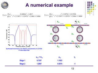
Synthesized transmission (black) and reflection (blue) characteristics
along with a Butterworth response (red) of the same order
Filter layout for 7 pole 3 zero 25 GHz asymmetric filter
Numerical example
4 5 6
1 2 3
7
]0.16340.3955][0.62470.2967][9066.00.1600[
]1.02510.0476][0.37510.3910][0.81600.266][1.04450.0902[
)1.669)(1.4)(995.1(
)(
jsjsjs
jsjsjsjs
jsjsjs
sH
−+−+−+
−+++++++
−−+
=
-30 -20 -10 0 10 20 30
-80
-60
-40
-20
0
frequency detune, ∆f (GHz)
transmission(dB)
−−
−
−
8923.0
2088.427650.2
01662.453269.35
005723.416984.58
00005104.33
2088.420004642.447966.4
02088.420002088.428923.0
Synthesized Energy coupling matrix:
To realize transmission zeros located on the imaginary axis jω, the filter requires negative
couplings between neighbour microring resonators.
To realize a negative coupling coefficient, the coupling angle between adjacent resonators
must be between 3π/2 and 2π, so that micro-racetracks with long coupling lengths are
required
g κ
RLc](https://image.slidesharecdn.com/8e6a8c38-38be-4902-8b50-031671085843-160215013746/85/PhD_seminar_final-11-320.jpg)
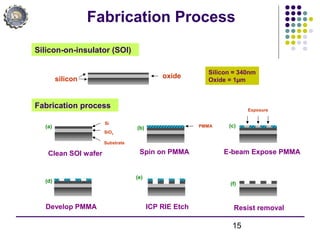
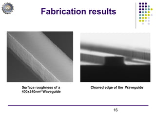
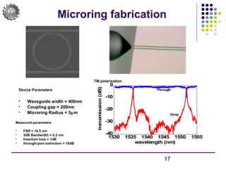
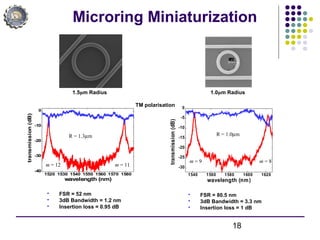


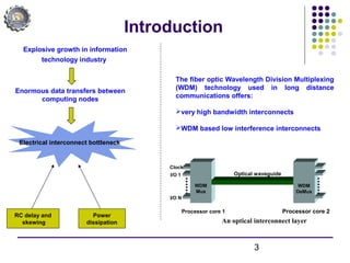
This document summarizes Ashok Prabhu Masilamani's Ph.D. presentation on advanced silicon microring resonator devices for optical signal processing. It introduces microring resonators and their use in optical filters. It outlines Masilamani's research goals to explore new coupled microring topologies that can realize complex transfer functions. The document demonstrates experimental fabrication and testing of microring filters in silicon-on-insulator material. It also shows thermal tuning of microring resonances using integrated microheaters. The research contributes new coupled microring architectures and synthesis techniques for advanced optical signal processing.