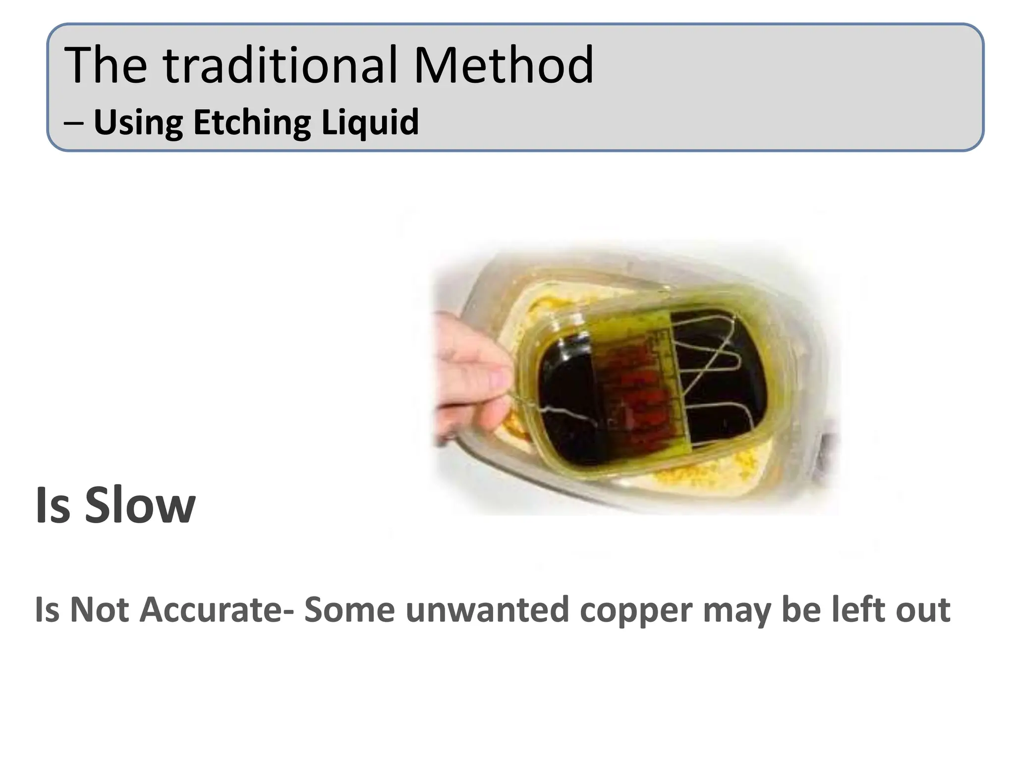
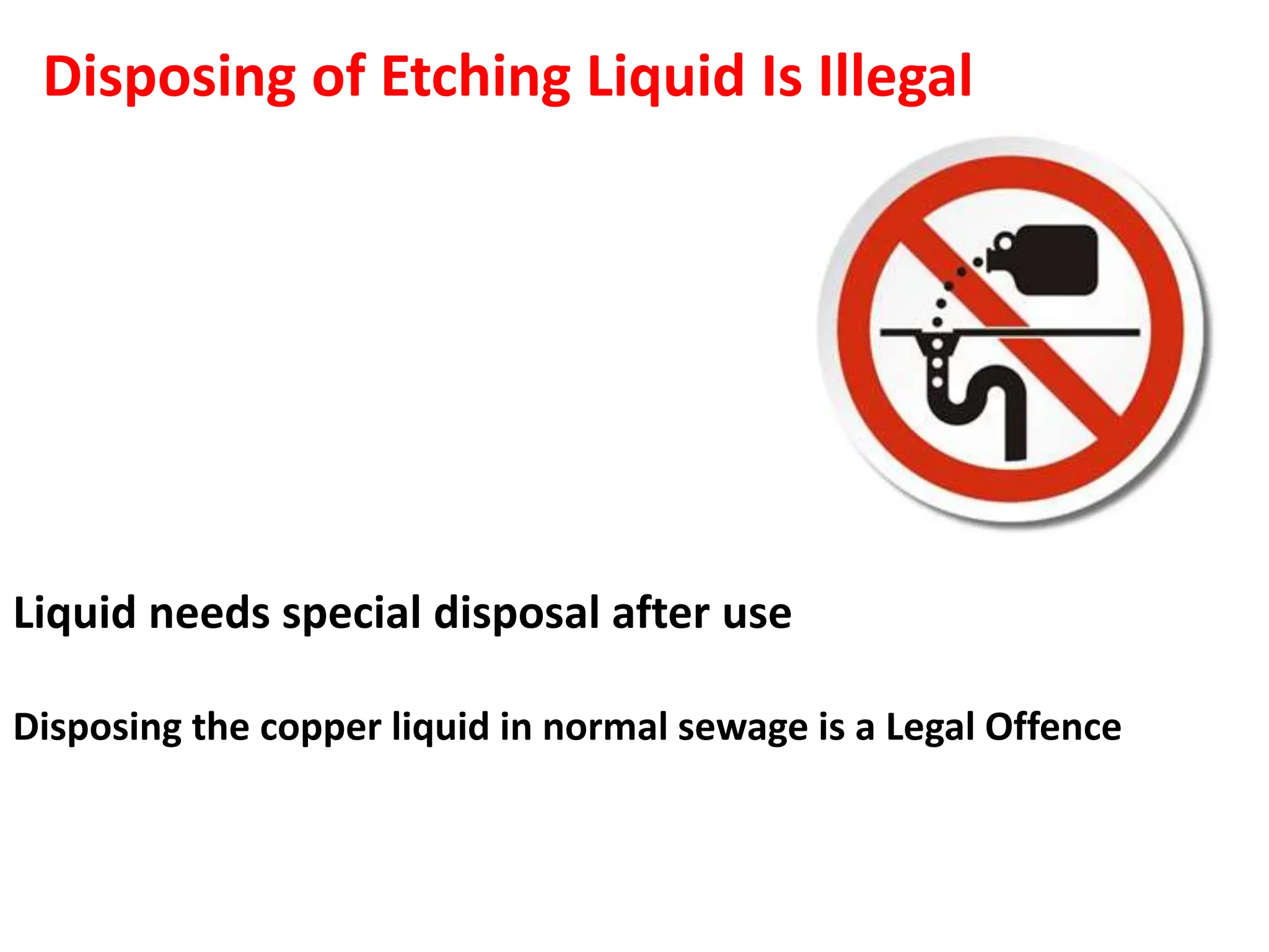
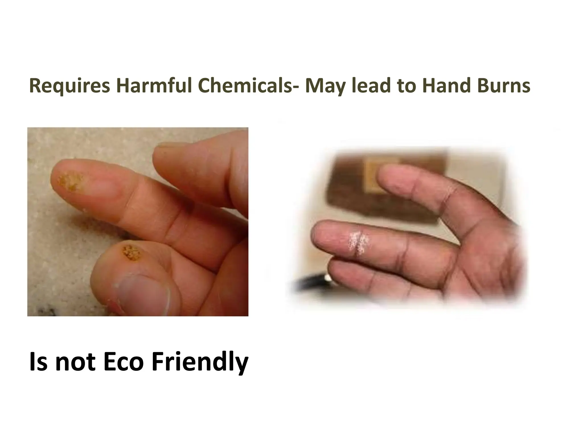
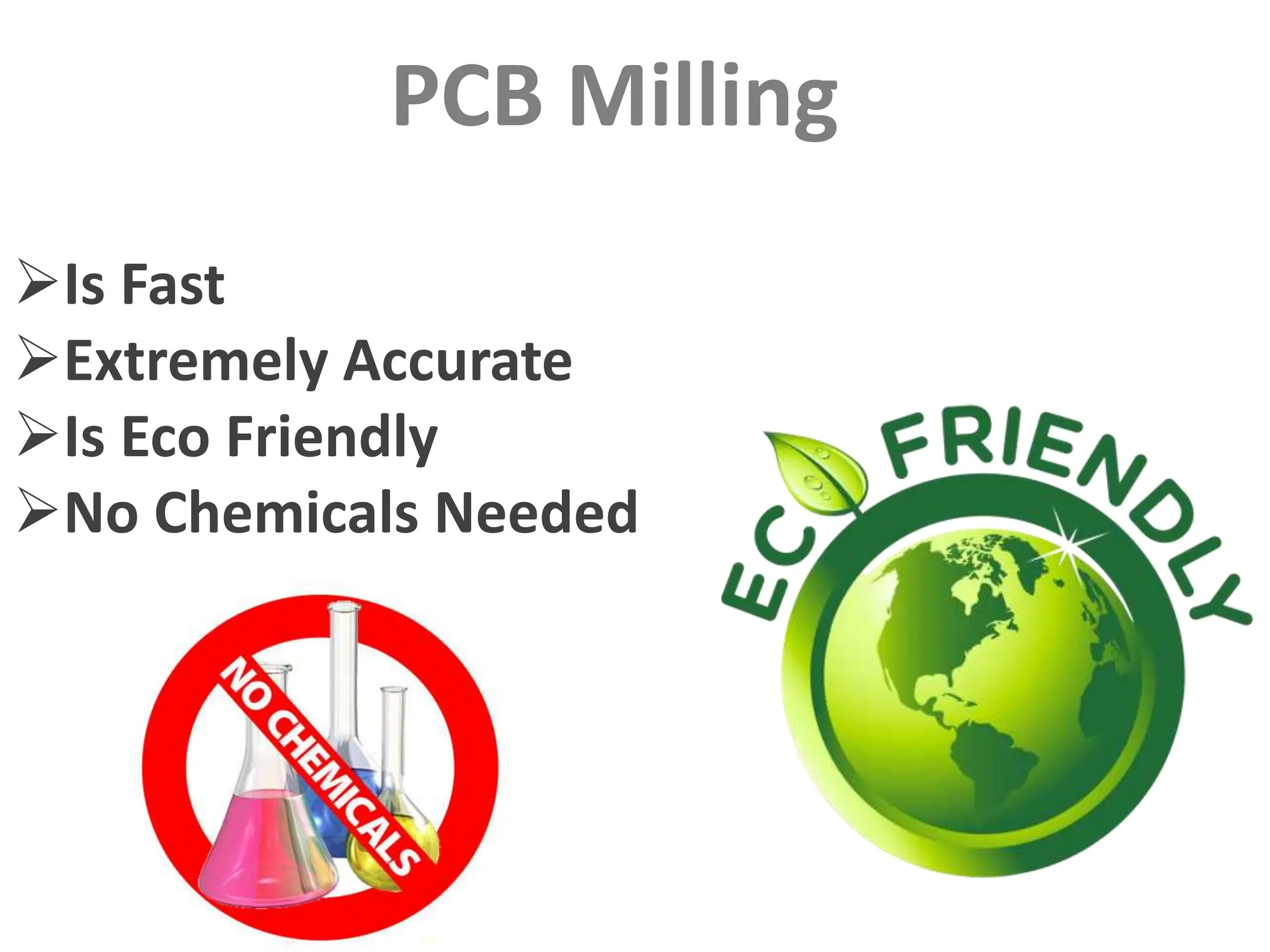
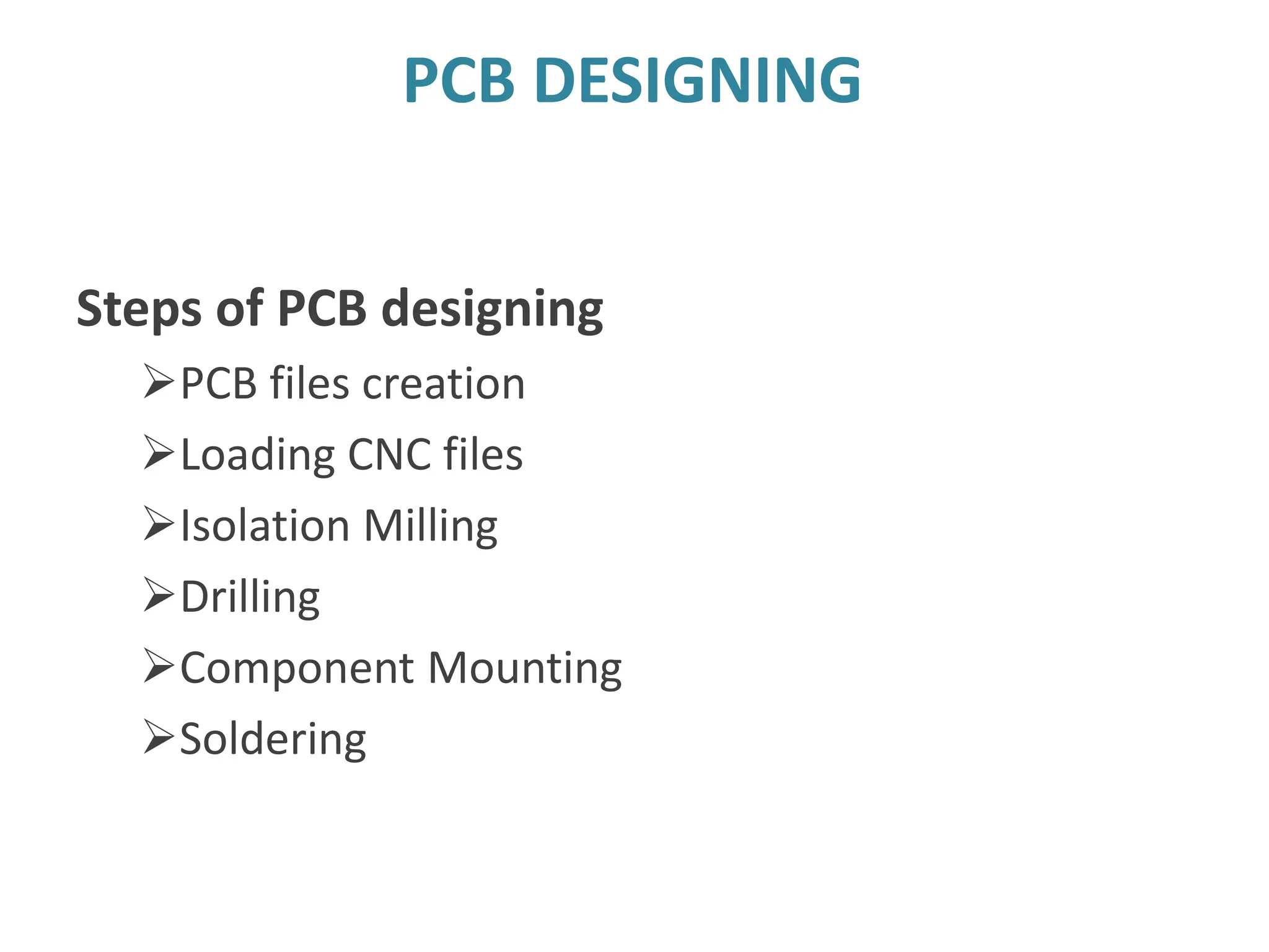
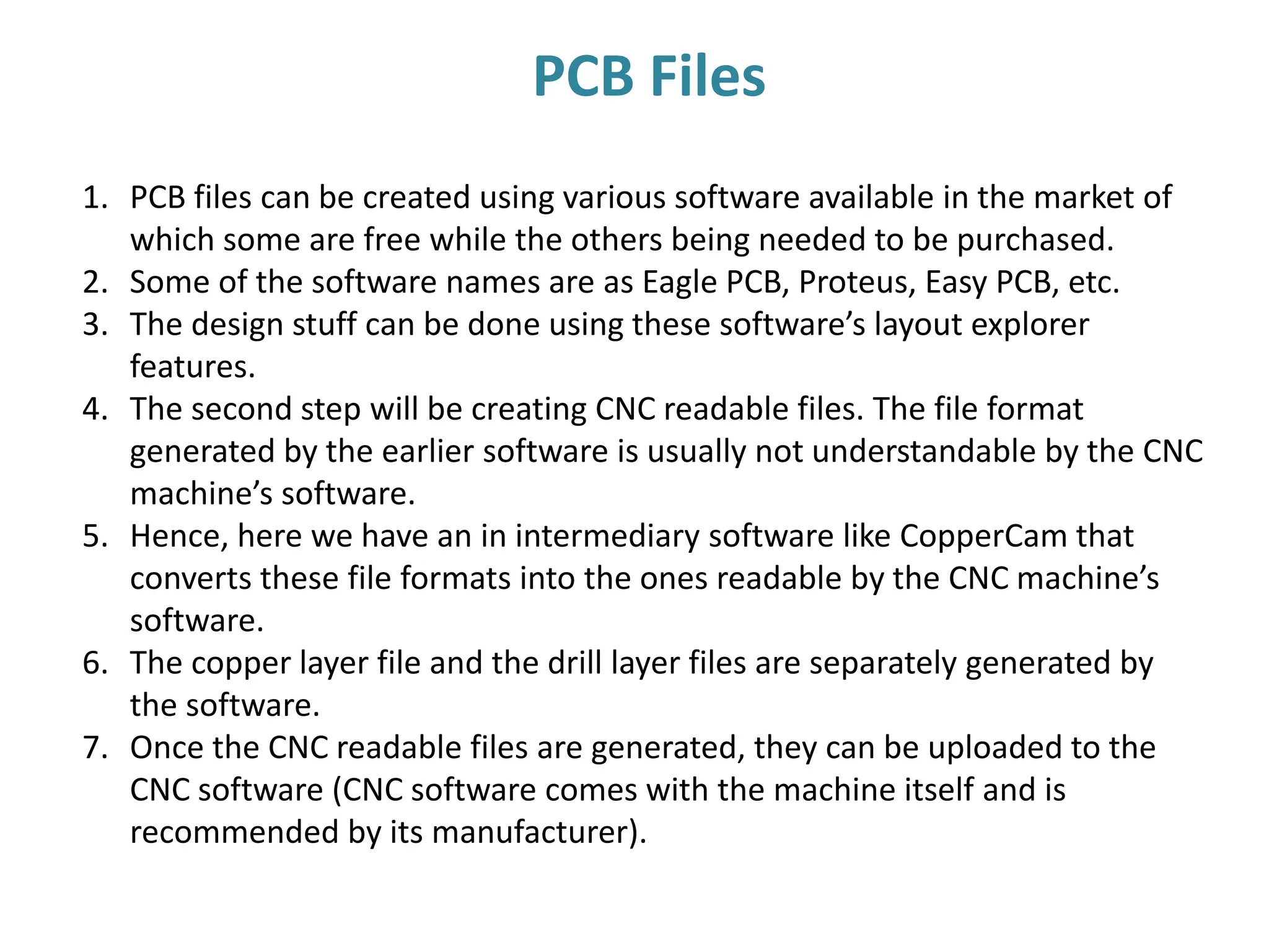
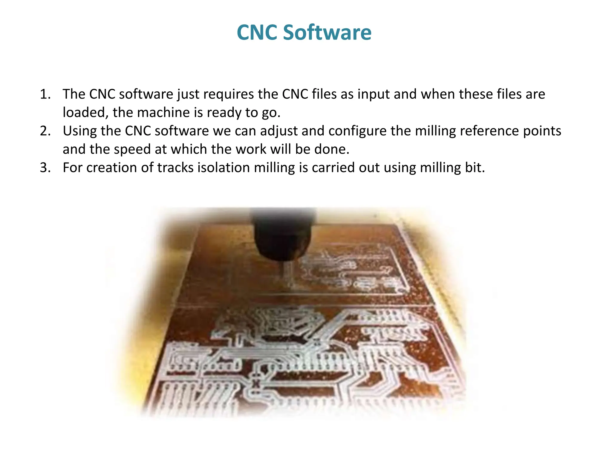
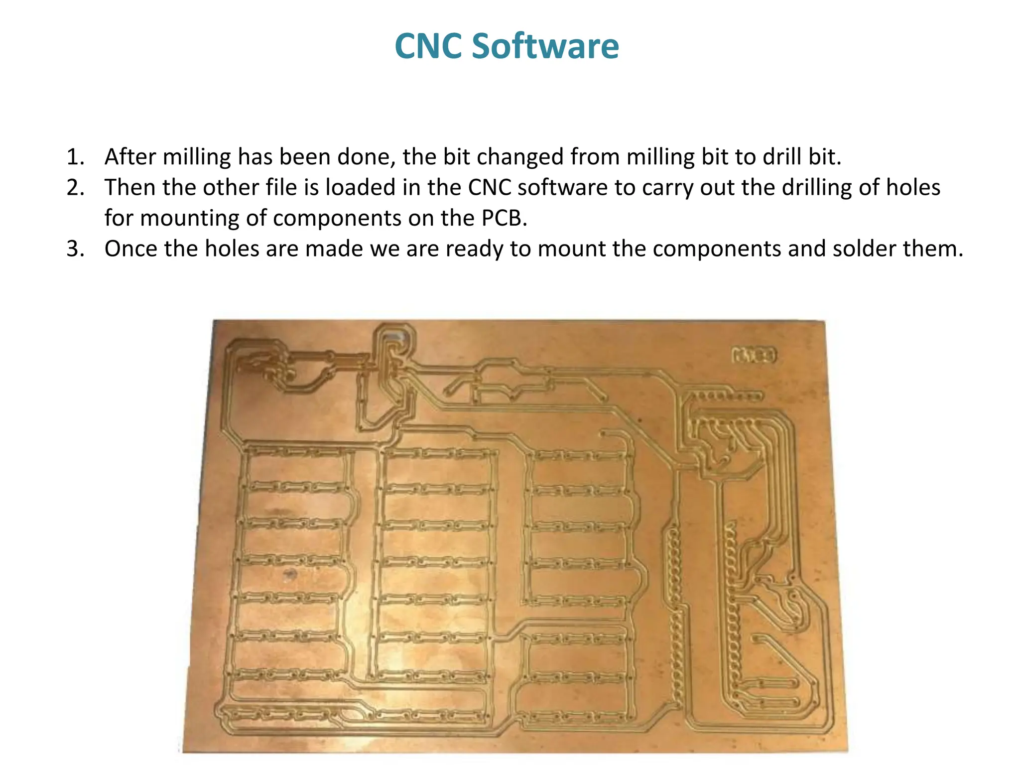
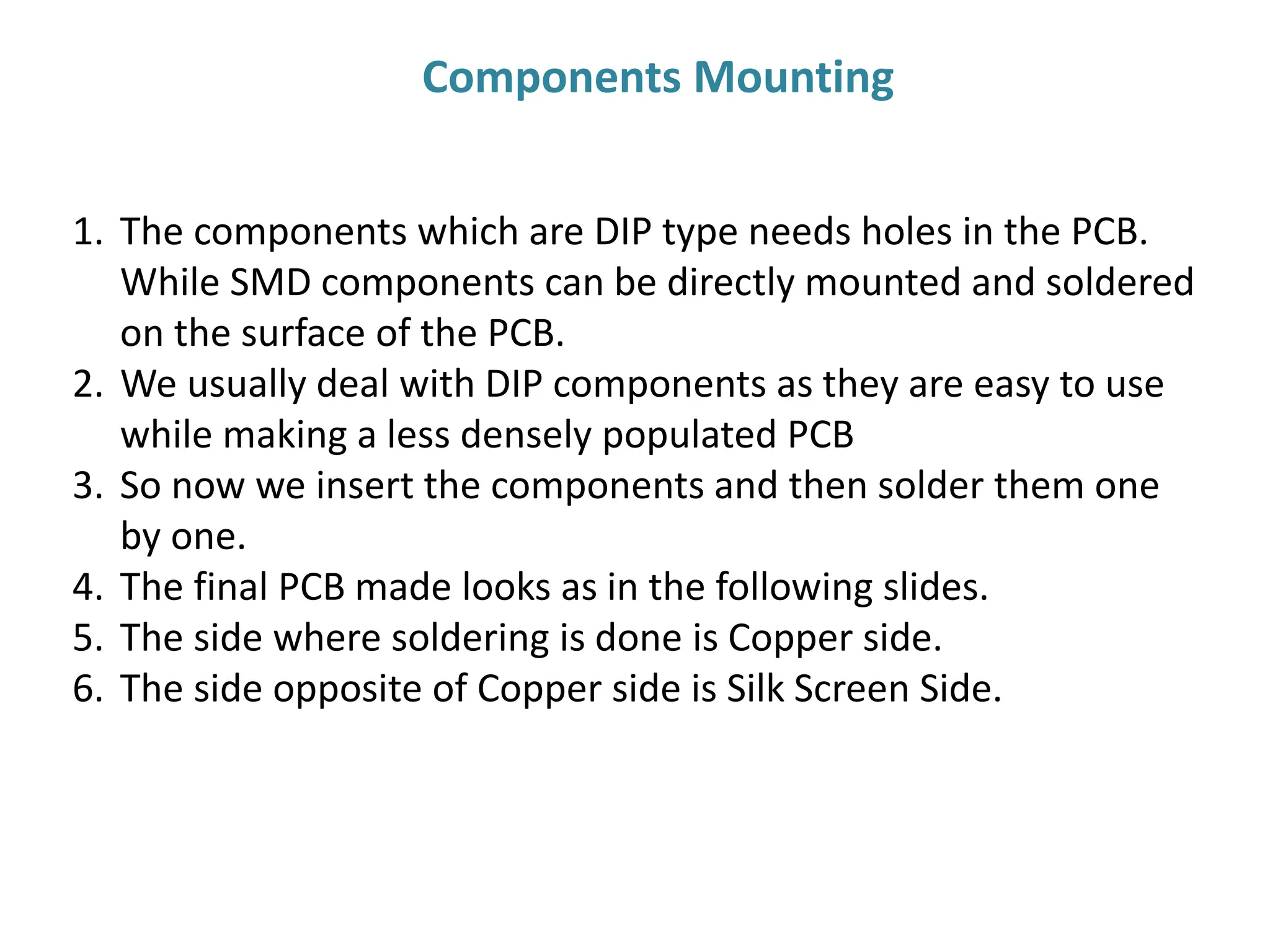
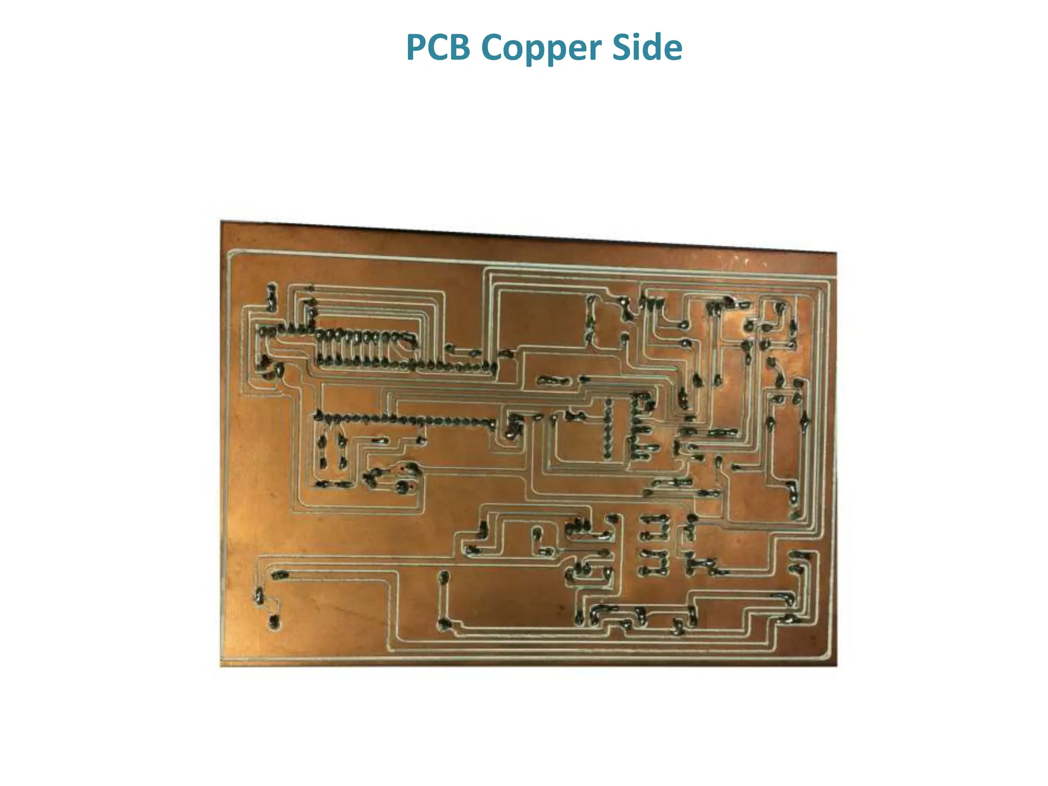
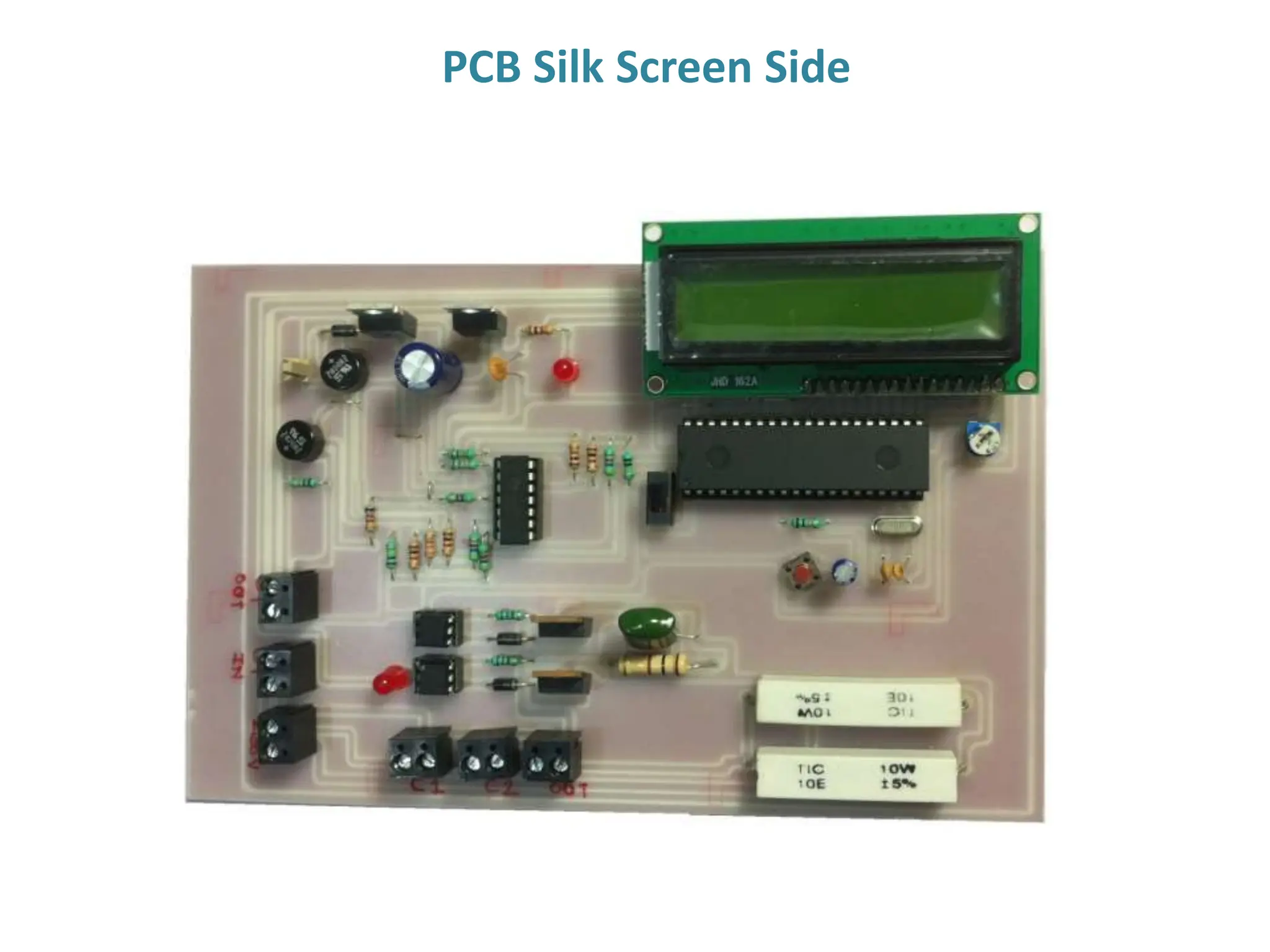
 A printed circuit board, or PCB, is what holds your
electronic components together and also gives electrical
paths for their interconnection.
 PCB boards usually have copper base for the electrical
paths known as the copper layer.
 The other side is usually fiberglass, composite epoxy, or
other laminate material that gives good mechanical
strength to the PCB.
 The components can be mounted in through hole fashion
as well as in surface mount depending upon what
component type we will use like SMD, DIP, etc.
Printed Circuit Board
The traditional Method
– Using Etching Liquid
Is Slow
Is Not Accurate- Some unwanted copper may be left out
Liquid needs special disposal after use
Disposing the copper liquid in normal sewage is a Legal Offence
Disposing of Etching Liquid Is Illegal
Requires Harmful Chemicals- May lead to Hand Burns
Is not Eco Friendly
Is Fast
Extremely Accurate
Is Eco Friendly
No Chemicals Needed
PCB Milling
Steps of PCB designing
PCB files creation
Loading CNC files
Isolation Milling
Drilling
Component Mounting
Soldering
PCB DESIGNING
1. PCB files can be created using various software available in the market of
which some are free while the others being needed to be purchased.
2. Some of the software names are as Eagle PCB, Proteus, Easy PCB, etc.
3. The design stuff can be done using these software’s layout explorer
features.
4. The second step will be creating CNC readable files. The file format
generated by the earlier software is usually not understandable by the CNC
machine’s software.
5. Hence, here we have an in intermediary software like CopperCam that
converts these file formats into the ones readable by the CNC machine’s
software.
6. The copper layer file and the drill layer files are separately generated by
the software.
7. Once the CNC readable files are generated, they can be uploaded to the
CNC software (CNC software comes with the machine itself and is
recommended by its manufacturer).
PCB Files
1. The CNC software just requires the CNC files as input and when these files are
loaded, the machine is ready to go.
2. Using the CNC software we can adjust and configure the milling reference points
and the speed at which the work will be done.
3. For creation of tracks isolation milling is carried out using milling bit.
CNC Software
1. After milling has been done, the bit changed from milling bit to drill bit.
2. Then the other file is loaded in the CNC software to carry out the drilling of holes
for mounting of components on the PCB.
3. Once the holes are made we are ready to mount the components and solder them.
CNC Software
1. The components which are DIP type needs holes in the PCB.
While SMD components can be directly mounted and soldered
on the surface of the PCB.
2. We usually deal with DIP components as they are easy to use
while making a less densely populated PCB
3. So now we insert the components and then solder them one
by one.
4. The final PCB made looks as in the following slides.
5. The side where soldering is done is Copper side.
6. The side opposite of Copper side is Silk Screen Side.
Components Mounting
PCB Copper Side
PCB Silk Screen Side
Thank You

Pcb designing and working explanation and full theory

  • 1.
     A printedcircuit board, or PCB, is what holds your electronic components together and also gives electrical paths for their interconnection.  PCB boards usually have copper base for the electrical paths known as the copper layer.  The other side is usually fiberglass, composite epoxy, or other laminate material that gives good mechanical strength to the PCB.  The components can be mounted in through hole fashion as well as in surface mount depending upon what component type we will use like SMD, DIP, etc. Printed Circuit Board
  • 2.
    The traditional Method –Using Etching Liquid Is Slow Is Not Accurate- Some unwanted copper may be left out
  • 3.
    Liquid needs specialdisposal after use Disposing the copper liquid in normal sewage is a Legal Offence Disposing of Etching Liquid Is Illegal
  • 4.
    Requires Harmful Chemicals-May lead to Hand Burns Is not Eco Friendly
  • 6.
    Is Fast Extremely Accurate IsEco Friendly No Chemicals Needed PCB Milling
  • 7.
    Steps of PCBdesigning PCB files creation Loading CNC files Isolation Milling Drilling Component Mounting Soldering PCB DESIGNING
  • 8.
    1. PCB filescan be created using various software available in the market of which some are free while the others being needed to be purchased. 2. Some of the software names are as Eagle PCB, Proteus, Easy PCB, etc. 3. The design stuff can be done using these software’s layout explorer features. 4. The second step will be creating CNC readable files. The file format generated by the earlier software is usually not understandable by the CNC machine’s software. 5. Hence, here we have an in intermediary software like CopperCam that converts these file formats into the ones readable by the CNC machine’s software. 6. The copper layer file and the drill layer files are separately generated by the software. 7. Once the CNC readable files are generated, they can be uploaded to the CNC software (CNC software comes with the machine itself and is recommended by its manufacturer). PCB Files
  • 9.
    1. The CNCsoftware just requires the CNC files as input and when these files are loaded, the machine is ready to go. 2. Using the CNC software we can adjust and configure the milling reference points and the speed at which the work will be done. 3. For creation of tracks isolation milling is carried out using milling bit. CNC Software
  • 10.
    1. After millinghas been done, the bit changed from milling bit to drill bit. 2. Then the other file is loaded in the CNC software to carry out the drilling of holes for mounting of components on the PCB. 3. Once the holes are made we are ready to mount the components and solder them. CNC Software
  • 11.
    1. The componentswhich are DIP type needs holes in the PCB. While SMD components can be directly mounted and soldered on the surface of the PCB. 2. We usually deal with DIP components as they are easy to use while making a less densely populated PCB 3. So now we insert the components and then solder them one by one. 4. The final PCB made looks as in the following slides. 5. The side where soldering is done is Copper side. 6. The side opposite of Copper side is Silk Screen Side. Components Mounting
  • 12.
  • 13.
  • 14.