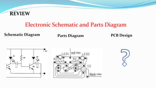
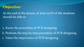
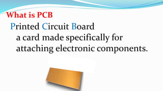
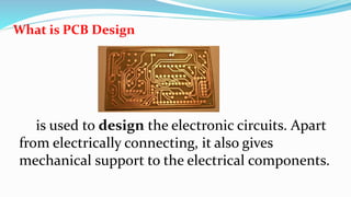
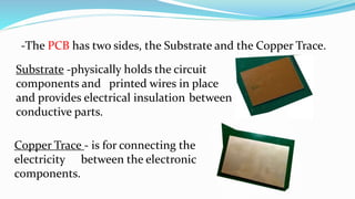
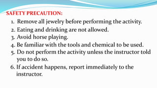
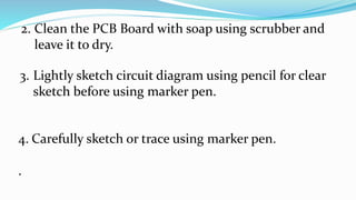
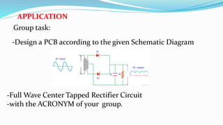
EPAS 12
Maragusan National High School
Compostela Valley Province
REVIEW
Electronic Schematic and Parts Diagram
Schematic Diagram Parts Diagram PCB Design
DESIGN
Objective:
At the end of the lesson, at least 100% of the students
should be able to
a. Know the procedure of PCB designing
b. Perform the step by step procedure of PCB designing
c. Value the importance of PCB designing
PCB DESIGNING
What is PCB
Printed Circuit Board
a card made specifically for
attaching electronic components.
What is PCB Design
is used to design the electronic circuits. Apart
from electrically connecting, it also gives
mechanical support to the electrical components.
PCB serves two purpose
1. It is a place to Mount Components
2. It Provides the means of electrical
Component
-The PCB has two sides, the Substrate and the Copper Trace.
Copper Trace - is for connecting the
electricity between the electronic
components.
Substrate -physically holds the circuit
components and printed wires in place
and provides electrical insulation between
conductive parts.
SAFETY PRECAUTION:
6. If accident happens, report immediately to the
instructor.
1. Remove all jewelry before performing the activity.
2. Eating and drinking are not allowed.
3. Avoid horse playing.
4. Be familiar with the tools and chemical to be used.
5. Do not perform the activity unless the instructor told
you to do so.
STEPS IN PCB DESIGNING:
1. Prepare the materials needed, we will be using
Permanent Marker, PCB, Ferric Chloride, Plastic
Container, Plastic Clip, Soap, Spongy Scrubber.
2. Clean the PCB Board with soap using scrubber and
leave it to dry.
3. Lightly sketch circuit diagram using pencil for clear
sketch before using marker pen.
4. Carefully sketch or trace using marker pen.
.
5. Subject to Etching Process.
For the etching process, put enough amount of ferric
chloride to the container to submerge the PCB.
Usually the etching process takes 5-15 mins.
Etching is traditionally the process of using strong acid or
mordant to cut into the unprotected parts of a metal
surface to create a design in the metal. In modern
manufacturing, other chemicals may be used on other
types of material.
5. Subject to Etching Process.
For the etching process, put enough amount of ferric
chloride to the container to submerge the PCB.
Usually the etching process takes 5-15 mins.
6. Rinse the PCB with water.
7. Using thinner, remove marker lines on the PCB
board.
APPLICATION
Group task:
-Design a PCB according to the given Schematic Diagram
-Full Wave Center Tapped Rectifier Circuit
-with the ACRONYM of your group.
Direction: Read the following questions and write your answers in a ½ crosswise
size of a paper.
I. Identification
________1. It is the backbone of electronic devices.
________2. It provides the electrical needs of the electronic
components.
________3. It holds and provide insulation to the electronic
components.
II. Enumeration
4-10 7 steps in PCB designing
Assignment
1. Research about different PBC design.
2. Each group will submit a PCB with holes and make it sure
that it is already drilled.

Pcb design demo final na jud

  • 1.
    EPAS 12 Maragusan NationalHigh School Compostela Valley Province
  • 2.
    REVIEW Electronic Schematic andParts Diagram Schematic Diagram Parts Diagram PCB Design
  • 3.
  • 4.
    Objective: At the endof the lesson, at least 100% of the students should be able to a. Know the procedure of PCB designing b. Perform the step by step procedure of PCB designing c. Value the importance of PCB designing
  • 5.
  • 6.
    What is PCB PrintedCircuit Board a card made specifically for attaching electronic components.
  • 7.
    What is PCBDesign is used to design the electronic circuits. Apart from electrically connecting, it also gives mechanical support to the electrical components.
  • 8.
    PCB serves twopurpose 1. It is a place to Mount Components 2. It Provides the means of electrical Component
  • 9.
    -The PCB hastwo sides, the Substrate and the Copper Trace. Copper Trace - is for connecting the electricity between the electronic components. Substrate -physically holds the circuit components and printed wires in place and provides electrical insulation between conductive parts.
  • 10.
    SAFETY PRECAUTION: 6. Ifaccident happens, report immediately to the instructor. 1. Remove all jewelry before performing the activity. 2. Eating and drinking are not allowed. 3. Avoid horse playing. 4. Be familiar with the tools and chemical to be used. 5. Do not perform the activity unless the instructor told you to do so.
  • 11.
    STEPS IN PCBDESIGNING: 1. Prepare the materials needed, we will be using Permanent Marker, PCB, Ferric Chloride, Plastic Container, Plastic Clip, Soap, Spongy Scrubber.
  • 12.
    2. Clean thePCB Board with soap using scrubber and leave it to dry. 3. Lightly sketch circuit diagram using pencil for clear sketch before using marker pen. 4. Carefully sketch or trace using marker pen. .
  • 13.
    5. Subject toEtching Process. For the etching process, put enough amount of ferric chloride to the container to submerge the PCB. Usually the etching process takes 5-15 mins. Etching is traditionally the process of using strong acid or mordant to cut into the unprotected parts of a metal surface to create a design in the metal. In modern manufacturing, other chemicals may be used on other types of material.
  • 14.
    5. Subject toEtching Process. For the etching process, put enough amount of ferric chloride to the container to submerge the PCB. Usually the etching process takes 5-15 mins. 6. Rinse the PCB with water. 7. Using thinner, remove marker lines on the PCB board.
  • 15.
    APPLICATION Group task: -Design aPCB according to the given Schematic Diagram -Full Wave Center Tapped Rectifier Circuit -with the ACRONYM of your group.
  • 16.
    Direction: Read thefollowing questions and write your answers in a ½ crosswise size of a paper. I. Identification ________1. It is the backbone of electronic devices. ________2. It provides the electrical needs of the electronic components. ________3. It holds and provide insulation to the electronic components. II. Enumeration 4-10 7 steps in PCB designing
  • 17.
    Assignment 1. Research aboutdifferent PBC design. 2. Each group will submit a PCB with holes and make it sure that it is already drilled.