
Recommended
More Related Content
What's hot
What's hot (20)
Similar to Past Research and Achievements in SiC Semiconductors for Power Devices
Similar to Past Research and Achievements in SiC Semiconductors for Power Devices (20)
Past Research and Achievements in SiC Semiconductors for Power Devices
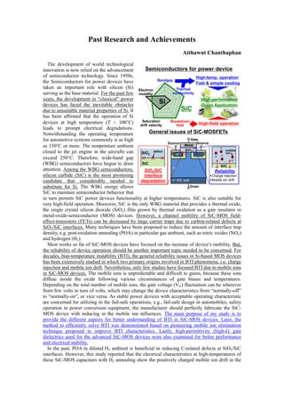
- 1. Past Research and Achievements Atthawut Chanthaphan The development of world technological innovation is now relied on the advancement of semiconductor technology. Since 1950s, the Semiconductors for power devices have taken an important role with silicon (Si) serving as the base material. For the past few years, the development in “classical” power devices has faced the inevitable obstacles due to unsuitable material properties of Si. It has been affirmed that the operation of Si devices at high temperature (T > 100C) leads to prompt electrical degradations. Notwithstanding the operating temperature for automotive systems commonly is as high as 150C or more. The temperature ambient closed to the jet engine in the aircrafts can exceed 250C. Therefore, wide-band gap (WBG) semiconductors have begun to draw attention. Among the WBG semiconductors, silicon carbide (SiC) is the most promising candidate that considerably needed to substitute for Si. The WBG energy allows SiC to maintain semiconductor behavior that in turn permits SiC power devices functionality at higher temperatures. SiC is also suitable for very high-field operation. Moreover, SiC is the only WBG material that provides a thermal oxide, the single crystal silicon dioxide (SiO2) film grown by thermal oxidation as a gate insulator in metal-oxide-semiconductor (MOS) devices. However, a channel mobility of SiC-MOS field- effect-transistors (FETs) can be decreased by large carrier traps due to carbon-related defects at SiO2/SiC interfaces. Many techniques have been proposed to reduce the amount of interface trap density, e.g. post-oxidation annealing (POA) in particular gas ambient, such as nitric oxides (NOx) and hydrogen (H2). Most works so far of SiC-MOS devices have focused on the increase of device’s mobility. But, the reliability of device operation should be another important topic needed to be concerned. For decades, bias-temperature instability (BTI), the general reliability issues in Si-based MOS devices has been extensively studied in which two primary origins involved in BTI phenomena, i.e. charge injection and mobile ion drift. Nevertheless, only few studies have focused BTI due to mobile ions in SiC-MOS devices. The mobile ions is unpredictable and difficult to guess, because these ions diffuse inside the oxide following various circumstances of gate biases and temperatures. Depending on the total number of mobile ions, the gate voltage (VG) fluctuation can be wherever from few volts to tens of volts, which may change the device characteristics from “normally-off” to “normally-on”, or vice versa. As stable power devices with acceptable operating characteristic are concerned for utilizing in the fail-safe operations, e.g., fail-safe design in automobiles, safety operation in power conversion equipment, the manufacturer should perfectly fabricate the SiC- MOS device with reducing in the mobile ion influences. The main purpose of my study is to provide the different aspects for better understanding of BTI in SiC-MOS devices. Later, the method to efficiently solve BTI was demonstrated based on pioneering mobile ion elimination technique proposed to improve BTI characteristics. Lastly, high-permittivity (high-k) gate dielectrics used for the advanced SiC-MOS devices were also examined for better performance and electrical stability. In the past, POA in diluted H2 ambient is beneficial in reducing C-related defects at SiO2/SiC interfaces. However, this study reported that the electrical characteristics at high-temperatures of these SiC-MOS capacitors with H2 annealing show the positively charged mobile ion drift in the Bandgap Thermal conductivity Breakdown field Saturation drift velocity Electron mobility SiC Semiconductors for power device High-field operation Si High-performance Green Application High-temp. operation Fast & simple cooling p n+-SiC sub n+p Metal n- Gate Drain SiC + + + + Charge injection Mobile ion drift Reliability SiO2 SourceSource e- e- SiO2/SiC interface degradation SiO2 SiC defect mobile ion General issues of SiC-MOSFETs
- 2. oxides. The results were also compared with Si-MOS capacitors, but mobile ions were not observed in any fabricated Si-MOS capacitor. Thus, common ion contaminations (i.e. Na+ , K+ ) are ruled out to indicate an intrinsic problem of SiC. Moreover, it is found that these mobile ions intensely degrade the quality of SiO2/SiC interfaces, which may further reduce the performance of SiC-MOSFETs. In order to obtain mobile ion-free SiC-MOS devices, the mobile ion elimination was proposed based on the bias-temperature stress (BTS) and subsequent etching of a few nm-thick SiO2 to reject the mobile ions. By using this method, mobile ions were eliminated completely while maintaining the good interface property attributed to H2 annealing. Furthermore, diffusivity of the mobile ions inherent to SiC-MOS devices was also investigated in high-k aluminum oxynitride (AlON) gate dielectrics. Significant improvement of BTI characteristics in SiC-MOS devices was demonstrated with AlON dielectrics deposited on thin thermal oxides. AlON/SiO2 stacked dielectrics were found to be beneficial not only for reducing gate leakage current but also for suppressing diffusion of mobile ions, leading to stable SiC-MOS characteristics even under strong electric fields and high temperatures. Reference Journal papers (as corresponding author): 1. A. Chanthaphan, T. Hosoi, Y. Nakano, T. Nakamura, T. Shimura, and H. Watanabe, Improved bias-temperature instability characteristics in SiC metal-oxide-semiconductor devices with aluminum oxynitride dielectrics, Applied Physics Letters, Vol. 104, No.12, pp.122105, month, 2014. 2. A. Chanthaphan, T. Hosoi, Y. Nakano, T. Nakamura, T. Shimura, and H. Watanabe, Degradation of SiO2/SiC interface properties due to mobile ions intrinsically generated by high-temperature hydrogen annealing," Material Science Forum, Vol. 778-780, pp.541-544, month, 2014. 3. A. Chanthaphan, T. Hosoi, Y. Nakano, T. Nakamura, T. Shimura, and H. Watanabe, Understanding and controlling bias-temperature instability in SiC metal-oxide-semiconductor devices induced by unusual generation of mobile ions, Applied Physics Letter, Vol. 102, No. 9, pp.093510, month, 2013. Summary of past research 3. Elimination of mobile ion by BTS** 4. Stability improved by AlON on thin SiO2**** SiC metal + + + + + + SiC metal oxide (SiO2) defects Poor interface quality of SiC-MOS devices • Defects at SiO2/SiC interface • Low mobility of MOSFETs • Better interface but mobile ion generation • Instability of MOSFETs 1. Mobile ion generation by H2 annealing* H2 annealing SiC + + + oxide (SiO2) oxide etch • BTS with oxide etch • Good interface without mobile ions SiC Aluminum oxynitride (AlON) • AlON suppressed mobile ion diffusion • More stable MOSFETs • Passivation of Interface defect SiC metal + + + • Mobile ions located at SiO2/SiC interface increase defect states 2. Mobile ion related interface degradation*** Move mobile ion to SiO2/SiC interface • Bias-temperature stress (BTS) Journal publications *A. Chanthaphan et al., Appl. Phys. Lett. 100, 252103 (2012) **A. Chanthaphan et al., Appl. Phys. Lett. 102, 093510 (2013). ***A. Chanthaphan et al., Mater. Sci. Forum 778-780, 541 (2014). ****A. Chanthaphan et al., Appl. Phys. Lett. 104, 122105 (2014). oxide (SiO2)
- 3. 4. A. Chanthaphan, T. Hosoi, S. Mitani, Y. Nakano, T. Nakamura, T. Shimura, and H. Watanabe, Investigation of unusual mobile ion effects in thermally grown SiO2 on 4H-SiC(0001) at high temperatures, Applied Physics Letter, Vol. 100, No. 25, pp.252103, month, 2012. Journal papers (as contributing author): 1. H. Watanabe, T. Hosoi, T. Kirino, Y. Uenishi, A. Chanthaphan, A. Yoshigoe, Y. Teraoka, S. Mitani, Y. Nakano, T. Nakamura, and T. Shimura, Synchrotron radiation photoelectron spectroscopy study of thermally grown oxides on 4H-SiC(0001) Si-face and (000-1) C-face substrates, Material Science Forum, Vol. 717-720, pp.697-702, month, 2012. 2. T. Hosoi, T. Kirino, A. Chanthaphan, Y. Uenishi, D. Ikeguchi, A. Yoshigoe, Y. Teraoka, S. Mitani, Y. Nakano, T. Nakamura, T. Shimura, and H. Watanabe, Impact of interface defect passivation on conduction band offset at SiO2/4H-SiC Interface, Material Science Forum, Vol. 717-720, pp.721-724, month, 2012. 3. H. Watanabe, T. Hosoi, T. Kirino, Y. Uenishi, A. Chanthaphan, D. Ikeguchi, A. Yoshigoe, Y. Teraoka, S. Mitani, Y. Nakano, T. Nakamura, and T. Shimura, Gate stack technologies for SiC power MOSFETs, ECS Transactions, Vol. 41, No. 3, pp.77-90, month, 2011. 4. H. Watanabe, T. Hosoi, T. Kirino, Y. Kagei, Y. Uenishi, A. Chanthaphan, A. Yoshigoe, Y. Teraoka, and T. Shimura, Synchrotron x-ray photoelectron spectroscopy study on thermally grown SiO2/4H-SiC(0001) interface and its correlation with electrical properties, Applied Physics Letter, Vol. 99, No. 2, pp.021907, month, 2011. 5. H. Watanabe, T. Kirino, Y. Uenishi, A. Chanthaphan, A. Yoshigoe, Y. Teraoka, S. Mitani, Y. Nakano, T. Nakamura, T. Hosoi and T. Shimura,"Impact of stacked AlON/SiO2 gate dielectrics for SiC power devices, ECS Transactions, Vol. 35, No. 2, pp.265-274, month, 2011. International conferences (as corresponding author): 1. A. Chanthaphan, Y. Nakano, T. Nakamura, T. Hosoi, T. Shimura, and H. Watanabe, Bias- temperature instability of SiC-MOS devices induced by unusual generation of mobile ions in thermal oxides, International Workshop on Atomically Controlled Fabrication Technology, p.15, (Nakanoshima Center, Osaka University, Osaka, Japan, February 5-6, 2014). 2. A. Chanthaphan, T. Hosoi, Y. Nakano, T. Nakamura, T. Shimura, and H. Watanabe, Suppression of mobile ion diffusion with AlON/SiO2 stacked gate dielectrics for improving bias-temperature instability in SiC-MOS devices, International Conference on Silicon Carbide and Related Materials 2013 (ICSCRM2013), We-P-62, (Phoenix Seagaia Resort, Miyazaki, Japan, September 29 - October 4, 2013). 3. A. Chanthaphan, T. Hosoi, Y. Nakano, T. Nakamura, T. Shimura, and H. Watanabe, Degradation of SiO2/SiC interface properties due to mobile ions intrinsically generated by high-temperature hydrogen annealing, International Conference on Silicon Carbide and Related Materials 2013 (ICSCRM2013), Tu-P-39, (Phoenix Seagaia Resort, Miyazaki, Japan, September 29 - October 4, 2013). 4. A. Chanthaphan, T. Kirino, Y. Uenishi, D. Ikeguchi, S. Mitani, Y. Nakano, T. Nakamura, T. Hosoi, T. Shimura, and H. Watanabe, Insight into bias-temperature instability of 4H-SiC MOS devices with thermally grown SiO2 dielectrics," 2012 MRS Spring Meeting, H5.6, (San Francisco, CA, USA, April 11, 2012). 5. A. Chanthaphan, S. Mitani, Y. Nakano, T. Nakamura, T. Hosoi, T. Shimura and H. Watanabe, Elimination of mobile ions in thermal oxide of SiC MOS devices, Extended Abstract of Fifth International Symposium on Atomically Controlled Fabrication Technology, pp.60-61, (Osaka University Nakanoshima Center, Osaka, Japan, October 22-24, 2012). 6. A. Chanthaphan, T. Kirino, Y. Uenishi, D. Ikeguchi, S. Mitani, Y. Nakano, T. Nakamura, T. Hosoi, T. Shimura, and H. Watanabe, Flatband voltage instability due to mobile ions in 4H- SiC metal-oxide-semiconductor devices, Extended Abstract of Fourth International Symposium on Atomically Controlled Fabrication Technology, pp.248-249, (Osaka University Nakanoshima Center, Osaka, Japan, October 31, 2011 - November 02, 2011).