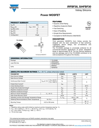
Original Power MOSFET IRFBF30 IRFBF30PBF 900V 3.6A New Vishay Siliconix
https://authelectronic.com/original-power-mosfet-irfbf30-irfbf30pbf-900v-3-6a-new-vishay-siliconix
Original Power MOSFET IRFP460PBF IRFP460 460 500V 20A TO-247 New Vishay Silic...AUTHELECTRONIC
Original Power MOSFET IRFP460PBF IRFP460 460 500V 20A TO-247 New Vishay Siliconix
https://authelectronic.com/original-power-mosfet-irfp460pbf-irfp460-460-500v-20a-to-247-new-vishay-siliconix
Original Power MOSFET IRFP460PBF IRFP460 460 500V 20A TO-247 New Vishay Silic...AUTHELECTRONIC
Original Power MOSFET IRFP460PBF IRFP460 460 500V 20A TO-247 New Vishay Siliconix
https://authelectronic.com/original-power-mosfet-irfp460pbf-irfp460-460-500v-20a-to-247-new-vishay-siliconix
Original P-CHANNEL POWER MOSFETS IRFP9240PBF IRFP9240 9240 200V 12A TO-247 NewAUTHELECTRONIC
Original P-CHANNEL POWER MOSFETS IRFP9240PBF IRFP9240 9240 200V 12A TO-247 New
https://authelectronic.com/original-p-channel-power-mosfets-irfp9240pbf-irfp9240-9240-200v-12a-to-247-new
Original P-CHANNEL MOSFET IRF5210PBF IRF5210 5210 100V 38A TO-220 New IRAUTHELECTRONIC
Original P-CHANNEL MOSFET IRF5210PBF IRF5210 5210 100V 38A TO-220 New IR
https://authelectronic.com/original-p-channel-mosfet-irf5210pbf-irf5210-5210-100v-38a-to-220-new-ir
Original Power MOSFET IRFP240 IRFP240PBF 240 200V 20A TO-247 New Vishay Silic...AUTHELECTRONIC
Original Power MOSFET IRFP240 IRFP240PBF 240 200V 20A TO-247 New Vishay Siliconix
https://authelectronic.com/original-power-mosfet-irfp240-irfp240pbf-240-200v-20a-to-247-new-vishay-siliconix
Original Mosfet 047N08 FDP047N08 47N08 75V TO-220 New FairchildAUTHELECTRONIC
Original Mosfet 047N08 FDP047N08 47N08 75V TO-220 New Fairchild
https://authelectronic.com/original-mosfet-047n08-fdp047n08-47n08-75v-to-220-new-fairchild
Original N Channel Mosfet IRF3710PBF IRF3710 3710 37A 100V NewAUTHELECTRONIC
Original N Channel Mosfet IRF3710PBF IRF3710 3710 37A 100V New
https://authelectronic.com/original-n-channel-mosfet-irf3710pbf-irf3710-3710-37a-100v-new
Original N-Channel Mosfet IRFUC20PBF 600V 2A TO-251 New VishayAUTHELECTRONIC
Original N-Channel Mosfet IRFUC20PBF 600V 2A TO-251 New Vishay
https://authelectronic.com/original-n-channel-mosfet-irfuc20pbf-600v-2a-to-251-new-vishay
Original P-Channel Mosfet NTD2955T4G 2955G 2955 60V 12A TO-252 New On Semico...AUTHELECTRONIC
Original P-Channel Mosfet NTD2955T4G 2955G 2955 60V 12A TO-252 New On Semiconductor
https://authelectronic.com/original-p-channel-mosfet-ntd2955t4g-2955g-2955-60v-12a-to-252-new-on-semiconductor
Original P Channel Mosfet IRF9Z34 IRF9Z34N IRF9Z34NPBF 9Z34 60V 18A TO 220 NewAUTHELECTRONIC
Original P Channel Mosfet IRF9Z34 IRF9Z34N IRF9Z34NPBF 9Z34 60V 18A TO 220 New
https://authelectronic.com/original-p-channel-mosfet-irf9z34-irf9z34n-irf9z34npbf-9z34-60v-18a-to-220-new
Original Mosfet IRF4905PBF IRF4905 IRF4905 4905 55V 74A TO-220 New Internatio...AUTHELECTRONIC
Original Mosfet IRF4905PBF IRF4905 IRF4905 4905 55V 74A TO-220 New International Rectifier
https://authelectronic.com/original-mosfet-irf4905pbf-irf4905-irf4905-4905-55v-74a-to-220-new-international-rectifier
Similar to Original Power MOSFET IRFBF30 IRFBF30PBF 900V 3.6A New Vishay Siliconix (13)
Hybrid optimization of pumped hydro system and solar- Engr. Abdul-Azeez.pdffxintegritypublishin
Advancements in technology unveil a myriad of electrical and electronic breakthroughs geared towards efficiently harnessing limited resources to meet human energy demands. The optimization of hybrid solar PV panels and pumped hydro energy supply systems plays a pivotal role in utilizing natural resources effectively. This initiative not only benefits humanity but also fosters environmental sustainability. The study investigated the design optimization of these hybrid systems, focusing on understanding solar radiation patterns, identifying geographical influences on solar radiation, formulating a mathematical model for system optimization, and determining the optimal configuration of PV panels and pumped hydro storage. Through a comparative analysis approach and eight weeks of data collection, the study addressed key research questions related to solar radiation patterns and optimal system design. The findings highlighted regions with heightened solar radiation levels, showcasing substantial potential for power generation and emphasizing the system's efficiency. Optimizing system design significantly boosted power generation, promoted renewable energy utilization, and enhanced energy storage capacity. The study underscored the benefits of optimizing hybrid solar PV panels and pumped hydro energy supply systems for sustainable energy usage. Optimizing the design of solar PV panels and pumped hydro energy supply systems as examined across diverse climatic conditions in a developing country, not only enhances power generation but also improves the integration of renewable energy sources and boosts energy storage capacities, particularly beneficial for less economically prosperous regions. Additionally, the study provides valuable insights for advancing energy research in economically viable areas. Recommendations included conducting site-specific assessments, utilizing advanced modeling tools, implementing regular maintenance protocols, and enhancing communication among system components.
About
Indigenized remote control interface card suitable for MAFI system CCR equipment. Compatible for IDM8000 CCR. Backplane mounted serial and TCP/Ethernet communication module for CCR remote access. IDM 8000 CCR remote control on serial and TCP protocol.
• Remote control: Parallel or serial interface.
• Compatible with MAFI CCR system.
• Compatible with IDM8000 CCR.
• Compatible with Backplane mount serial communication.
• Compatible with commercial and Defence aviation CCR system.
• Remote control system for accessing CCR and allied system over serial or TCP.
• Indigenized local Support/presence in India.
• Easy in configuration using DIP switches.
Technical Specifications
Indigenized remote control interface card suitable for MAFI system CCR equipment. Compatible for IDM8000 CCR. Backplane mounted serial and TCP/Ethernet communication module for CCR remote access. IDM 8000 CCR remote control on serial and TCP protocol.
Key Features
Indigenized remote control interface card suitable for MAFI system CCR equipment. Compatible for IDM8000 CCR. Backplane mounted serial and TCP/Ethernet communication module for CCR remote access. IDM 8000 CCR remote control on serial and TCP protocol.
• Remote control: Parallel or serial interface
• Compatible with MAFI CCR system
• Copatiable with IDM8000 CCR
• Compatible with Backplane mount serial communication.
• Compatible with commercial and Defence aviation CCR system.
• Remote control system for accessing CCR and allied system over serial or TCP.
• Indigenized local Support/presence in India.
Application
• Remote control: Parallel or serial interface.
• Compatible with MAFI CCR system.
• Compatible with IDM8000 CCR.
• Compatible with Backplane mount serial communication.
• Compatible with commercial and Defence aviation CCR system.
• Remote control system for accessing CCR and allied system over serial or TCP.
• Indigenized local Support/presence in India.
• Easy in configuration using DIP switches.
Immunizing Image Classifiers Against Localized Adversary Attacksgerogepatton
This paper addresses the vulnerability of deep learning models, particularly convolutional neural networks
(CNN)s, to adversarial attacks and presents a proactive training technique designed to counter them. We
introduce a novel volumization algorithm, which transforms 2D images into 3D volumetric representations.
When combined with 3D convolution and deep curriculum learning optimization (CLO), itsignificantly improves
the immunity of models against localized universal attacks by up to 40%. We evaluate our proposed approach
using contemporary CNN architectures and the modified Canadian Institute for Advanced Research (CIFAR-10
and CIFAR-100) and ImageNet Large Scale Visual Recognition Challenge (ILSVRC12) datasets, showcasing
accuracy improvements over previous techniques. The results indicate that the combination of the volumetric
input and curriculum learning holds significant promise for mitigating adversarial attacks without necessitating
adversary training.
Student information management system project report ii.pdfKamal Acharya
Our project explains about the student management. This project mainly explains the various actions related to student details. This project shows some ease in adding, editing and deleting the student details. It also provides a less time consuming process for viewing, adding, editing and deleting the marks of the students.
Sachpazis:Terzaghi Bearing Capacity Estimation in simple terms with Calculati...Dr.Costas Sachpazis
Terzaghi's soil bearing capacity theory, developed by Karl Terzaghi, is a fundamental principle in geotechnical engineering used to determine the bearing capacity of shallow foundations. This theory provides a method to calculate the ultimate bearing capacity of soil, which is the maximum load per unit area that the soil can support without undergoing shear failure. The Calculation HTML Code included.
Water scarcity is the lack of fresh water resources to meet the standard water demand. There are two type of water scarcity. One is physical. The other is economic water scarcity.
CFD Simulation of By-pass Flow in a HRSG module by R&R Consult.pptxR&R Consult
CFD analysis is incredibly effective at solving mysteries and improving the performance of complex systems!
Here's a great example: At a large natural gas-fired power plant, where they use waste heat to generate steam and energy, they were puzzled that their boiler wasn't producing as much steam as expected.
R&R and Tetra Engineering Group Inc. were asked to solve the issue with reduced steam production.
An inspection had shown that a significant amount of hot flue gas was bypassing the boiler tubes, where the heat was supposed to be transferred.
R&R Consult conducted a CFD analysis, which revealed that 6.3% of the flue gas was bypassing the boiler tubes without transferring heat. The analysis also showed that the flue gas was instead being directed along the sides of the boiler and between the modules that were supposed to capture the heat. This was the cause of the reduced performance.
Based on our results, Tetra Engineering installed covering plates to reduce the bypass flow. This improved the boiler's performance and increased electricity production.
It is always satisfying when we can help solve complex challenges like this. Do your systems also need a check-up or optimization? Give us a call!
Work done in cooperation with James Malloy and David Moelling from Tetra Engineering.
More examples of our work https://www.r-r-consult.dk/en/cases-en/
Explore the innovative world of trenchless pipe repair with our comprehensive guide, "The Benefits and Techniques of Trenchless Pipe Repair." This document delves into the modern methods of repairing underground pipes without the need for extensive excavation, highlighting the numerous advantages and the latest techniques used in the industry.
Learn about the cost savings, reduced environmental impact, and minimal disruption associated with trenchless technology. Discover detailed explanations of popular techniques such as pipe bursting, cured-in-place pipe (CIPP) lining, and directional drilling. Understand how these methods can be applied to various types of infrastructure, from residential plumbing to large-scale municipal systems.
Ideal for homeowners, contractors, engineers, and anyone interested in modern plumbing solutions, this guide provides valuable insights into why trenchless pipe repair is becoming the preferred choice for pipe rehabilitation. Stay informed about the latest advancements and best practices in the field.
Original Power MOSFET IRFBF30 IRFBF30PBF 900V 3.6A New Vishay Siliconix
1. Document Number: 91122 www.vishay.com
S11-0516-Rev. B, 21-Mar-11 1
This datasheet is subject to change without notice.
THE PRODUCT DESCRIBED HEREIN AND THIS DATASHEET ARE SUBJECT TO SPECIFIC DISCLAIMERS, SET FORTH AT www.vishay.com/doc?91000
Power MOSFET
IRFBF30, SiHFBF30
Vishay Siliconix
FEATURES
• Dynamic dV/dt Rating
• Repetitive Avalanche Rated
• Fast Switching
• Ease of Paralleling
• Simple Drive Requirements
• Compliant to RoHS Directive 2002/95/EC
DESCRIPTION
Third generation MOSFETs from Vishay provide the
designer with the best combination of fast switching,
ruggedized device design, low on-resistance and
cost-effectiveness.
The TO-220AB package is universially preferred for all
commercial-industrial applications at power dissipation
levels to approximately 50 W. The low thermal resistance
and low package cost of the TO-220AB contribute to its
wide acceptance throughout the industry.
Notes
a. Repetitive rating; pulse width limited by maximum junction temperature (see fig. 11).
b. VDD = 50 V, starting TJ = 25 °C, L = 36 mH, Rg = 25 , IAS = 3.6 A (see fig. 12).
c. ISD 3.6 A, dI/dt 70 A/μs, VDD 600, TJ 150 °C.
d. 1.6 mm from case.
PRODUCT SUMMARY
VDS (V) 900
RDS(on) () VGS = 10 V 3.7
Qg (Max.) (nC) 78
Qgs (nC) 10
Qgd (nC) 42
Configuration Single
N-Channel MOSFET
G
D
S
TO-220AB
G
D
S
Available
RoHS*
COMPLIANT
ORDERING INFORMATION
Package TO-220AB
Lead (Pb)-free
IRFBF30PbF
SiHFBF30-E3
SnPb
IRFBF30
SiHFBF30
ABSOLUTE MAXIMUM RATINGS (TC = 25 °C, unless otherwise noted)
PARAMETER SYMBOL LIMITE UNIT
Drain-Source Voltage VDS 900
V
Gate-Source Voltage VGS ± 20
Continuous Drain Current VGS at 10 V
TC = 25 °C
ID
3.6
ATC = 100 °C 2.3
Pulsed Drain Currenta IDM 14
Linear Derating Factor 1.0 W/°C
Single Pulse Avalanche Energyb EAS 250 mJ
Repetitive Avalanche Currenta IAR 3.6 A
Repetitive Avalanche Energya EAR 13 mJ
Maximum Power Dissipation TC = 25 °C PD 125 W
Peak Diode Recovery dV/dtc dV/dt 1.5 V/ns
Operating Junction and Storage Temperature Range TJ, Tstg - 55 to + 150
°C
Soldering Recommendations (Peak Temperature) for 10 s 300d
Mounting Torque 6-32 or M3 screw
10 lbf · in
1.1 N · m
* Pb containing terminations are not RoHS compliant, exemptions may apply
2. www.vishay.com Document Number: 91122
2 S11-0516-Rev. B, 21-Mar-11
This datasheet is subject to change without notice.
THE PRODUCT DESCRIBED HEREIN AND THIS DATASHEET ARE SUBJECT TO SPECIFIC DISCLAIMERS, SET FORTH AT www.vishay.com/doc?91000
IRFBF30, SiHFBF30
Vishay Siliconix
Notes
a. Repetitive rating; pulse width limited by maximum junction temperature (see fig. 11).
b. Pulse width 300 μs; duty cycle 2 %.
THERMAL RESISTANCE RATINGS
PARAMETER SYMBOL TYP. MAX. UNIT
Maximum Junction-to-Ambient RthJA - 62
°C/WCase-to-Sink, Flat, Greased Surface RthCS 0.50 -
Maximum Junction-to-Case (Drain) RthJC - 1.0
SPECIFICATIONS (TJ = 25 °C, unless otherwise noted)
PARAMETER SYMBOL TEST CONDITIONS MIN. TYP. MAX. UNIT
Static
Drain-Source Breakdown Voltage VDS VGS = 0 V, ID = 250 μA 900 - - V
VDS Temperature Coefficient VDS/TJ Reference to 25 °C, ID = 1 mA - 1.1 - V/°C
Gate-Source Threshold Voltage VGS(th) VDS = VGS, ID = 250 μA 2.0 - 4.0 V
Gate-Source Leakage IGSS VGS = ± 20 V - - ± 100 nA
Zero Gate Voltage Drain Current IDSS
VDS = 900 V, VGS = 0 V - - 100
μA
VDS = 720 V, VGS = 0 V, TJ = 125 °C - - 500
Drain-Source On-State Resistance RDS(on) VGS = 10 V ID = 2.2 Ab - - 3.7
Forward Transconductance gfs VDS = 100 V, ID = 2.2 Ab 2.3 - - S
Dynamic
Input Capacitance Ciss
VGS = 0 V,
VDS = 25 V,
f = 1.0 MHz, see fig. 5
- 1200 -
pFOutput Capacitance Coss - 320 -
Reverse Transfer Capacitance Crss - 200 -
Total Gate Charge Qg
VGS = 10 V
ID = 3.6 A, VDS = 360 V,
see fig. 6 and 13b
- - 78
nCGate-Source Charge Qgs - - 10
Gate-Drain Charge Qgd - - 42
Turn-On Delay Time td(on)
VDD = 450 V, ID = 3.6 A,
Rg = 12 , RD = 120 , see fig. 10b
- 14 -
ns
Rise Time tr - 25 -
Turn-Off Delay Time td(off) - 90 -
Fall Time tf - 30 -
Internal Drain Inductance LD
Between lead,
6 mm (0.25") from
package and center of
die contact
- 4.5 -
nH
Internal Source Inductance LS - 7.5 -
Drain-Source Body Diode Characteristics
Continuous Source-Drain Diode Current IS
MOSFET symbol
showing the
integral reverse
p - n junction diode
- - 3.6
A
Pulsed Diode Forward Currenta ISM - - 14
Body Diode Voltage VSD TJ = 25 °C, IS = 3.6 A, VGS = 0 Vb - - 1.8 V
Body Diode Reverse Recovery Time trr
TJ = 25 °C, IF = 3.6 A, dI/dt = 100 A/μsb
- 430 650 ns
Body Diode Reverse Recovery Charge Qrr - 1.4 2.1 μC
Forward Turn-On Time ton Intrinsic turn-on time is negligible (turn-on is dominated by LS and LD)
D
S
G
S
D
G
3. Document Number: 91122 www.vishay.com
S11-0516-Rev. B, 21-Mar-11 3
This datasheet is subject to change without notice.
THE PRODUCT DESCRIBED HEREIN AND THIS DATASHEET ARE SUBJECT TO SPECIFIC DISCLAIMERS, SET FORTH AT www.vishay.com/doc?91000
IRFBF30, SiHFBF30
Vishay Siliconix
TYPICAL CHARACTERISTICS (25 °C, unless otherwise noted)
Fig. 1 - Typical Output Characteristics, TC = 25 °C
Fig. 2 -Typical Output Characteristics, TC = 150 °C
Fig. 3 - Typical Transfer Characteristics
Fig. 4 - Normalized On-Resistance vs. Temperature
4. www.vishay.com Document Number: 91122
4 S11-0516-Rev. B, 21-Mar-11
This datasheet is subject to change without notice.
THE PRODUCT DESCRIBED HEREIN AND THIS DATASHEET ARE SUBJECT TO SPECIFIC DISCLAIMERS, SET FORTH AT www.vishay.com/doc?91000
IRFBF30, SiHFBF30
Vishay Siliconix
Fig. 5 - Typical Capacitance vs. Drain-to-Source Voltage
Fig. 6 - Typical Gate Charge vs. Gate-to-Source Voltage
Fig. 7 - Typical Source-Drain Diode Forward Voltage
Fig. 8 - Maximum Safe Operating Area
5. Document Number: 91122 www.vishay.com
S11-0516-Rev. B, 21-Mar-11 5
This datasheet is subject to change without notice.
THE PRODUCT DESCRIBED HEREIN AND THIS DATASHEET ARE SUBJECT TO SPECIFIC DISCLAIMERS, SET FORTH AT www.vishay.com/doc?91000
IRFBF30, SiHFBF30
Vishay Siliconix
Fig. 9 - Maximum Drain Current vs. Case Temperature
Fig. 10a - Switching Time Test Circuit
Fig. 10b - Switching Time Waveforms
Fig. 11 - Maximum Effective Transient Thermal Impedance, Junction-to-Case
Fig. 12a - Unclamped Inductive Test Circuit Fig. 12b - Unclamped Inductive Waveforms
Pulse width ≤ 1 µs
Duty factor ≤ 0.1 %
RD
VGS
RG
D.U.T.
10 V
+
-
VDS
VDD
VDS
90 %
10 %
VGS
td(on) tr td(off) tf
RG
IAS
0.01 Ωtp
D.U.T
L
VDS
+
-
VDD
A
10 V
Vary tp to obtain
required IAS
IAS
VDS
VDD
VDS
tp
6. www.vishay.com Document Number: 91122
6 S11-0516-Rev. B, 21-Mar-11
This datasheet is subject to change without notice.
THE PRODUCT DESCRIBED HEREIN AND THIS DATASHEET ARE SUBJECT TO SPECIFIC DISCLAIMERS, SET FORTH AT www.vishay.com/doc?91000
IRFBF30, SiHFBF30
Vishay Siliconix
Fig. 12c - Maximum Avalanche Energy vs. Drain Current
Fig. 13a - Basic Gate Charge Waveform Fig. 13b - Gate Charge Test Circuit
QGS QGD
QG
VG
Charge
10 V
D.U.T.
3 mA
VGS
VDS
IG ID
0.3 µF
0.2 µF
50 kΩ
12 V
Current regulator
Current sampling resistors
Same type as D.U.T.
+
-
7. Document Number: 91122 www.vishay.com
S11-0516-Rev. B, 21-Mar-11 7
This datasheet is subject to change without notice.
THE PRODUCT DESCRIBED HEREIN AND THIS DATASHEET ARE SUBJECT TO SPECIFIC DISCLAIMERS, SET FORTH AT www.vishay.com/doc?91000
IRFBF30, SiHFBF30
Vishay Siliconix
Fig. 14 - For N-Channel
Vishay Siliconix maintains worldwide manufacturing capability. Products may be manufactured at one of several qualified locations. Reliability data for Silicon
Technology and Package Reliability represent a composite of all qualified locations. For related documents such as package/tape drawings, part marking, and
reliability data, see www.vishay.com/ppg?91122.
P.W.
Period
dI/dt
Diode recovery
dV/dt
Ripple ≤ 5 %
Body diode forward drop
Re-applied
voltage
Reverse
recovery
current
Body diode forward
current
VGS = 10 Va
ISD
Driver gate drive
D.U.T. lSD waveform
D.U.T. VDS waveform
Inductor current
D =
P.W.
Period
+
-
+
+
+-
-
-
Peak Diode Recovery dV/dt Test Circuit
VDD
• dV/dt controlled by Rg
• Driver same type as D.U.T.
• ISD controlled by duty factor “D”
• D.U.T. - device under test
D.U.T.
Circuit layout considerations
• Low stray inductance
• Ground plane
• Low leakage inductance
current transformer
Rg
Note
a. VGS = 5 V for logic level devices
VDD
8. Package Information
www.vishay.com
Vishay Siliconix
Revison: 14-Oct-13 1 Document Number: 71195
For technical questions, contact: hvm@vishay.com
THIS DOCUMENT IS SUBJECT TO CHANGE WITHOUT NOTICE. THE PRODUCTS DESCRIBED HEREIN AND THIS DOCUMENT
ARE SUBJECT TO SPECIFIC DISCLAIMERS, SET FORTH AT www.vishay.com/doc?91000
TO-220AB
Note
* M = 1.32 mm to 1.62 mm (dimension including protrusion)
Heatsink hole for HVM
M*
321
L
L(1)
D
H(1)
Q
Ø P
A
F
J(1)
b(1)
e(1)
e
E
b
C
MILLIMETERS INCHES
DIM. MIN. MAX. MIN. MAX.
A 4.25 4.65 0.167 0.183
b 0.69 1.01 0.027 0.040
b(1) 1.20 1.73 0.047 0.068
c 0.36 0.61 0.014 0.024
D 14.85 15.49 0.585 0.610
E 10.04 10.51 0.395 0.414
e 2.41 2.67 0.095 0.105
e(1) 4.88 5.28 0.192 0.208
F 1.14 1.40 0.045 0.055
H(1) 6.09 6.48 0.240 0.255
J(1) 2.41 2.92 0.095 0.115
L 13.35 14.02 0.526 0.552
L(1) 3.32 3.82 0.131 0.150
Ø P 3.54 3.94 0.139 0.155
Q 2.60 3.00 0.102 0.118
ECN: T13-0724-Rev. O, 14-Oct-13
DWG: 5471
9. Legal Disclaimer Notice
www.vishay.com
Vishay
Revision: 02-Oct-12 1 Document Number: 91000
Disclaimer
ALL PRODUCT, PRODUCT SPECIFICATIONS AND DATA ARE SUBJECT TO CHANGE WITHOUT NOTICE TO IMPROVE
RELIABILITY, FUNCTION OR DESIGN OR OTHERWISE.
Vishay Intertechnology, Inc., its affiliates, agents, and employees, and all persons acting on its or their behalf (collectively,
“Vishay”), disclaim any and all liability for any errors, inaccuracies or incompleteness contained in any datasheet or in any other
disclosure relating to any product.
Vishay makes no warranty, representation or guarantee regarding the suitability of the products for any particular purpose or
the continuing production of any product. To the maximum extent permitted by applicable law, Vishay disclaims (i) any and all
liability arising out of the application or use of any product, (ii) any and all liability, including without limitation special,
consequential or incidental damages, and (iii) any and all implied warranties, including warranties of fitness for particular
purpose, non-infringement and merchantability.
Statements regarding the suitability of products for certain types of applications are based on Vishay’s knowledge of typical
requirements that are often placed on Vishay products in generic applications. Such statements are not binding statements
about the suitability of products for a particular application. It is the customer’s responsibility to validate that a particular
product with the properties described in the product specification is suitable for use in a particular application. Parameters
provided in datasheets and/or specifications may vary in different applications and performance may vary over time. All
operating parameters, including typical parameters, must be validated for each customer application by the customer’s
technical experts. Product specifications do not expand or otherwise modify Vishay’s terms and conditions of purchase,
including but not limited to the warranty expressed therein.
Except as expressly indicated in writing, Vishay products are not designed for use in medical, life-saving, or life-sustaining
applications or for any other application in which the failure of the Vishay product could result in personal injury or death.
Customers using or selling Vishay products not expressly indicated for use in such applications do so at their own risk. Please
contact authorized Vishay personnel to obtain written terms and conditions regarding products designed for such applications.
No license, express or implied, by estoppel or otherwise, to any intellectual property rights is granted by this document or by
any conduct of Vishay. Product names and markings noted herein may be trademarks of their respective owners.
Material Category Policy
Vishay Intertechnology, Inc. hereby certifies that all its products that are identified as RoHS-Compliant fulfill the
definitions and restrictions defined under Directive 2011/65/EU of The European Parliament and of the Council
of June 8, 2011 on the restriction of the use of certain hazardous substances in electrical and electronic equipment
(EEE) - recast, unless otherwise specified as non-compliant.
Please note that some Vishay documentation may still make reference to RoHS Directive 2002/95/EC. We confirm that
all the products identified as being compliant to Directive 2002/95/EC conform to Directive 2011/65/EU.
Vishay Intertechnology, Inc. hereby certifies that all its products that are identified as Halogen-Free follow Halogen-Free
requirements as per JEDEC JS709A standards. Please note that some Vishay documentation may still make reference
to the IEC 61249-2-21 definition. We confirm that all the products identified as being compliant to IEC 61249-2-21
conform to JEDEC JS709A standards.