

Recommended
Recommended
More Related Content
Similar to mems material1
Similar to mems material1 (20)
Recently uploaded
Recently uploaded (20)
mems material1
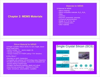
- 1. Chapter 2: MEMS Materials Materials for MEMS Materials for MEMS • Silicon (majority) • Silicon compatible materials: SixOy, SixNy • Glass • Ceramics • Polymers: photoresist, polyimide. • Compound semiconductors • Metals: Al, Ti, W, Cu, etc. • Silicon Carbides (SiC). • Other materials Silicon Material for MEMS Single Crystalline Silicon (SCS): Si, hard, fragile, cleave along crystal plane. Why Silicon? • Atomic number: 14, atomic weight: 28. • Density: ρ=2.33g/cm3, • Young’s modulus: E=170GPa (along <110> direction) • Abundant on earth: inexpensive • Compatible with existing VLSI technology (easy integration) • Excellent electrical properties: conductivity modulated with impurity doping (n-type/p-type) • Excellent mechanical properties: elastic and robust • Good thermal conductivity: 1.56W/cm·K at 300K. • Types: amorphous, polycrystalline, crystalline
- 5. Slicing and Dicing of Silicon Slicing silicon ingot into wafers Dicing silicon wafer into chips
- 6. Crystal Structure of Single-crystalline Silicon Miller Indices of Crystalline Plane/Direction It is often necessary to be able to specify certain directions and planes in crystals. Many material properties and processes vary with direction in the crystal. Directions and planes are described using three integers - Miller Indices. x, y, z are the axes (on arbitrarily positioned origin) a, b, c are lattice parameters (length of unit cell along a side) h, k, l are the Miller indices for planes and directions - expressed as planes: (hkl) and directions: [hk] Conventions for naming There are NO COMMAS between numbers Negative values are expressed with a bar over the number Example: -2 is expressed 2. Miller plane/direction symbols: plane: (hkl) (round brackets) family of planes: {hkl} (curly brackets) direction: [hkl] (square brackets) family of directions <hkl> (angle brackets)
- 7. Miller Indices of a Crystalline Direction Miller Indices of a crystalline direction: 1. Draw the vector of the direction, find the coordinates of the head, h1,k1,l1, and the tail h2,k2,l2. If vector starts from origin, then h1,k1,l1=0,0,0. 2. Subtract coordinates of tail from coordinates of head: h2- h1,k2-k1,l2-l1. 3. Multiply the result by a common factor to convert them into the smallest integer set, enclose it in square bracket, this is the Miller Indices of direction. Family of Directions All the parallel directions have the same Miller Indices. Indices in angle brackets denote a family of directions which are equivalent due to symmetry operations. For example, [100], [010], [001] or the negative of any of those directions are equivalent. They are put in angle brackets and called <100> family of directions. Miller Indices of a Plane Miller Indices of a Plane: 1. Determine the intercepts (x, y, z) of the plane along each of the three crystallographic directions. If the plane passes through the origin, select a parallel equivalent plane not passing the origin. If the plane is in parallel to an axis, the intercept is ∞. 2. Take the reciprocals of the intercepts (1/x, 1/y, 1/z). (Note:1/∞=0) 3. If fractions results, multiply each by the denominator of the smallest fraction, resulting in smallest integer set (h, k, l), which are the Miller indices of a plane. Miller Indices of a Plane Miller Indices of a Plane: Planes and their negatives are equivalent: In the cubic system, a plane and a direction with the same indices are orthogonal. E.g. [001] direction is orthogonal to (001) plane.
- 8. Linear and Planar Density Linear and planar density, Why do we care? - Properties, in general, depend on linear and planar density. Linear and Planar Density Example: Find the linear density of the [110] and the [100] direction in the FCC cell in terms of the atomic radius R. Miller Indices of a Plane Miller Indices of a Plane: Planes and their negatives are equivalent: In the cubic system, a plane and a direction with the same indices are orthogonal. E.g. [001] direction is orthogonal to (001) plane.
- 9. Silicon Wafers Identify doping type (n or p) and surface orientation of silicon wafers by judging the flats: The angle between primary and second flats can be 0°, 45°, 90° and 180°. For smaller angles (0°, 45°): (111) wafer; for larger angles (90°, 180°): (100) wafer Within each surface orientation, smaller angle (0°and 90°): p- type; larger angle (45°, 180°): n-type.
- 10. Silicon Wafer Cleaning Chemicals used for wafer cleaning • H2SO4 (sulfuric acid) • HCl (hydrocloric acid) • H2O2 (hydrogen peroxide) • NH4OH (ammonium hydroxide) • HF (hydrofluoric acid) • DI water (deionized water) Poly-silicon as MEMS Material Advantages - Compatible with VLSI technology - Good for surface micromachining Disadvantages - Residual stress during deposition - Thickness limitation: <10µm Chemical properties of Si: stable and resistant to many chemicals, but can be etched with certain etchants with good controllability.
- 11. Poly-Si MEMS micromotor ADXL150 poly-Si MEMS accelerometer Silicon Dioxide as MEMS Material Silicon oxides: SiO2, SixOy, silicate glass, etc. SiO2: very stable, electrical insulating, also used as sacrificial layers in surface micromachining, easily removed with HF. How to obtain SiO2 - Thermal oxidation Si+O2SiO2 - CVD, sputtering, spin-on. Limitations: large residual stress