Download to read offline

![2-16
S7-200 Programmable Controller System Manual
C79000-G7076-C230-02
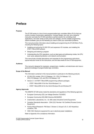
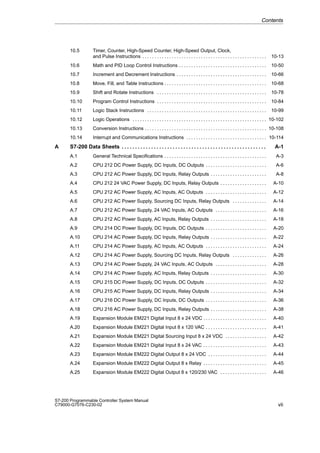
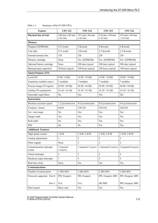
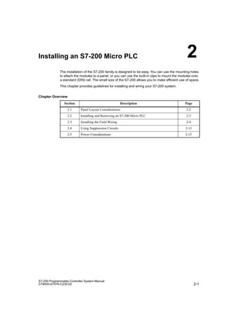
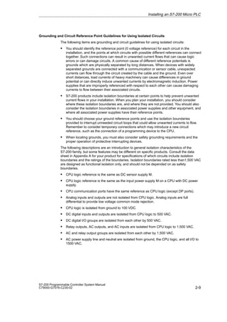
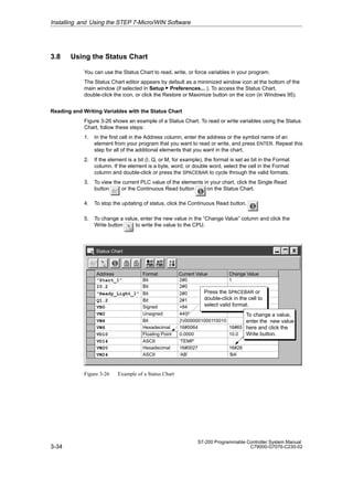
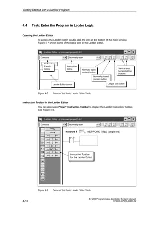
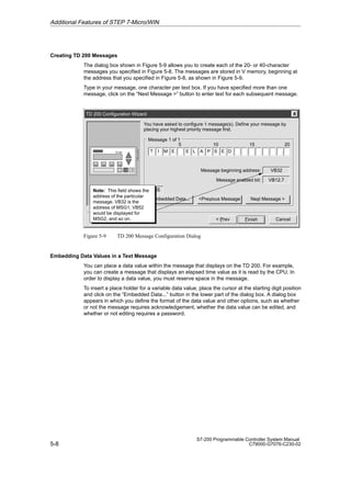
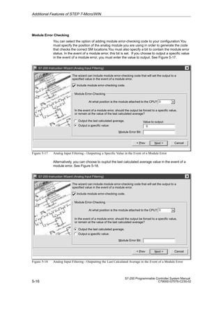
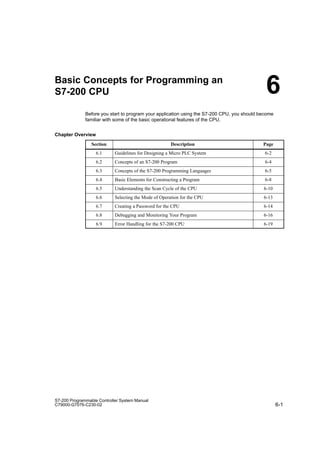
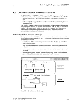
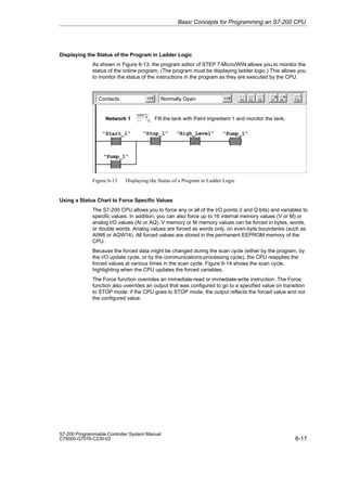
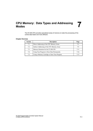
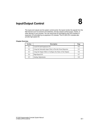
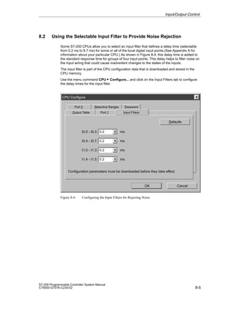
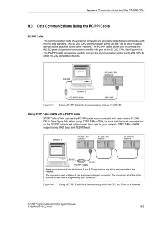
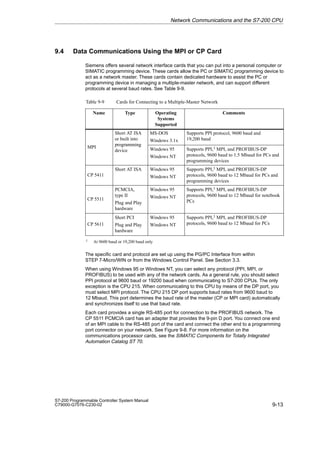
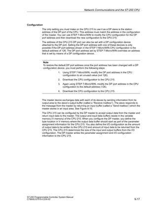
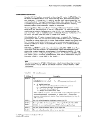
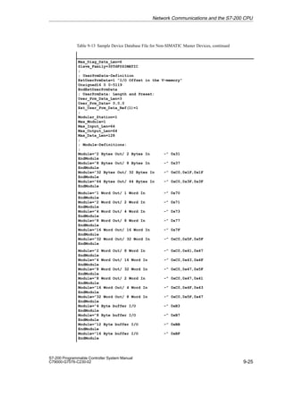
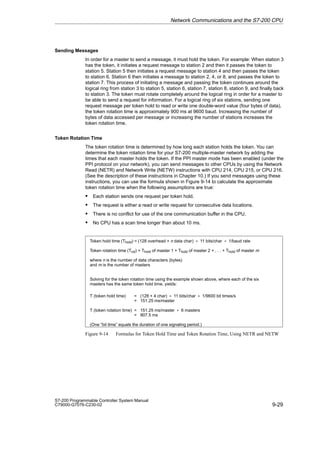
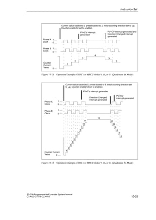
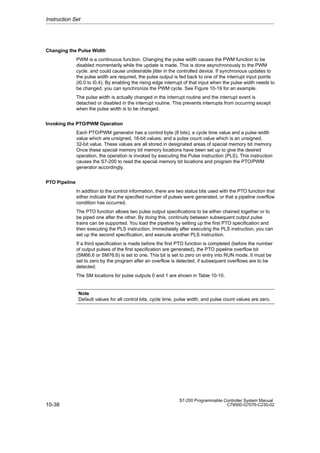
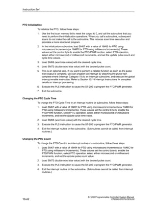
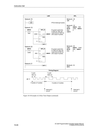
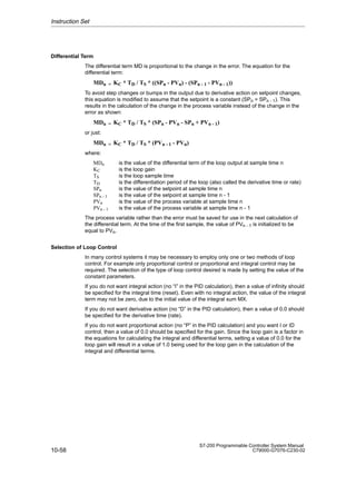
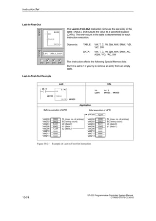
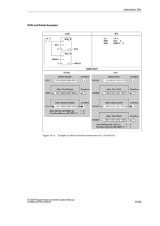
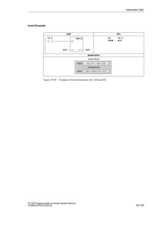
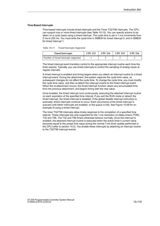
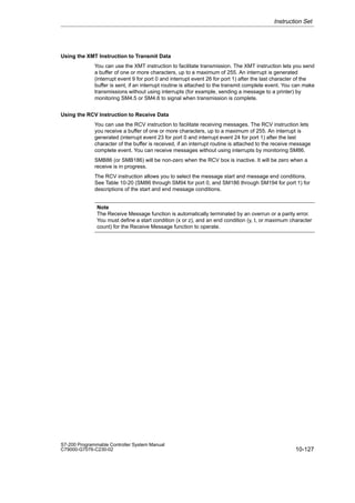
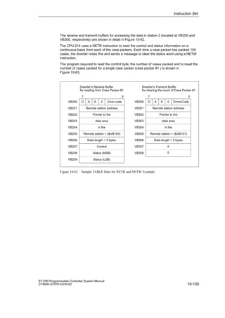
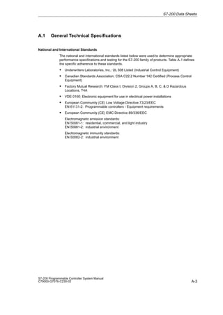
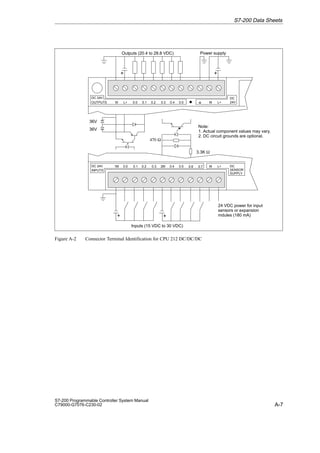
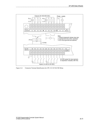
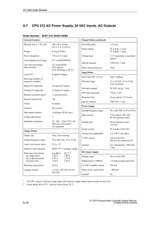
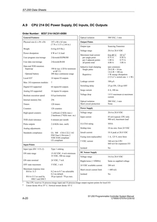
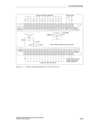
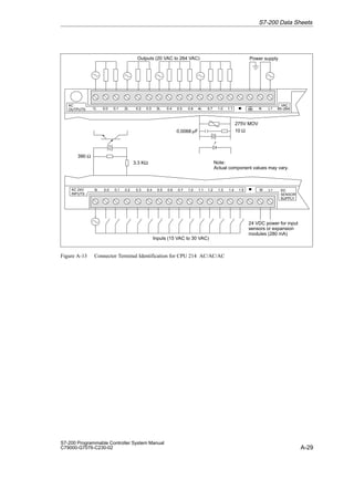
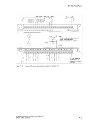
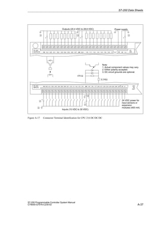
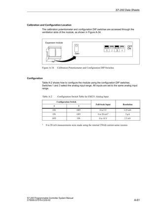
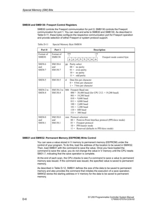
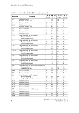
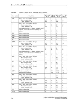
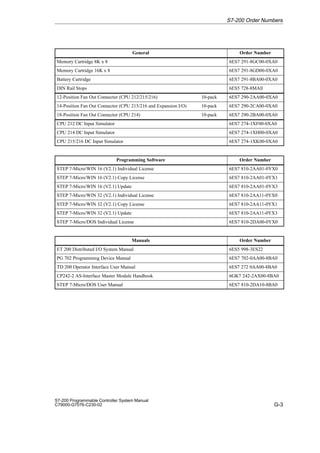
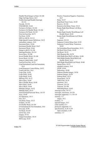
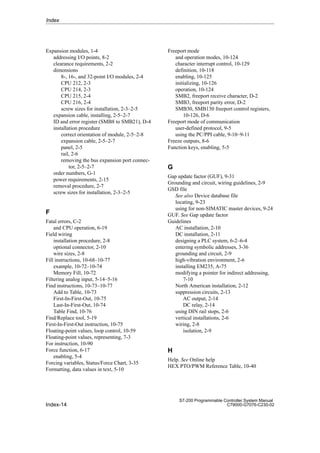
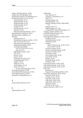
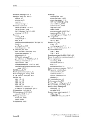
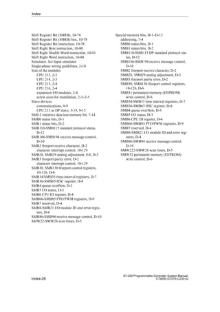
Calculating a Sample Power Requirement
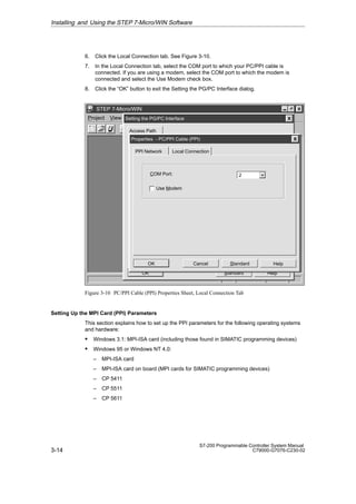
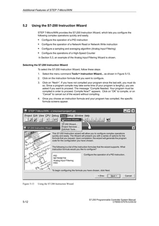
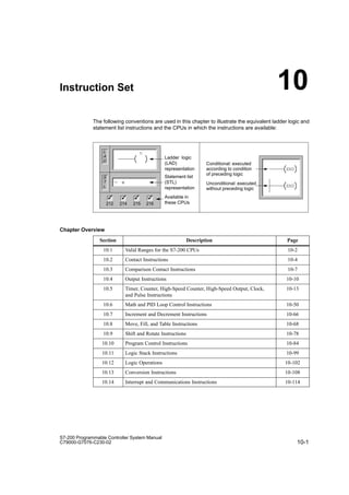
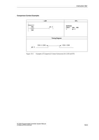
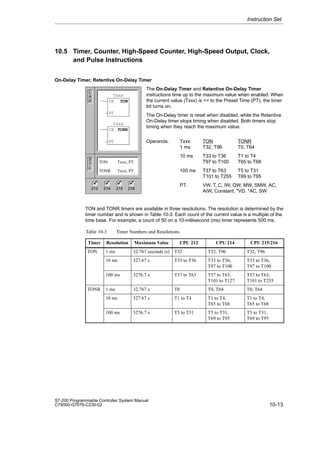
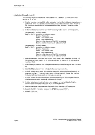
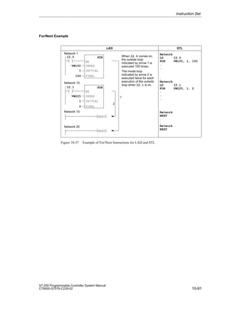
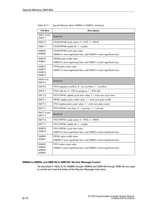
Table 2-1 shows a sample calculation of the power requirements for an S7-200 Micro PLC
that includes the following modules:
S CPU 214 DC/DC/DC
S Three EM 221 Digital Input 8 x DC 24 V expansion modules
S Two EM 222 Digital Output 8 x Relay expansion modules
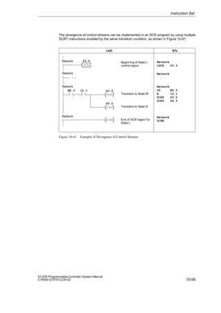
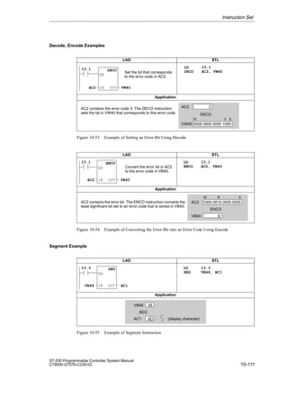
The CPU in this example provides sufficient 5 VDC current for the expansion modules;
however, it requires an additional power supply to provide the 24 VDC power requirement.
(The I/O requires 448 mA of 24 VDC power, but the CPU provides only 280 mA.) Appendix B
provides a blank power calculation table.
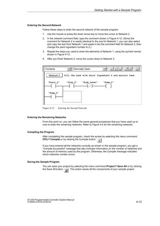
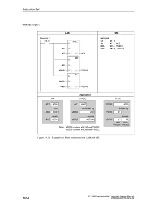
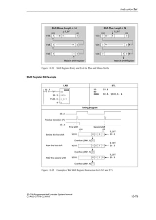
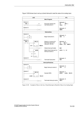
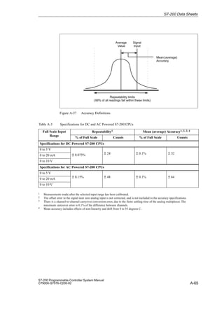
Table 2-1 Power Budget Calculations for a Sample Configuration
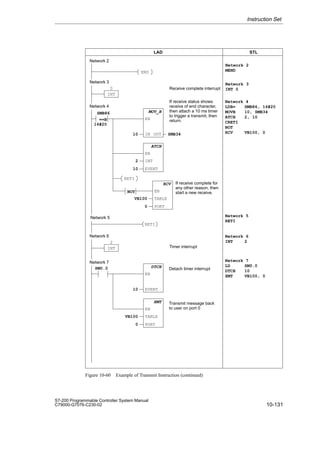
CPU Power Budget 5 VDC 24 VDC
CPU 214 DC/DC/DC 660 mA 280 mA
minus
System Requirements 5 VDC 24 VDC
CPU 214 DC/DC/DC BASE UNIT 14 input x 7 mA = 98 mA
Three EM 221 expansion modules 3 x 60 mA = 180 mA 3 x 60 mA = 180 mA
Two EM 222 expansion modules 2 x 80 mA = 160 mA 2 x 85 mA = 170 mA
Total Requirement 340 mA 448 mA
equals
Current Balance 5 VDC 24 VDC
Current Balance Total 320 mA [168 mA]
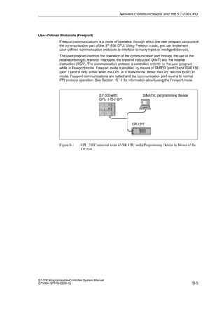
Installing an S7-200 Micro PLC](https://image.slidesharecdn.com/s7-200programmablecontrollercpu21xsystemmanual-220712183704-b560d155/85/Manual-del-sistema-del-controlador-programable-S7-200-CPU21x-30-320.jpg)


![7-3
S7-200 Programmable Controller System Manual
C79000-G7076-C230-02
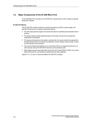
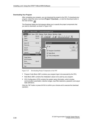
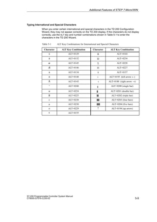
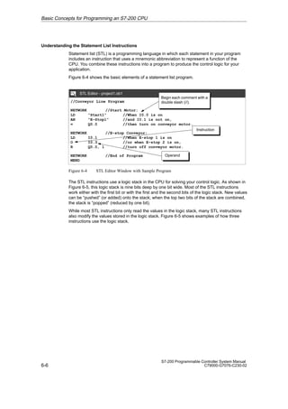
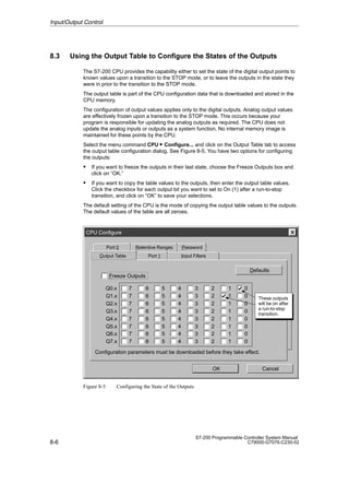
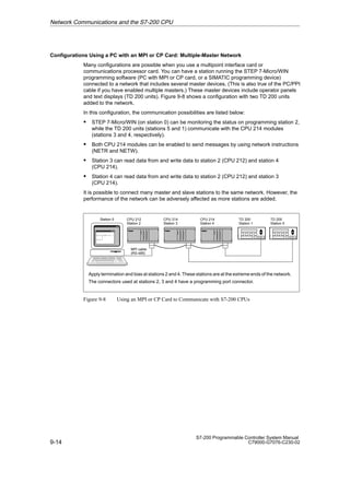
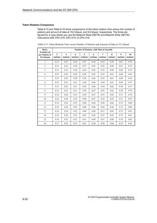
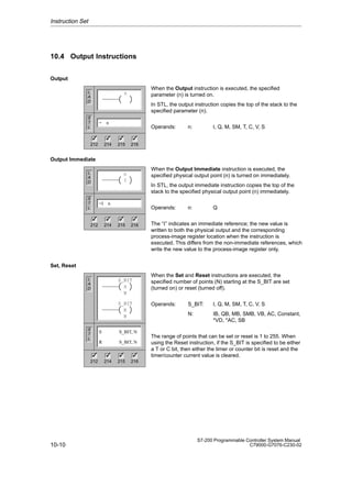
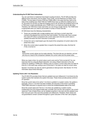
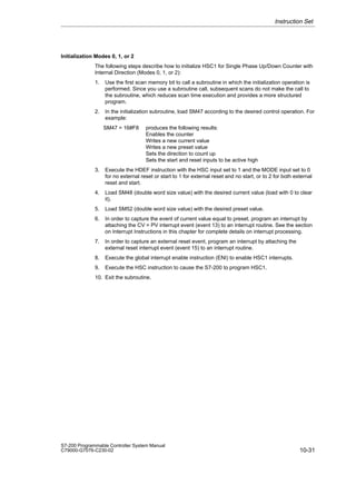
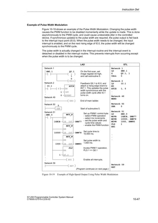
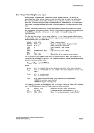
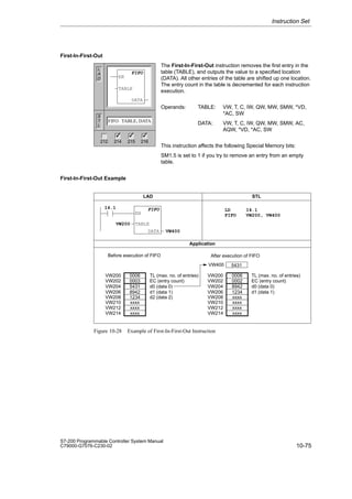
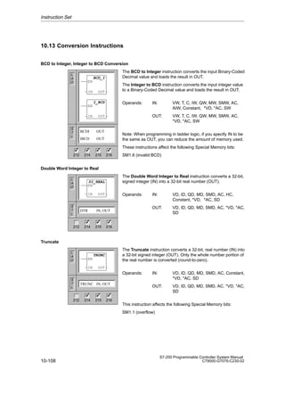
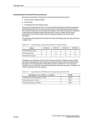
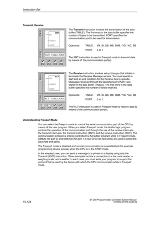
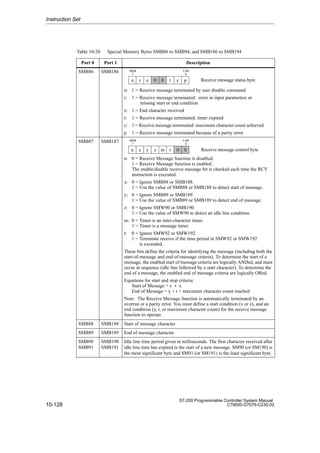
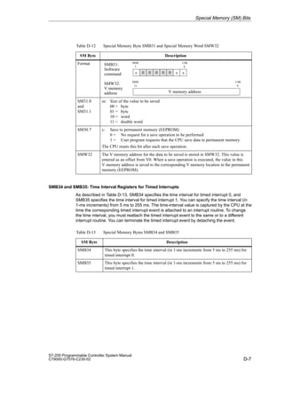
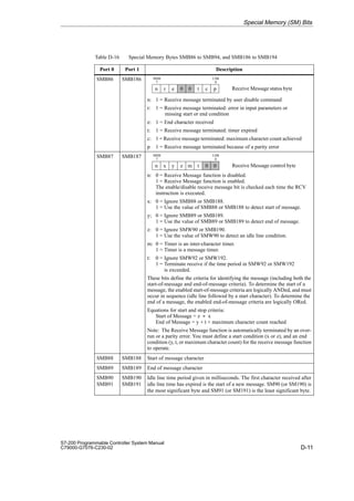
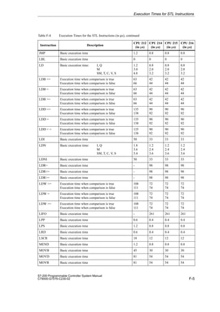
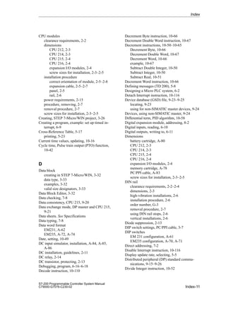
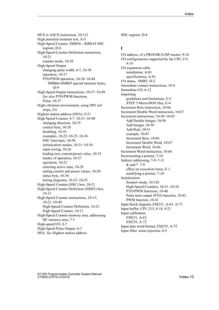
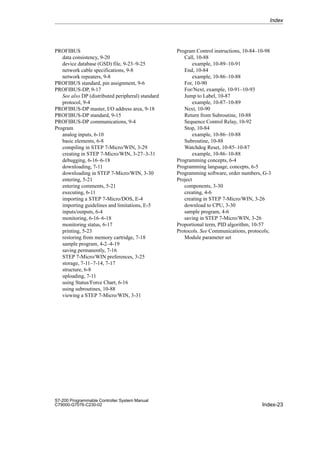
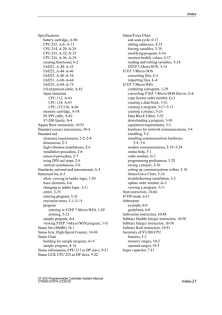
Representation of Numbers
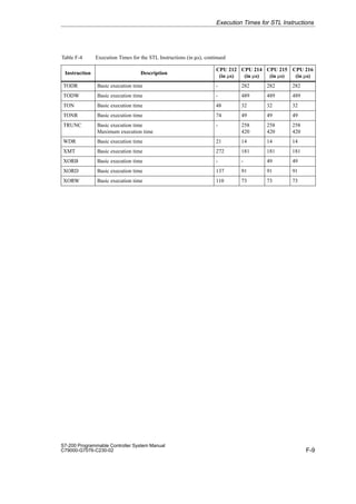
Table 7-1 shows the range of integer values that can be represented by the different sizes of
data.
Real (or floating-point) numbers are represented as 32-bit, single-precision numbers, whose
format is described in the ANSI/IEEE 754-1985 standard. Real number values are accessed
in double-word lengths.
Table 7-1 Data Size Designations and Associated Integer Ranges
Data Size
Unsigned Integer Range Signed Integer Range
Data Size
Decimal Hexadecimal Decimal Hexadecimal
B (Byte): 8-bit value 0 to 255 0 to FF -128 to 127 80 to 7F
W (Word): 16-bit value 0 to 65,535 0 to FFFF -32,768 to 32,767 8000 to 7FFF
D (Double word, Dword):
32-bit value
0 to
4,294,967,295
0 to
FFFF FFFF
-2,147,483,648 to
2,147,483,647
8000 0000 to
7FFF FFFF
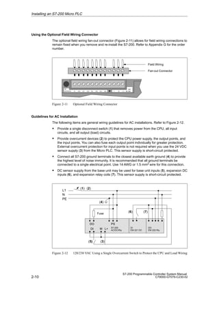
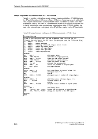
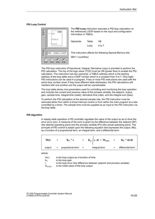
Addressing the Process-Image Input Register (I)
As described in Section 6.5, the CPU samples the physical input points at the beginning of
each scan cycle and writes these values to the process-image input register. You can access
the process-image input register in bits, bytes, words, or double words.
Format: Bit I[byte address].[bit address] I0.1
Byte, Word, Double Word I[size][starting byte address] IB4
Addressing the Process-Image Output Register (Q)
At the end of the scan cycle, the CPU copies the values stored in the process-image output
register to the physical output points. You can access the process-image output register in
bits, bytes, words, or double words.
Format: Bit Q[byte address].[bit address] Q1.1
Byte, Word, Double Word Q[size][starting byte address] QB5
Addressing the Variable (V) Memory Area
You can use V memory to store intermediate results of operations being performed by the
control logic in your program. You can also use V memory to store other data pertaining to
your process or task. You can access the V memory area in bits, bytes, words, or double
words.
Format: Bit V[byte address].[bit address] V10.2
Byte, Word, Double Word V[size][starting byte address] VW100
Addressing the Bit Memory (M) Area
You can use the internal memory bits (M memory) as control relays to store the intermediate
status of an operation or other control information. While the name “bit memory area” implies
that this information is stored in bit-length units, you can access the bit memory area not only
in bits, but also in bytes, words, or double words.
Format: Bit M[byte address].[bit address] M26.7
Byte, Word, Double Word M[size][starting byte address] MD20
CPU Memory: Data Types and Addressing Modes](https://image.slidesharecdn.com/s7-200programmablecontrollercpu21xsystemmanual-220712183704-b560d155/85/Manual-del-sistema-del-controlador-programable-S7-200-CPU21x-133-320.jpg)
![7-4
S7-200 Programmable Controller System Manual
C79000-G7076-C230-02
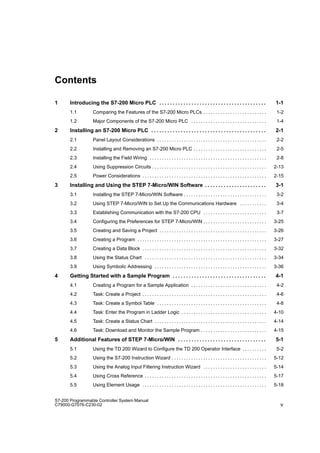
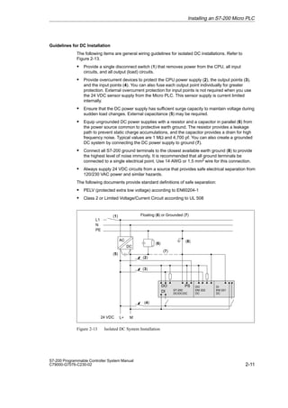
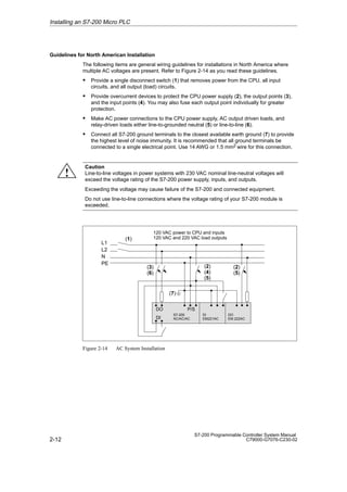
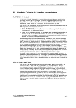
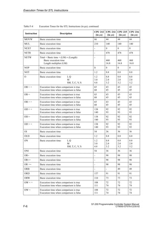
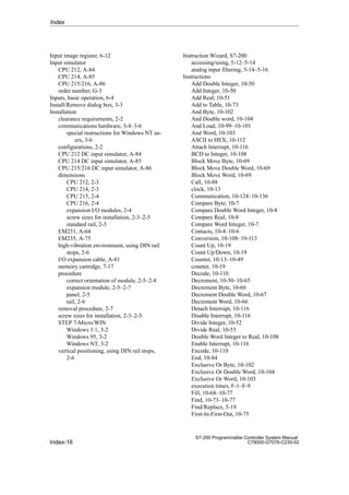
Addressing the Sequence Control Relay (S) Memory Area
Sequence Control Relay bits (S) are used to organize machine operations or steps into
equivalent program segments. SCRs allow logical segmentation of the control program. You
can access the S bits as bits, bytes, words, or double words.
Format: Bit S[byte address].[bit address] S3.1
Byte, Word, Double Word S[size][starting byte address] SB4
Addressing the Special Memory (SM) Bits
The SM bits provide a means for communicating information between the CPU and your
program. You can use these bits to select and control some of the special functions of the
S7-200 CPU, such as:
S A bit that turns on for the first scan
S Bits that toggle at fixed rates
S Bits that show the status of math or operational instructions
For more information about the SM bits, see Appendix D. While the SM area is based on
bits, you can access the data in this area as bits, bytes, words, or double words.
Format: Bit SM[byte address].[bit address] SM0.1
Byte, Word, Double Word SM[size][starting byte address] SMB86
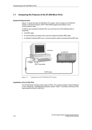
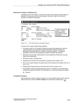
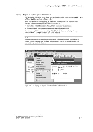
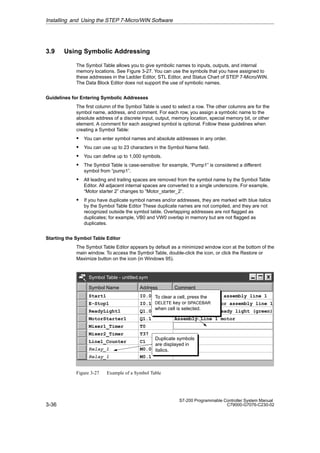
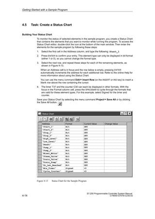
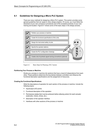
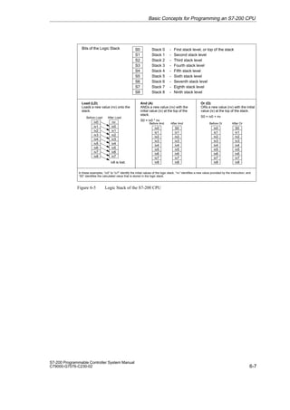
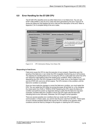
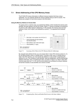
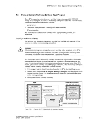
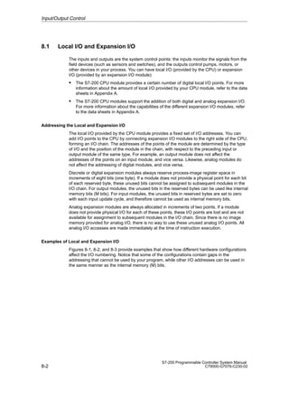
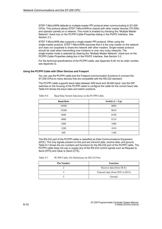
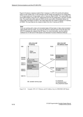
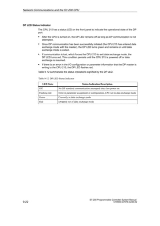
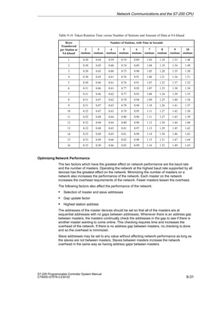
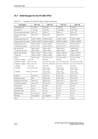
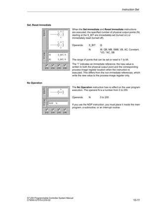
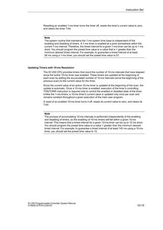
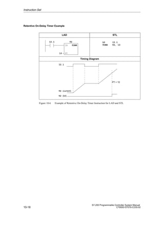
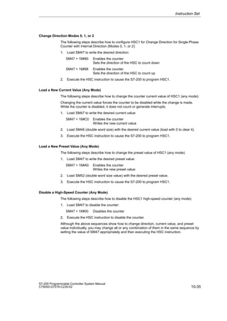
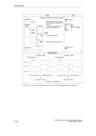
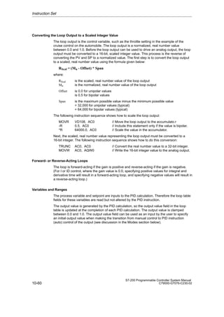
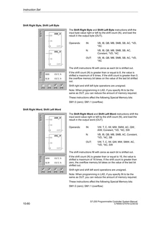
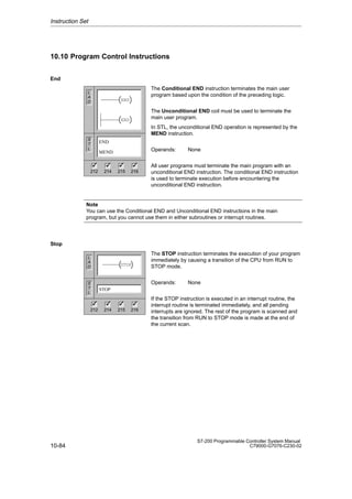
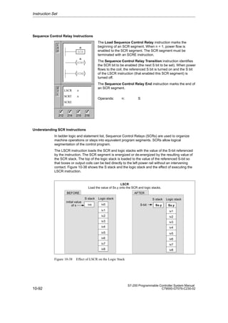
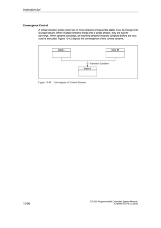
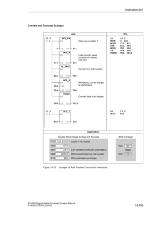
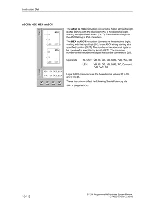
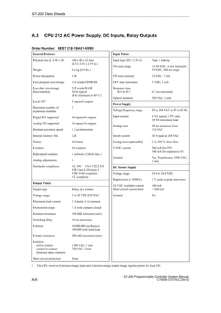
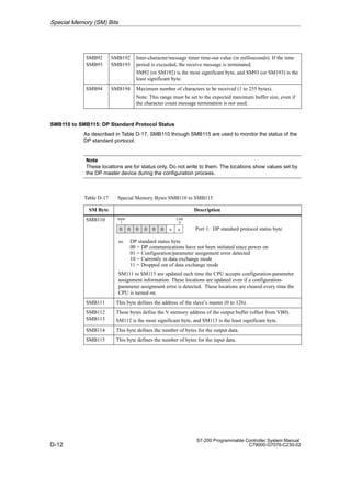
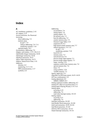
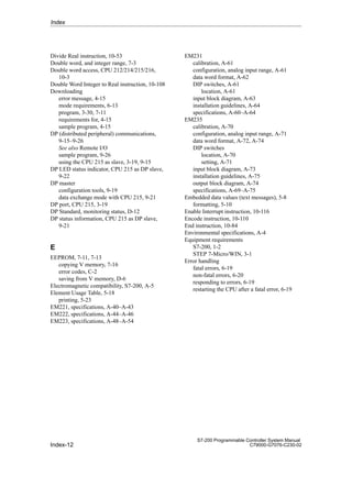
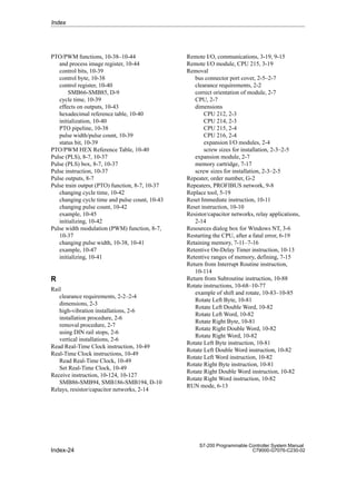
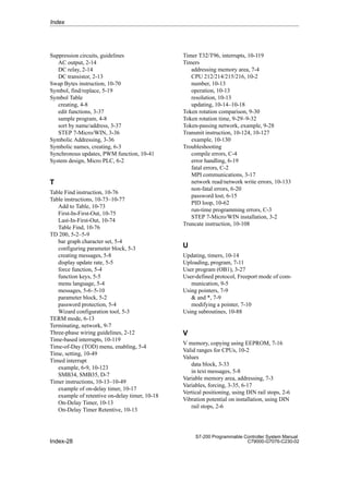
Addressing the Timer (T) Memory Area
In the S7-200 CPU, timers are devices that count increments of time. The S7-200 timers
have resolutions (time-base increments) of 1 ms, 10 ms, or 100 ms. There are two variables
that are associated with a timer:
S Current value: this 16-bit signed integer stores the amount of time counted by the timer.
S Timer bit: this bit turns on (is set to 1) when the current value of the timer is greater than
or equal to the preset value. (The preset value is entered as part of the timer instruction.)
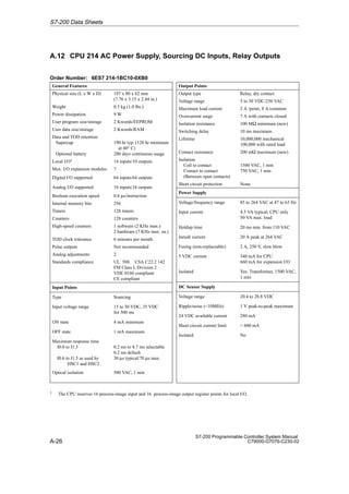
You access both of these variables by using the timer address (T + timer number). Access to
either the timer bit or the current value is dependent on the instruction used: instructions with
bit operands access the timer bit, while instructions with word operands access the current
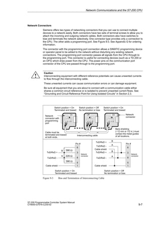
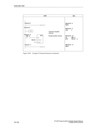
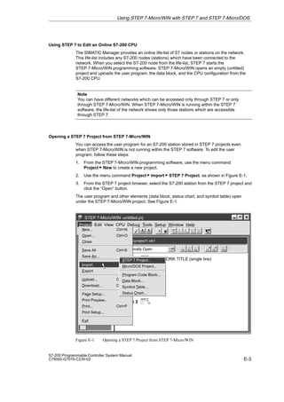
value. As shown in Figure 7-3, the Normally Open Contact instruction accesses the timer bit,
while the Move Word (MOV_W) instruction accesses the current value of the timer. For more
information about the S7-200 instruction set, refer to Chapter 10.
Format: T[timer number] T24
CPU Memory: Data Types and Addressing Modes](https://image.slidesharecdn.com/s7-200programmablecontrollercpu21xsystemmanual-220712183704-b560d155/85/Manual-del-sistema-del-controlador-programable-S7-200-CPU21x-134-320.jpg)
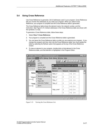
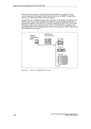
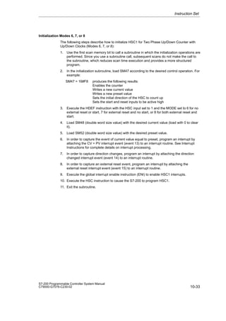
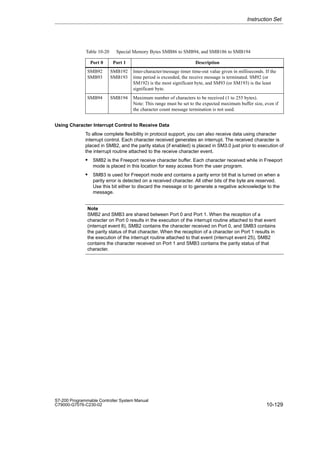
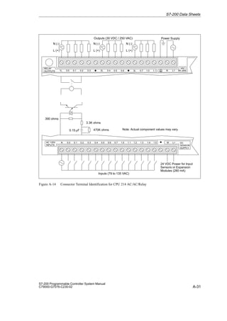
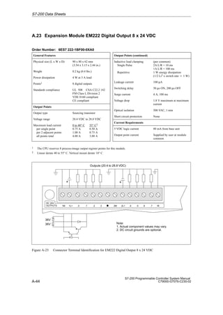
![7-5
S7-200 Programmable Controller System Manual
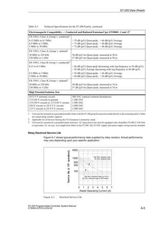
C79000-G7076-C230-02
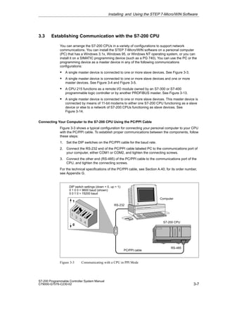
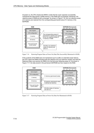
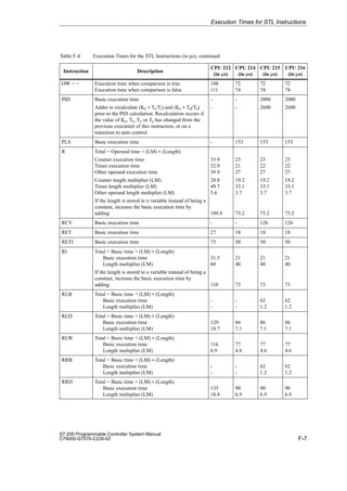
Current Value
T0
T3
T0
Timer Bits (Read/Write)
T1
T2
T1
T2
T3
I2.1 MOV_W
EN
OUT VW200
IN
T2
T3
Area identifier (timer)
Timer number (bit address)
Timer number
(current value address)
Area identifier (timer)
15
MSB LSB
0
Current Value of the Timer
(Read/Write)
T0
T3
T0
Timer Bits
T1
T2
T1
T2
T3
Figure 7-3 Accessing the Timer Data
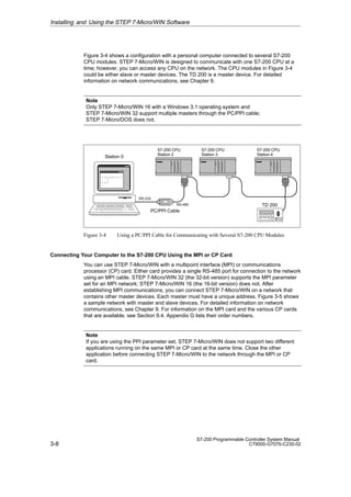
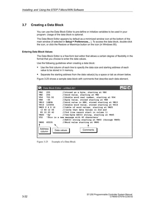
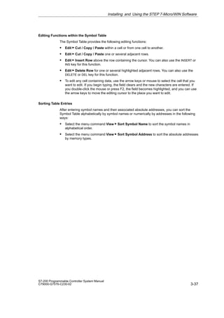
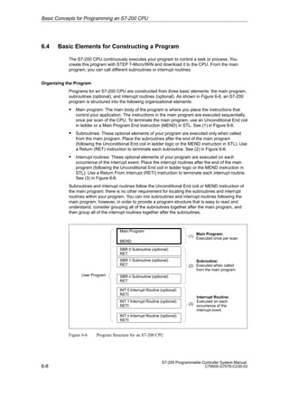
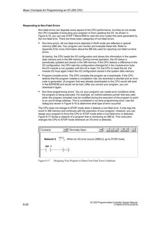
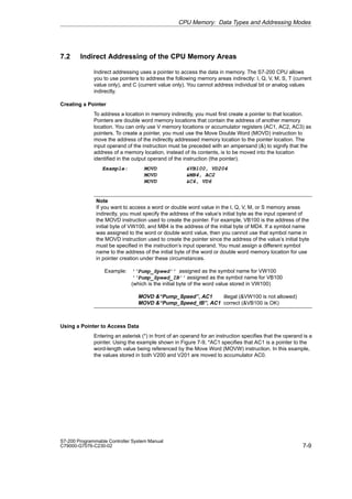
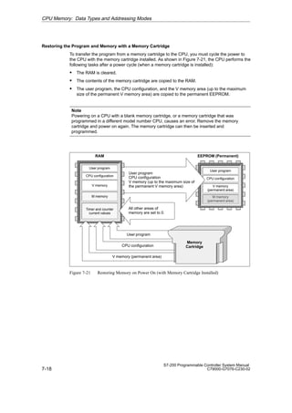
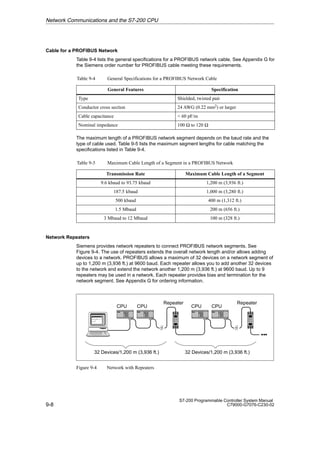
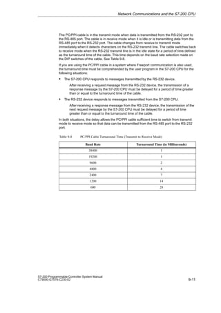
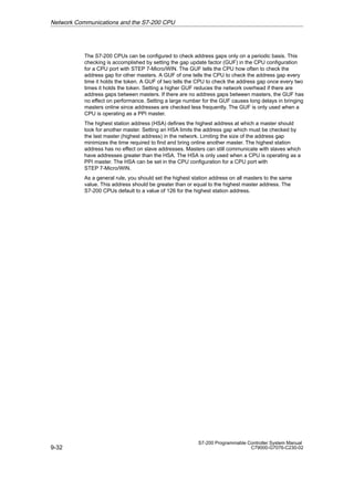
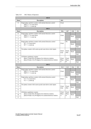
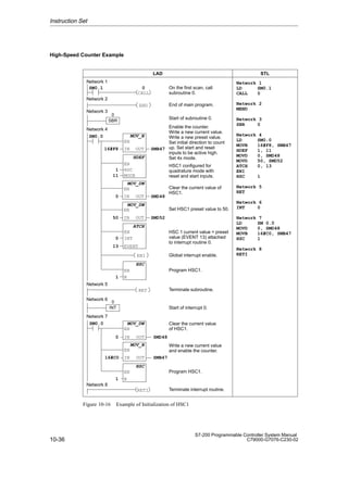
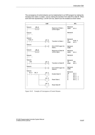
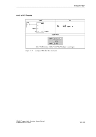
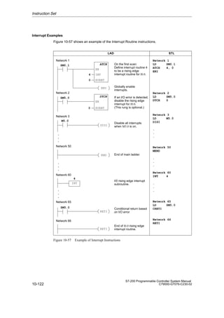
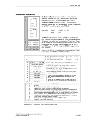
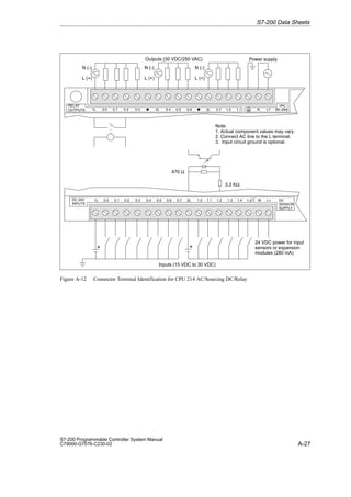
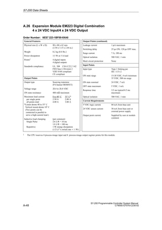
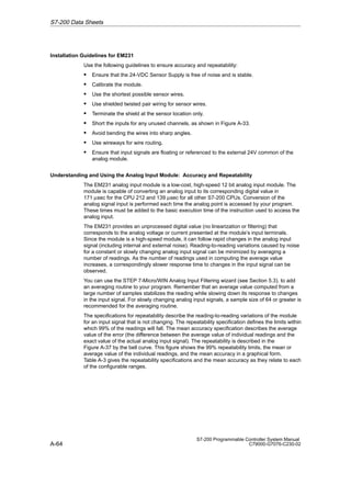
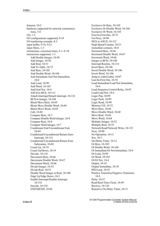
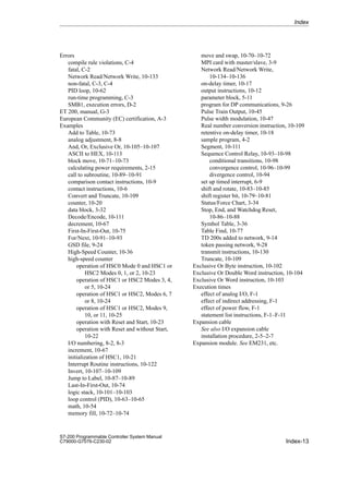
Addressing the Counter (C) Memory Area
In the S7-200 CPU, counters are devices that count each low-to-high transition event on the
counter input(s). The CPU provides two types of counters: one type counts up only, and the
other counts both up and down. There are two variables that are associated with a counter:
S Current value: this 16-bit signed integer stores the accumulated count.
S Counter bit: this bit turns on (is set to 1) when the current value of the counter is greater
than or equal to the preset value. (The preset value is entered as part of the counter
instruction.)
You access both of these variables by using the counter address (C + counter number).
Access to either the counter bit or the current value is dependent on the instruction used:
instructions with bit operands access the counter bit, while instructions with word operands
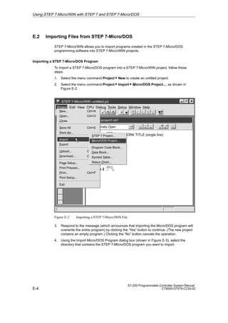
access the current value. As shown in Figure 7-4, the Normally Open Contact instruction
accesses the counter bit, while the Move Word (MOV_W) instruction accesses the current
value of the counter. For more information about the S7-200 instruction set, refer to
Chapter 10.
Format: C[counter number] C20
Current Value
C0
C3
C0
Counter Bits
(Read/Write)
C1
C2
C1
C2
C3
I2.1 MOV_W
EN
OUT VW200
IN
C2
C3
Counter number
(current value address)
Area identifier (counter)
15
MSB LSB
0
Current Value
(Read/Write)
C0
C3
C0
Counter
Bits
C1
C2
C1
C2
C3
Counter number (bit address)
Area identifier (counter)
Figure 7-4 Accessing the Counter Data
CPU Memory: Data Types and Addressing Modes](https://image.slidesharecdn.com/s7-200programmablecontrollercpu21xsystemmanual-220712183704-b560d155/85/Manual-del-sistema-del-controlador-programable-S7-200-CPU21x-135-320.jpg)
![7-6
S7-200 Programmable Controller System Manual
C79000-G7076-C230-02
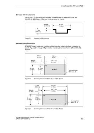
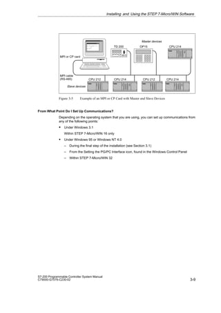
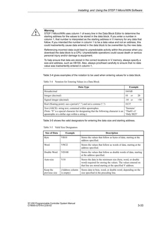
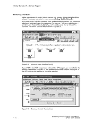
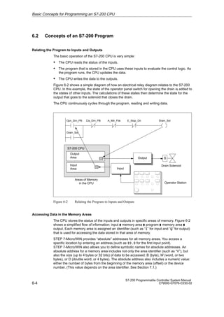
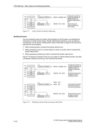
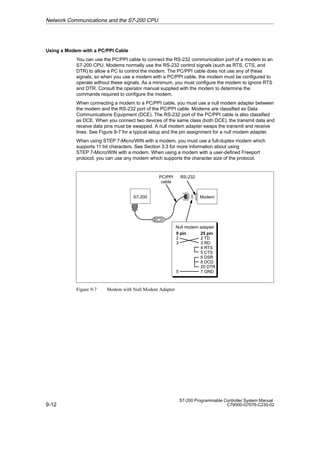
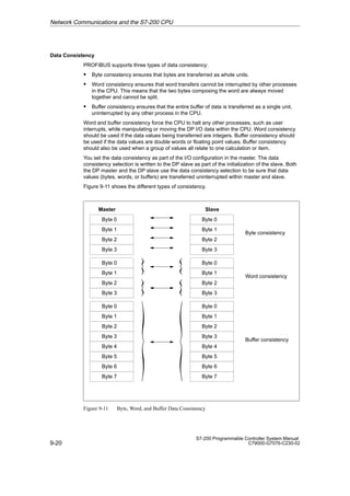
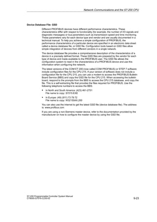
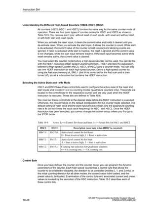
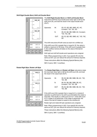
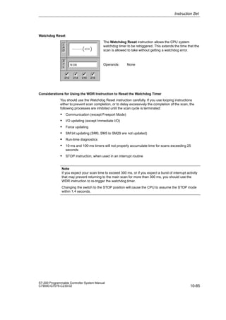
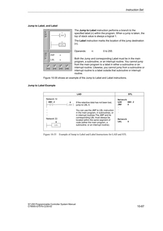
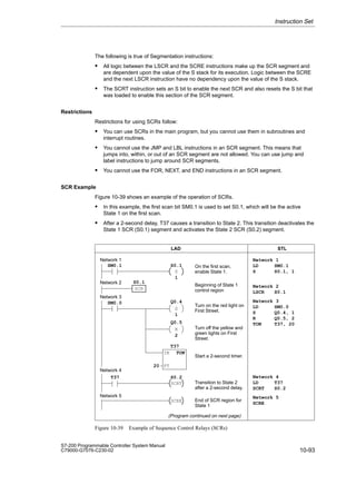
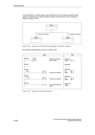
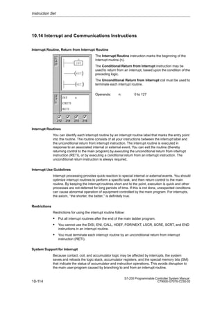
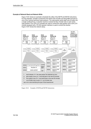
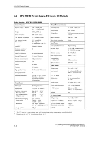
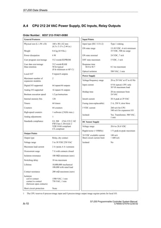
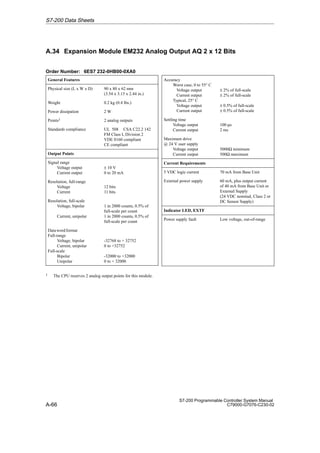
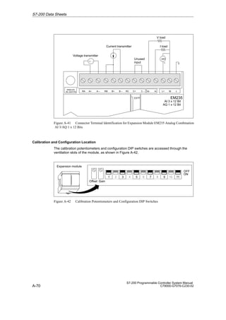
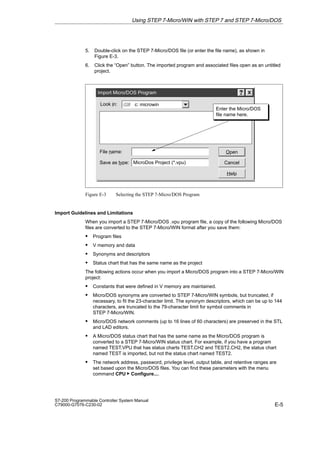
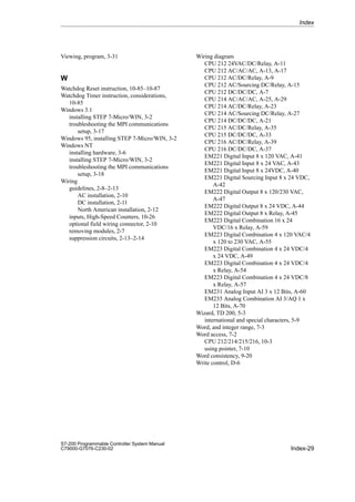
Addressing the Analog Inputs (AI)
The S7-200 converts a real-world, analog value (such as temperature or voltage) into a
word-length (16-bit) digital value. You access these values by the area identifier (AI), size of
the data (W), and the starting byte address. Since analog inputs are words and always start
on even-number bytes (such as 0, 2, or 4), you access them with even-number byte
addresses (such as AIW0, AIW2, or AIW4), as shown in Figure 7-5. Analog input values are
read-only values.
Format: AIW[starting byte address] AIW4
AI W 8
Area identifier (analog input)
Access to a word-size value
Byte address
AIW8 byte 8 byte 9
15 8
MSB
7 0
LSB
Least significant byte
Most significant byte
Figure 7-5 Accessing an Analog Input
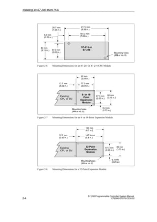
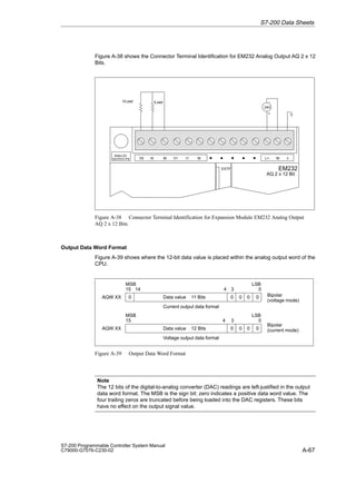
Addressing the Analog Outputs (AQ)
The S7-200 converts a word-length (16-bit) digital value into a current or voltage,
proportional to the digital value (such as for a current or voltage). You write these values by
the area identifier (AQ), size of the data (W), and the starting byte address. Since analog
outputs are words and always start on even-number bytes (such as 0, 2, or 4), you write
them with even-number byte addresses (such as AQW0, AQW2, or AQW4), as shown in
Figure 7-6. Your program cannot read the values of the analog outputs.
Format: AQW[starting byte address] AQW4
AQ W 10
Area identifier (analog output)
Access to a word-size value
Byte address
AQW10 byte 10 byte 11
15 8
MSB
7 0
LSB
Least significant byte
Most significant byte
Figure 7-6 Accessing an Analog Output
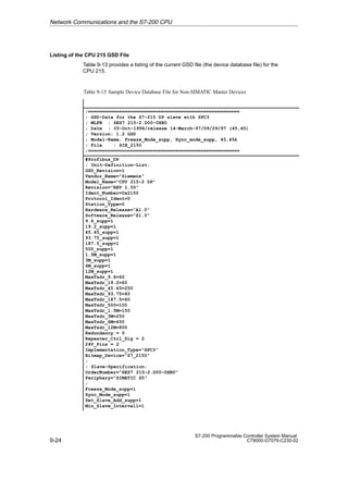
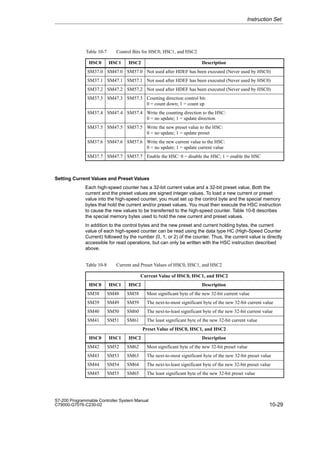
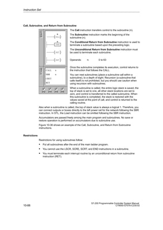
Addressing the Accumulators (AC)
Accumulators are read/write devices that can be used like memory. For example, you can
use accumulators to pass parameters to and from subroutines and to store intermediate
values used in a calculation. The CPU provides four 32-bit accumulators (AC0, AC1, AC2,
and AC3). You can access the data in the accumulators as bytes, words, or double words.
As shown in Figure 7-7, to access the accumulator as bytes or words you use the least
significant 8 or 16 bits of the value that is stored in the accumulator. To access the
accumulator as a double word, you use all 32 bits. The size of the data being accessed is
determined by the instruction that is used to access the accumulator.
Format: AC[accumulator number] AC0
Note
See Section 10.14 for information about using the accumulators with interrupt routines.
CPU Memory: Data Types and Addressing Modes](https://image.slidesharecdn.com/s7-200programmablecontrollercpu21xsystemmanual-220712183704-b560d155/85/Manual-del-sistema-del-controlador-programable-S7-200-CPU21x-136-320.jpg)
![7-7
S7-200 Programmable Controller System Manual
C79000-G7076-C230-02
MOV_B
EN
OUT VB200
IN
AC2
MSB
7 0
LSB
DEC_W
EN
OUT VW100
IN
AC1
15 0
LSB
INV_D
EN
OUT VD250
IN
AC3
31
MSB
0
LSB
AC2 (accessed as a byte)
AC1 (accessed as a word)
AC3 (accessed as a double word)
MSB
Accumulator number
Area identifier (Accumulator)
Accumulator number
Area identifier (Accumulator)
Accumulator number
Area identifier (Accumulator)
7
8
7
8
15
16
23
24
Least significant
Most significant
Least significant
Most significant
Byte 0
Byte 1
Byte 0
Byte 1
Byte 2
Byte 3
Figure 7-7 Addressing the Accumulators
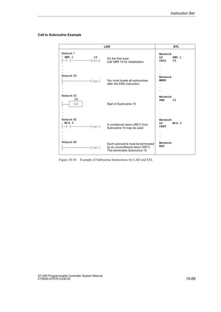
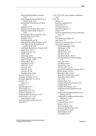
Addressing the High-Speed Counters (HC)
High-speed counters are designed to count events faster than the CPU can scan the events.
High-speed counters have a signed, 32-bit integer counting value (or current value). To
access the count value for the high-speed counter, you specify the address of the
high-speed counter, using the memory type (HC) and the counter number (such as HC0).
The current value of the high-speed counter is a read-only value and, as shown in
Figure 7-8, can be addressed only as a double word (32 bits).
Format: HC[high-speed counter number] HC1
HC 2
HC2
31
MSB
0
LSB
High-speed counter number
Area identifier (high-speed counter)
Least significant
Most significant
Byte 0
Byte 1
Byte 2
Byte 3
Figure 7-8 Accessing the High-Speed Counter Current Values
CPU Memory: Data Types and Addressing Modes](https://image.slidesharecdn.com/s7-200programmablecontrollercpu21xsystemmanual-220712183704-b560d155/85/Manual-del-sistema-del-controlador-programable-S7-200-CPU21x-137-320.jpg)
![7-8
S7-200 Programmable Controller System Manual
C79000-G7076-C230-02
Using Constant Values
You can use a constant value in many of the S7-200 instructions. Constants can be bytes,
words, or double words. The CPU stores all constants as binary numbers, which can then be
represented in decimal, hexadecimal, or ASCII formats.
Decimal Format: [decimal value]
Hexadecimal Format: 16#[hexadecimal value]
ASCII Format: ’[ASCII text]’
The S7-200 CPU does not support “data typing” or data checking (such as specifying that
the constant is stored as an integer, a signed integer, or a double integer). For example, an
Add instruction can use the value in VW100 as a signed integer value, while an Exclusive Or
instruction can use the same value in VW100 as an unsigned binary value.
The following examples show constants for decimal, hexadecimal, and ASCII format:
S Decimal constant: 20047
S Hexadecimal constant: 16#4E4F
S ASCII constant: ·Text goes between single quotes.·
CPU Memory: Data Types and Addressing Modes](https://image.slidesharecdn.com/s7-200programmablecontrollercpu21xsystemmanual-220712183704-b560d155/85/Manual-del-sistema-del-controlador-programable-S7-200-CPU21x-138-320.jpg)
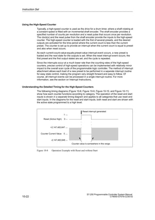
![10-26
S7-200 Programmable Controller System Manual
C79000-G7076-C230-02
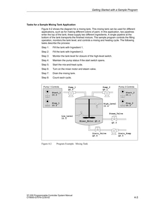
Connecting the Input Wiring for the High-Speed Counters
Table 10-4 shows the inputs used for the clock, direction control, reset, and start functions
associated with the high-speed counters. These input functions are described in Table 10-5.
Table 10-4 Dedicated Inputs for High-Speed Counters
High-Speed Counter Inputs Used
HSC0 I0.0
HSC1 I0.6, I0.7, I1.0, I1.1
HSC2 I1.2, I1.3, I1.4, I1.5
Addressing the High-Speed Counters (HC)
To access the count value for the high-speed counter, you specify the address of the
high-speed counter, using the memory type (HC) and the counter number (such as HC0).
The current value of the high-speed counter is a read-only value and can be addressed only
as a double word (32 bits), as shown in Figure 10-15.
Format: HC[high-speed counter number] HC1
HC 2
HC2
31
MSB
0
LSB
High-speed counter number
Area identifier (high-speed counter)
Least significant
Most significant
Byte 0
Byte 1
Byte 2
Byte 3
Figure 10-15 Accessing the High-Speed Counter Current Values
Instruction Set](https://image.slidesharecdn.com/s7-200programmablecontrollercpu21xsystemmanual-220712183704-b560d155/85/Manual-del-sistema-del-controlador-programable-S7-200-CPU21x-214-320.jpg)
![10-78
S7-200 Programmable Controller System Manual
C79000-G7076-C230-02
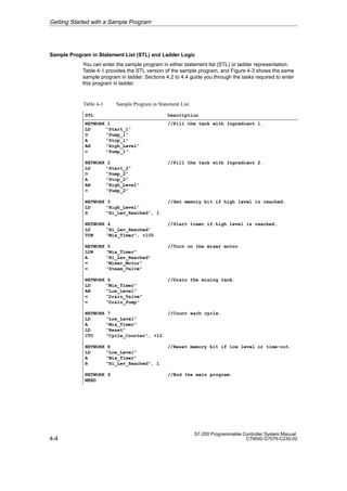
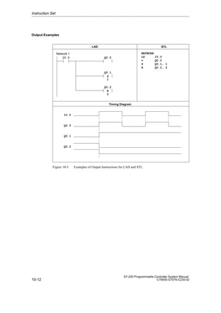
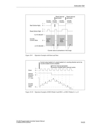
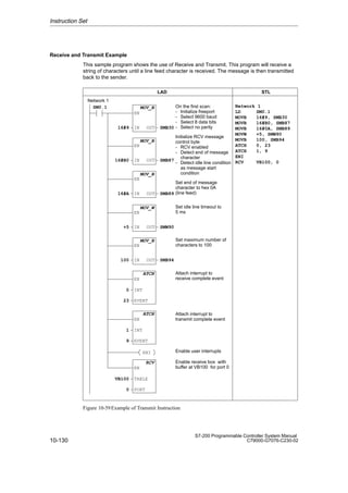
10.9 Shift and Rotate Instructions
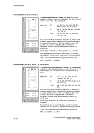
Shift Register Bit
The Shift Register Bit instruction shifts the value of DATA into
the Shift Register. S_BIT specifies the least significant bit of the
Shift Register. N specifies the length of the Shift Register and
the direction of the shift (Shift Plus = N, Shift Minus = -N).
Operands: DATA, S_BIT: I, Q, M, SM, T, C, V, S
N: VB, IB, QB, MB, SMB, AC,
Constant, *VD, *AC, SB
Understanding the Shift Register Bit Instruction
The Shift Register Bit instruction provides an easy method for the sequencing and controlling
of product flow or data. Use the Shift Register Bit instruction to shift the entire register one bit,
once per scan. The Shift Register Bit instruction is defined by both the least significant bit
(S_BIT) and the number of bits specified by the length (N). Figure 10-32 shows an example
of the Shift Register Bit instruction.
The address of the most significant bit of the Shift Register (MSB.b) can be computed by the
following equation:
MSB.b = [(Byte of S_BIT) + ([N] - 1 + (bit of S_BIT)) / 8] . [remainder of the division by 8]
You must subtract 1 bit because S_BIT is one of the bits of the Shift Register.
For example, if S_BIT is V33.4, and N is 14, then the MSB.b is V35.1, or:
MSB.b = V33 + ([14] - 1 +4)/8
= V33 + 17/8
= V33 + 2 with a remainder of 1
= V35.1
On a Shift Minus, indicated by a negative value of length (N), the input data shifts into the
most significant bit of the Shift Register, and shifts out of the least significant bit (S_BIT).
On a Shift Plus, indicated by a positive value of length (N), the input data (DATA) shifts into
the least significant bit of the Shift Register, specified by the S_BIT, and out of the most
significant bit of the Shift Register.
The data shifted out is then placed in the overflow memory bit (SM1.1). The maximum length
of the shift register is 64 bits, positive or negative. Figure 10-31 shows bit shifting for negative
and positive values of N.
Instruction Set
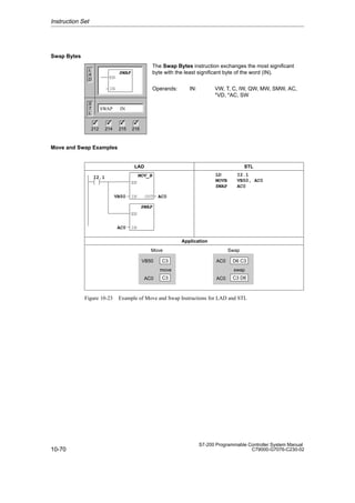
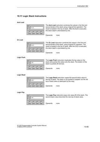
L
A
D
S
T
L
SHRB DATA, S_BIT, N
212 214 215 216
✓ ✓ ✓
✓
SHRB
EN
S_BIT
N
DATA](https://image.slidesharecdn.com/s7-200programmablecontrollercpu21xsystemmanual-220712183704-b560d155/85/Manual-del-sistema-del-controlador-programable-S7-200-CPU21x-266-320.jpg)


This document provides an overview and introduction to programming and using the S7-200 Micro PLC system. It describes installing the hardware, programming software, and entering sample programs. Key topics covered include comparing features of different CPU models, installing the CPU and I/O modules, setting up the STEP 7-Micro/WIN software, and programming basics such as ladder logic, data types, and instructions. The document also provides additional reference material on communications, the instruction set, and troubleshooting.