This document discusses memory mapped I/O, the MSP430 architecture including memory, CPU, and peripherals. It describes the MSP430 Launchpad development board and how to control the onboard LEDs and button using the general purpose input/output ports and interrupts. It provides examples of state machine programming and using timer interrupts to implement functions like recording the time of button presses.
Switch Control and Time Delay
1. LEDs and switches
2. Keypad and LEDs
3. Keypad and 8-segment LED C language and Assembly Code for Freescale MC9S08AW60
Cataloge ge 3.control and_automation_dienhathe.com-4_20_vat300_e_c6-6-4_1_rev_bDien Ha The
Khoa Học - Kỹ Thuật & Giải Trí: http://phongvan.org
Tài Liệu Khoa Học Kỹ Thuật: http://tailieukythuat.info
Thiết bị Điện Công Nghiệp - Điện Hạ Thế: http://dienhathe.vn
This note is more helpful to S7 CSE students Under kerala University. It Contains the architecture and memory organization PIC 16f873 Microcontrollers.
BASIC INFORMATION OF ARCHITECTURE OF MICRO-CONTROLLER 8051 AS PER GTU SYLLABUS. Please Comment if u Like.. n Give u r feedback..
For More Information Go to
http://www.noesiseducation.blogspot.com
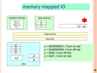
1. memory mapped IO
Data BUS
data memory
CPU
program memory
pc
sp
ALU
LD r1, a
LD r2, b
ADD r1,r2
ST c
r0
r1
r2
r3
a
b
c
Address BUS
b0
b1
y = 0b00000001; // turn on red
y = 0b00000000; // turn off red
y = 0x00; // turn off red
y = 0x01; // turn on red
2. LAUNCHPAD DEVELOPMENT BOARD
Embedded Emulation
6-pin eZ430
Connector
Part and Socket
Crystal Pads
Power Connector
Reset Button
LEDs and Jumpers
P1.0 & P1.6
P1.3 Button
Chip
Pinouts
USB Emulator
Connection
• 16kB Flash
• 512B RAM
• 2 Timer_A3’s
• 8 Ch. Comp_A+
• 8 Ch. ADC10
• USCI
10
3. Copyright 2009 Texas Instruments
All Rights Reserved
www.msp430.ubi.pt
3
MSP 430 ARCHITECTURE
Architecture Overview
Memory
CPU
Peripherals
4. Copyright 2009 Texas Instruments
All Rights Reserved
www.msp430.ubi.pt
4
MSP430 ARCHITECTURE
5. Copyright
2009
Texas
Instruments
All
Rights
Reserved
www.msp430.ubi.pt
5
MEMORY
Memory Data Size
Byte, Word, Long Word
Byte = 8 bits
Word = 16 bits
Long Word = 32 bits
Memory Address
Address size = 20 bits
Total addresses = 220 = 1 M
Each address holds 8 bits
A byte requires one address
A word requires two address
A long word requires four
addresses
RAM Memory
Random Access Memory,
Read/Write Memory,
Holds data as long as power is
applied
Used for changing data
Flash Memory
Read/ Write memory
Holds information even after
the power is turned off
Used to store programs and
fixed data
7. MSP430 CPU
R2
R3
R4
R5
R7
R8
R10
R9
R11
R12
R13
R6
R14
R15
R0 / PC (Program Counter)
R1 / SP (Stack Pointer)
R2 / CG1
R3 / CG2
R4
R5
R7
R8
R10
R9
R11
R12
R13
R6
R14
R15
20-bit
Address
16-bit
Data
Memory Map …
6
16 Registers R0 – R15
Each register holds 16
bits of information
Special Registers:
PC, SP
Registers are used for
temporary data
PC provides program
memory addresses
SP provides stack
memory addresses
8. MSP430 PERIPHERALS
General Purpose I/O Ports
Timers: 16-bit
Watchdog Timer
Serial Communication: I2C, SPI
Analog to Digital Converter:
8 Channel/10-bit 200 ksps SAR
Comparator
Reset
9. LAUNCHPAD OUTPUT PORTS
Port P1 with configurable pins
Green LED: P1OUT bit 6 (or pin 6)
Red LED: P1OUT bit 0 (or pin 0)
P1DIR = Register whose bits configure the
corresponding port pins for input and output.
P1OUT = Register whose bits turn the
corresponding pins of port P1 on or off
10. memory mapped IO
Data BUS
data memory
CPU
program memory
pc
sp
ALU
LD r1, a
LD r2, b
ADD r1,r2
ST c
r0
r1
r2
r3
a
b
c
Address BUS
b0
b1
b6
y = 0x01; // turn on red
y = 0x41; // turn on both
y = 0x00; // turn off both
y = y | 0x01 // red on only
y = y & 0xFE // red off only
11. b0
b1
b6
y = 0b01000000; // turn on green, turn off red
y = 0b01000001; // turn on both
y = 0b00000000; // turn off both
y = y | 0b00000001 // red on, green no change
y = y & 0b11111110 // red off, green no change
y = y | 0b01000000; // green on, everything else no change
y = y | 0x40; // green on only
y = y & 0b10111111; // green off only, everything else no change
y = y & 0xBF; // green off only
12. CONTROLLING LAUNCHPAD PORTS
BIT6 = 01000000b;
BIT0 = 00000001b;
P1DIR = BIT6 + BIT0; // P1.6 and P1.0 outputs
P1OUT |= BIT6; // P1.6 on (Green LED)
P1OUT &= ~BIT6; // P1.6 off
P1OUT |= BIT0; // P1.0 on (Red LED)
P1OUT &= ~BIT0; // P1.0 off
P1OUT |= BIT6 + BIT0; // both on
P1OUT &= ~(BIT6 + BIT0); // both off
P1OUT ^= BIT6 + BIT0; // toggle both
#define BIT6 01000000b;
#define BIT0 00000001b;
#define BIT6 0x40;
#define BIT0 0x01;
14. LAUNCHPAD INPUT PORT
Port P1 with configurable pins
Press button is connected to pin 3 of port P1
Button pressed = logic 0
Button released = logic 1
P1DIR = Register whose bit 3 configures the
corresponding port pin for input. Set it to 0 for input.
15. CONTROLLING LAUNCHPAD INPUT PORT
BIT3 = 00001000b;
BTN = 00001000b;
P1DIR &= ~BIT3; // P1.3 as input
P1DIR = P1DIR & (~BIT3);
while (P1IN & BIT3 == BIT3) // Wait for button
// press at P1.3
16. BUTTON INTERRUPT
Main Program {
1. set up button
2. turn on button interrupt in P1
3. enable CPU interrupt
4. do other things
}
Interrupt Vectors
Interrupt Service Routine {
1. double check interrupt source
2. perform button press functions
3. reset button interrupt
}
button interrupt vector
17. STATE MACHINE PROGRAMMING
BUTTON CONTROL LED FLASHING EXAMPLE
Upon start up, both LEDs flashing with the same period
- When button is pressed, flash only the red LED
- When button is pressed again, flash only the green LED
- When button is pressed for a third time, reset (i.e. have both
LEDs flashing again)
- And so on...
Reset
R & G
R
G
19. STATE MACHINE BUTTON
ISR DOES EVERYTHING
Main Program {
1. set up button
2. turn on button interrupt in P1
3. initialize to RG state
4. enable CPU interrupt
5. do other things
}
Interrupt Vectors
Interrupt Service Routine {
1. double check interrupt source
2. perform button press functions
3. update state and flash lights
accordingly
4. reset button interrupt
}
button interrupt vector
state
state declared as global so it
can be accessed by ISR
20. STATE MACHINE BUTTON
ISR DOES MINIMUM
Main Program {
1. set up button
2. turn on button interrupt in P1
3. initialize to RG state
4. enable CPU interrupt
5. loop forever
flashing lights based on state
}
Interrupt Vectors Interrupt Service Routine {
1. double check interrupt source
2. perform button press functions
3. update state
4. reset button interrupt
}
button interrupt vector
state
state declared as global so it
can be accessed by ISR
LED flashing has spin idle delay so it takes a while to finish, we
want ISR to be rapid so CPU can handle other interrupts if
necessary
21. TIMER INTERRUPT
Main Program {
1. set up timer
2. turn on timer interrupt
3. enable CPU interrupt
4. do other things
}
Interrupt Vectors
Interrupt Service Routine {
1. double check interrupt source
2. perform timeout events
3. reset timer interrupt (no need
in continuous mode)
}
timer interrupt vector
22. TIMER AND BUTTON INTERRUPTS
Main Program {
1. set up button
2. turn on button interrupt in P1
3. set up timer
4. turn on timer interrupt
5. enable CPU interrupt
6. do other things
}
Interrupt Vectors
Interrupt Service Routine {
1. double check interrupt source
2. perform button press functions
3. reset button interrupt
}
button interrupt vector
timer interrupt vector
Interrupt Service Routine {
1. double check interrupt source
2. perform timeout events
3. reset timer interrupt (no need
in continuous mode)
}
23. TIMER AND BUTTON INTERRUPTS
RECORD KEY PRESS TIME EXAMPLE
Main Program {
1. set up button
2. turn on button interrupt
3. set up timer
4. turn on timer interrupt
5. enable CPU interrupt
6. do other things
}
Interrupt Vectors
Button ISR {
1. double check interrupt source
2. record wall clock for each key
3. reset button interrupt
}
button interrupt vector
timer interrupt vector
Timer ISR {
1. double check interrupt source
2. perform timeout events
3. reset timer interrupt (no need
in continuous mode)
}
currentTime
wall clock, updated
by timer ISR
keyPressTime [0]
used by button ISR
keyPressTime [1]
keyPressTime [2]
keyPressTime [3]