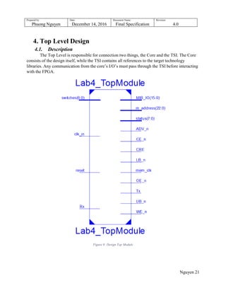
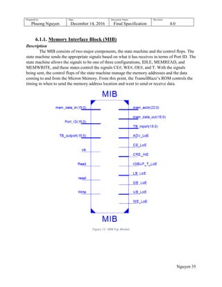
This document provides specifications for a System on Chip (SoC) design containing a Memory Interface Block (MIB) and a Universal Asynchronous Receiver and Transmitter (UART) interface. It includes block diagrams, I/O descriptions, state machines, and verification simulations for the top level design and all internal blocks. The top level interacts with a provided TramelBlaze microcontroller core and contains the MIB and UART blocks. The MIB allows the TramelBlaze to interface with an off-chip memory. The UART block contains independently designed transmit and receive engines that have been verified to successfully transmit and receive serial data to and from a terminal via the UART interface. Revision 4.0

![Prepared by:
Phuong Nguyen
Date:
December 14, 2016
Document Name:
Final Specification
Revision:
4.0
Nguyen 13
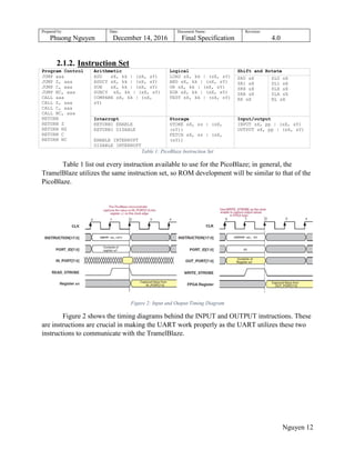
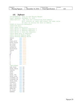
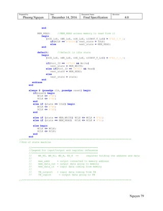
Instruction Description Function Zero Carry
ADD sX, kk Add sX with literal kk sX ← sX + kk ? ?
CALL aaa Unconditionally call subroutine at aaa TOS ← PC
PC ← aaa
- -
COMP sX, kk Compare sX with literal kk, Set CARRY and
ZERO flags as appropriate.
If sX=kk, ZERO ← 1
If sX<kk, CARRY ← 1
? ?
ENINT Enable interrupt input INTERRUPT_ENABLE ← 1 - -
FETCH sX, ss Read scratchpad RAM location ss into
register sX
sX ← RAM[ss] - -
INPUT sX, pp Read value on input port location pp into
register sX
PORT_ID ← pp
sX ← IN_PORT
- -
JUMP aaa Unconditionally jump to aaa PC ← aaa - -
JUMPZ aaa If ZERO flag set, jump to aaa If ZERO=1, PC ← aaa - -
LOAD sX, kk Load register sX with literal kk sX ← kk - -
OUTPUT sX, pp Write register sX to output port location
pp
PORT_ID ← pp
OUT_PORT ← sX
- -
RETEN Return from interrupt service routine. PC ← TOS
ZERO ← Preserved ZERO
CARRY ← Preserved CARRY
INTERRUPT_ENABLE ← 1
? ?
RETURN Unconditionally return from subroutine PC ← TOS+1 - -
STORE sX, (sY) Write register sX to scratchpad RAM
location pointed to by register sY
RAM[(sY)] ← sX - -
Table 2: Instructions used by Design
In the development of this design, many of the TramelBlaze‟s instructions were used to
create the ROM. Table 2 goes into detail with every instruction used in the development of the
UART.](https://image.slidesharecdn.com/6a2677cb-2966-481e-8a6c-00b20a1ce095-161224015254/85/Lab4_Report_460-13-320.jpg)
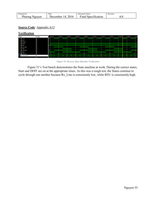
![Prepared by:
Phuong Nguyen
Date:
December 14, 2016
Document Name:
Final Specification
Revision:
4.0
Nguyen 24
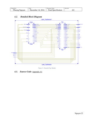
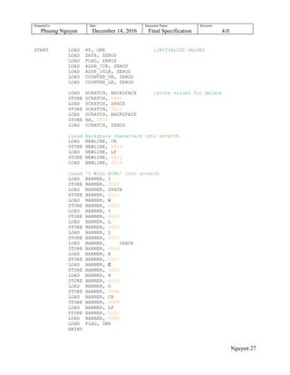
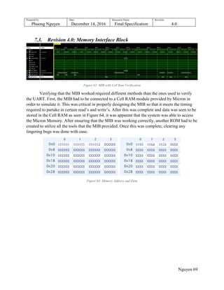
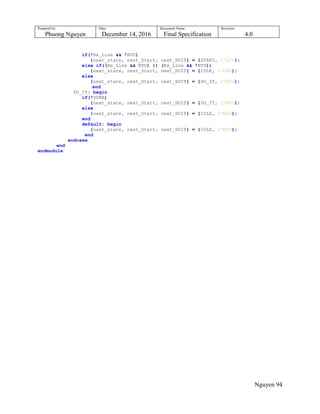
4.5.2. Pin Assignment
Input Signals Assignment Output Signals Assignment
clk_in E3 Tx_Out D4
reset E16 ADV_n T13
Rx_In C4 CE_n L18
Parity_ops [2] V6 LB_n J15
Parity_ops [1] V7 UB_n J13
Parity_ops [0] R5 OE_n H14
Baud_Selector [3] R6 WE_n R11
Baud_Selector [2] R7 CRE J14
Baud_Selector [1] U8 mem_clk T15
Baud_Selector [0] U9 Status [7] U6
Status [6] U7
Status [5] T4
Status [4] T5
Status [3] T6
Status [2] R8
Status [1] V9
Status [0] T8
Table 10: Top Level Pin Assignments
Address Bus Data Bus
m_address[22]: U13 m_address[13]: U16 m_address[4]: H16 MIB_IO[1]: P17 MIB_IO[6]: T18
m_address[21]: M16 m_address[12]: P14 m_address[3]: J17 MIB_IO[1]: N17 MIB_IO[5]: R17
m_address[20]: T10 m_address[11]: V12 m_address[2]: H15 MIB_IO[1]: P18 MIB_IO[4]: U18
m_address[19]: U17 m_address[10]: V14 m_address[1]: H17 MIB_IO[1]: M17 MIB_IO[3]: R13
m_address[18]: V17 m_address[9]: U14 m_address[0]: J18 MIB_IO[1]: M18 MIB_IO[2]: U12
m_address[17]: M13 m_address[8]: V16 MIB_IO[1]: G17 MIB_IO[1]: T11
m_address[16]: N16 m_address[7]: N15 MIB_IO[9]: G18 MIB_IO[0]: R12
m_address[15]: N14 m_address[6]: K13 MIB_IO[8]: F18
m_address[14]: R15 m_address[5]: K15 MIB_IO[7]: R18
Table 11: Memory Address and Bidirectional Data Ports
4.5.3. Electrical Characteristics
Switches
o 1.8V are considered Logical 1
o 0V are considered Logical 0
Buttons
o 3.3V are considered Logical 1
o 0V are considered Logical 0](https://image.slidesharecdn.com/6a2677cb-2966-481e-8a6c-00b20a1ce095-161224015254/85/Lab4_Report_460-24-320.jpg)
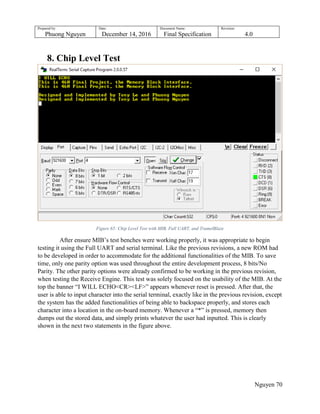
![Prepared by:
Phuong Nguyen
Date:
December 14, 2016
Document Name:
Final Specification
Revision:
4.0
Nguyen 31
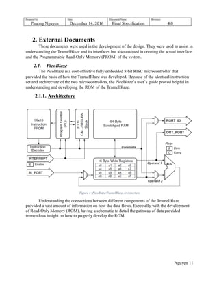
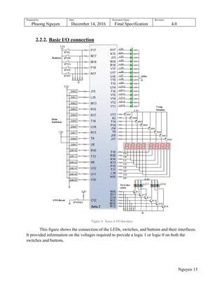
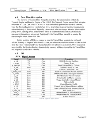
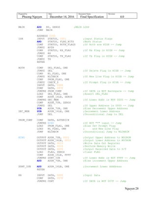
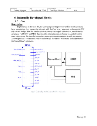
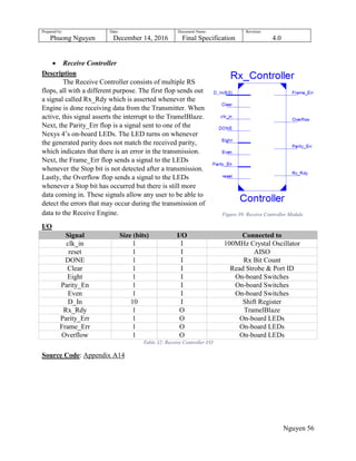
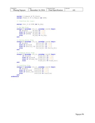
5. Externally Developed Blocks
5.1. Asynchronous In, Synchronous Out (AISO)
Description
This block ensures the reset to every
block‟s reset is synchronous to each other
hence the name. The reset of this block is
directly connected to a button (BTNC), which
when asserted will synchronously reset every
module.
I/O
Signal I/O Connected to
clk_in Input 100MHz Crystal Oscillator
reset Input BTNC
sync Output Every Block‟s Reset
Table 12: AISO I/O
Register Map
Register Usage Description
flop [1:0] Synchronize Upon reset, sends a single pulse to all modules
Table 13: AISO Register Map
Source Code: Appendix A17
Figure 10: AISO Block Diagram](https://image.slidesharecdn.com/6a2677cb-2966-481e-8a6c-00b20a1ce095-161224015254/85/Lab4_Report_460-31-320.jpg)
![Prepared by:
Phuong Nguyen
Date:
December 14, 2016
Document Name:
Final Specification
Revision:
4.0
Nguyen 32
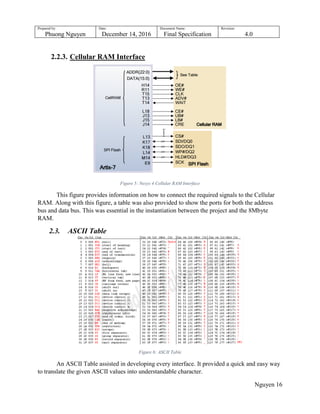
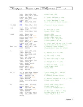
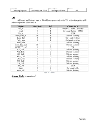
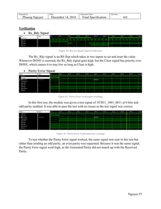
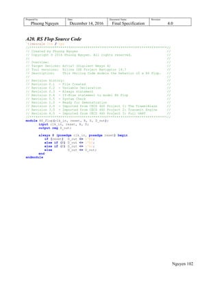
5.2. TramelBlaze
Description
The TramelBlaze is a 16-bit soft-
core microcontroller that emulates the
PicoBlaze. The TramelBlaze provides the
instantiation for a ROM, which it will read
from and perform actions based on the
instructions provided by the ROM. In this
application, the TramelBlaze utilize every
port in order to receive ASCII values and
to transmit ASCII values to a Serial
Terminal. The READ_STROBE and
WRITE_STROBE will be outputted to
UART which will help the UART
determine whether to use the Transmit or
Receive Engine during a specific operation.
I/O
Signal I/O Connected to
IN_PORT [15:0] Input UART
CLK Input 100MHz Crystal Oscillator
INTERRUPT Input RS Flop
RESET Input AISO
OUT_PORT [15:0] Output UART
PORT_ID [15:0] Output UART & In_Sel MUX
INTERRUPT_ACK Output RS Flop
READ_STROBE Output UART
WRITE_STROBE Output UART
Table 14: TramelBlaze I/O
Register Map
Register Usage Description
R[15:0] PROM Functions individually in TramelBlaze PROM
Table 15: TramelBlaze Register Map
Figure 11: TramelBlaze Block Diagram](https://image.slidesharecdn.com/6a2677cb-2966-481e-8a6c-00b20a1ce095-161224015254/85/Lab4_Report_460-32-320.jpg)
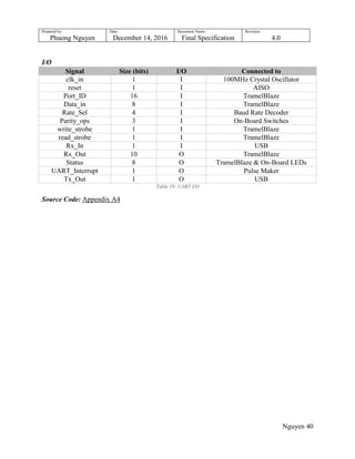
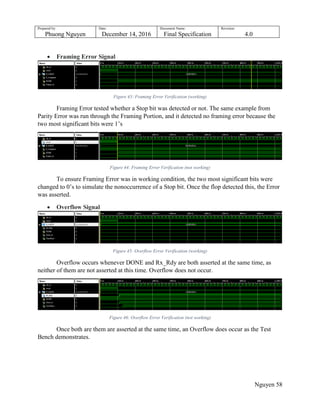
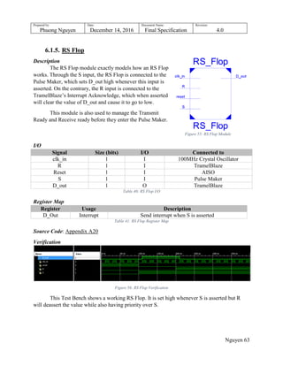
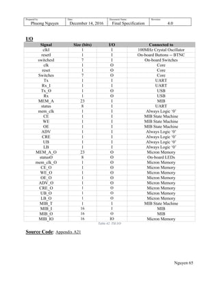
![Prepared by:
Phuong Nguyen
Date:
December 14, 2016
Document Name:
Final Specification
Revision:
4.0
Nguyen 43
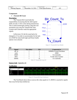
I/O
Signal Size (bits) I/O Connected to
clk_in 1 I 100MHz Crystal Oscillator
reset 1 I AISO
ld_in 1 I Write Strobe & Port ID
Baud_Rate 19 I Baud Rate Decoder
Data_in 8 I TramelBlaze
Parity_ops 3 I On-Board Switches
Tx_Rdy 1 I UART Interrupt
Tx_Out 1 I USB
Table 20: Transmit Engine I/O
Register Map
Register Module Description
count [18:0] Time_Counter Baud Rate Counter
count [3:0] Bit_Count Fixed number on how many times shift register can shift
Tx_Rdy Controller Acknowledge that Transmission is Ready
Load_D1 Controller Delays data to reach DoIt and Shift Register for one clock period
DoIt Controller Allows Bit Count and Bit Time Counter to increment
D_out [7:0] Controller Takes in Data from TramelBlaze
bit_10_9 Bit Decoder Determines what bit 10 and 9 of shift register will do
register [10:0] Shift Register Prepare data to be shifted out to a designated pin
SD0 Shift Register Takes in Data from TramelBlaze
Table 21: Transmit Engine Register Map
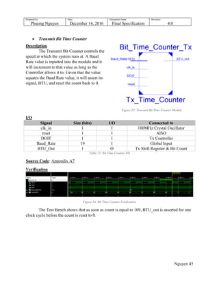
Source Code: Appendix A5
Verification
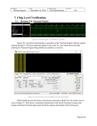
Figure 20: Transmit Engine Verification
The Transmit Engine is able to shift out data through the Tx_out line in accordance to the
requirements. This was done by giving the Transmit Engine different values, different Baud
Rates, and different Parity options to ensure that It was shifting out data properly.](https://image.slidesharecdn.com/6a2677cb-2966-481e-8a6c-00b20a1ce095-161224015254/85/Lab4_Report_460-43-320.jpg)
![Prepared by:
Phuong Nguyen
Date:
December 14, 2016
Document Name:
Final Specification
Revision:
4.0
Nguyen 47
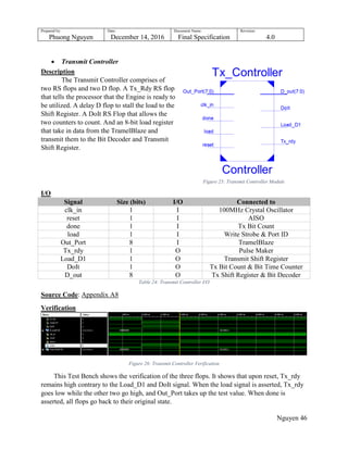
Bit Decoder
Description
The Bit Decoder determines the
values that will be placed in the 10th
and 9th
bit location of the Transmit Shift Register.
This is entirely based on the values of the
Eight, Parity Enable, and oHeL lines which
are taken directly from the Nexys 4‟s on-
board switches. Table 25 provides the True
Table logic for the decoder.
Eight Parity oHeL 10 9
0 0 0 1 1
0 0 1 1 1
0 1 0 1 ^Data [6:0]
0 1 1 1 ~^Data [6:0]
1 0 0 1 Data [7]
1 0 1 1 Data [7]
1 1 0 ^Data [7:0] Data [7]
1 1 1 ~^ Data [7:0] Data [7]
Table 25: Bit Decoder Truth Table
I/O
Signal Size (bits) I/O Connected to
Reg8_in 8 I Tx Controller
bits_parity_oHeL 3 I On-board Switches
bit_10_9 2 O Tx Shift Register
Table 26: Bit Decoder I/O
Source Code: Appendix A9
Verification
Figure 28: Bit Decoder Verification
This Test Bench proves how the different options work with the same data of 8H‟9E.
Figure 27: Bit Decoder Module](https://image.slidesharecdn.com/6a2677cb-2966-481e-8a6c-00b20a1ce095-161224015254/85/Lab4_Report_460-47-320.jpg)
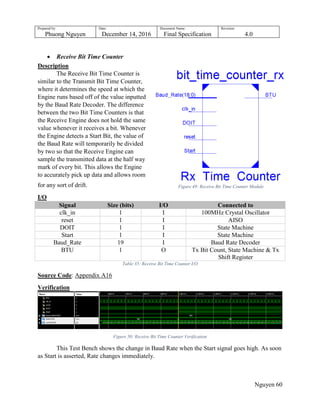
![Prepared by:
Phuong Nguyen
Date:
December 14, 2016
Document Name:
Final Specification
Revision:
4.0
Nguyen 51
I/O
Signal Size (bits) I/O Connected to
clk_in 1 I 100MHz Crystal Oscillator
reset 1 I AISO
Rx_In 1 I USB
Eight 1 I On-Board Switches
Parity_En 1 I On-Board Switches
oHeL 1 I On-Board Switches
read_strobe 1 I TramelBlaze
Rate 19 I Baud Rate Decoder
Port_ID 16 I TramelBlaze
Rx_Rdy 1 O UART Interrupt
Parity_Err 1 O On-Board LED
Frame_Err 1 O On-Board LED
Overflow 1 O On-Board LED
Rx_Data_TB 8 O TramelBlaze
Table 28: Receive Engine I/O
Register Map
Register Module Description
count [18:0] Rx Time Counter Baud Rate Counter
Start State Machine Detection of a Start bit
DOIT State Machine Allows Counter to count
State [1:0] State Machine Current position in receiving
next_state [1:0] State Machine Holds value of next state
next_Start State Machine Holds value of next Start
next_DOIT State Machine Holds value of next DOIT
count [3:0] Rx Bit Count Fixed number on how many times shift register can shift
bits [3:0] Rx Bit Count Based on Parity Options, determines compare value
Rx_Rdy Rx Controller Signify readiness to take in data
Parity_Err Rx Controller If asserted, generate Parity does not match received
Frame_Err Rx Controller Stop Bit not detected
Overflow Rx Controller Too much information
F_Check Rx Controller Holds last value received by Shift Register
Data_Ctrl [9:0] Rx Shift Register Data sent to Rx Controller
Data_TB [7:0] Rx Shift Register Data sent to TramelBlaze
Data_Out [9:0] Rx Shift Register Raw Data shifted from Transmitter
Table 29: Receive Engine Register Map
Source Code: Appendix A11](https://image.slidesharecdn.com/6a2677cb-2966-481e-8a6c-00b20a1ce095-161224015254/85/Lab4_Report_460-51-320.jpg)
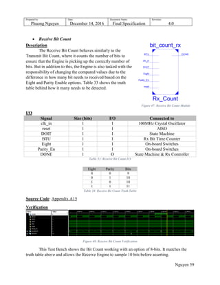
![Prepared by:
Phuong Nguyen
Date:
December 14, 2016
Document Name:
Final Specification
Revision:
4.0
Nguyen 61
6.1.3. Baud Rate Decoder
Description
The Baud Rate Decoder is a 4-bit
Decoder that determines the speed at which the
Transmit and Receive Engine run at.
I/O
Signal Size (bits) I/O Connected to
Rate_Sel 4 I R6, R7, U8, U9
Baud_Rate 19 O Transmit Engine
Table 36: Baud Rate Decoder I/O
Register Map
Register Usage Description
Baud_Rate
[18:0]
Constant Change the constant that Bit Time Counter compares to
Table 37: Baud Rate Decoder Register Map
Source Code: Appendix A17
Verification
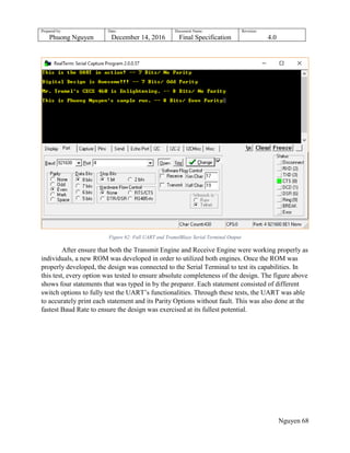
Figure 52: Baud Rate Decoder Verification
The Baud Rate Decoder proves that it is working properly by associating the correct
value with the correct switch orientation.
Figure 51: Baud Rate Decoder Module](https://image.slidesharecdn.com/6a2677cb-2966-481e-8a6c-00b20a1ce095-161224015254/85/Lab4_Report_460-61-320.jpg)
![Prepared by:
Phuong Nguyen
Date:
December 14, 2016
Document Name:
Final Specification
Revision:
4.0
Nguyen 62
6.1.4. Pulse Maker
Description
This block generates a one clock period
pulse whenever a signal is asserted. With two D
flops inside, it is able to take the signal and generate
a one clock period pulse to the output. In this
application, The D_in input will take in an interrupt
signal from the UART and it will set the Interrupt
through the pulse and sent it over to an RS flop,
which manages the interrupt of the TramelBlaze.
I/O
Signal Size (bits) I/O Connected to
clk_in 1 I 100MHz Crystal Oscillator
D_in 1 I UART
reset 1 I AISO
pulse 1 O RS Flop (S)
Table 38: Pulse Maker I/O
Register Map
Register Usage Description
flop [1:0] Pulse Create a one clock cycle pulse when flop [1:0] = [0, 1]
Table 39: Pulse Maker Register Map
Source Code: Appendix A19
Verification
Figure 54: Pulse Maker Verification
This Test bench proves that the Pulse Maker is working properly, it is only sends a one
clock period pulse regardless of how long the signal may be.
Figure 53: Pulse Maker Module](https://image.slidesharecdn.com/6a2677cb-2966-481e-8a6c-00b20a1ce095-161224015254/85/Lab4_Report_460-62-320.jpg)
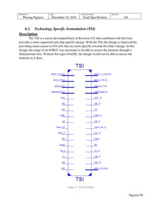
![Prepared by:
Phuong Nguyen
Date:
December 14, 2016
Document Name:
Final Specification
Revision:
4.0
Nguyen 71
9. Appendix
The Appendix includes the Verilog code to every module developed or mentioned in this
report with the exception of the TramelBlaze.
A1. Top Module Source Code
`timescale 1ns / 1ps
//***********************************************************************//
// Class: CECS 460 - System on Chip Design //
// Project name: Final SOC Specification //
// File name: Lab4_TopModule.v //
// //
// Created by Phuong Nguyen //
// Copyright © 2016 Phuong Nguyen. All rights reserved. //
// //
// Overview: //
// Target Devices: Artix7 (Digilent Nexys 4) //
// Tool versions: Xilinx ISE Project Navigator 14.7 //
// Description: This is the project's top module. It instantiates the //
// Core and the TSI into one module. //
// //
// Revision History: //
// Revision 0.1 - File Created //
// Revision 0.2 - Variable Declaration //
// Revision 0.3 - Wire Declaration //
// Revision 0.4 - Instantiation of Core and TSI //
// Revision 0.5 - Test Benched //
// - Nexys 4 Test //
// Revision 1.0 - Ready for Demonstration //
//***********************************************************************//
module Lab4_TopModule(clk_in, reset, switches,
Rx, Tx,
m_address, status, CE_n, WE_n, OE_n, ADV_n, CRE, UB_n, LB_n,
mem_clk, MIB_IO
);
//FPGA Connection
input clk_in, reset;
input [6:0] switches;
wire c_clk, c_reset;
wire [6:0] c_switches;
//UART Connection
input Rx;
wire c_Tx, c_Rx;
output Tx;
//MIB Connection
wire [22:0] c_mem_addr;
wire [7:0] c_status;
wire c_CE, c_WE, c_OE, c_ADV, c_CRE, c_UB, c_LB;
wire c_mem_clk;
output [22:0] m_address;
output [7:0] status;
output CE_n, WE_n, OE_n, ADV_n, CRE, UB_n, LB_n;
output mem_clk;
output [15:0] MIB_IO;](https://image.slidesharecdn.com/6a2677cb-2966-481e-8a6c-00b20a1ce095-161224015254/85/Lab4_Report_460-71-320.jpg)
![Prepared by:
Phuong Nguyen
Date:
December 14, 2016
Document Name:
Final Specification
Revision:
4.0
Nguyen 72
wire [15:0] MIB_I, MIB_O;
wire T;
//INPUTS: clk_in, reset, Rx_In, [15:0] mem_data_in, [3:0] Baud_Sel,
// [2:0] Parity_ops;
//OUTPUTS: [22:0] mem_addr, [15:0] mem_data_out, IOBUF_T_LoE;
// CE_LoE, WE_LoE, OE_LoE, ADV_LoE, CRE_HiE, UB_LoE, LB_LoE;
// Tx_Out, [7:0] Status, mem_clk
Core Core(
.clk_in(c_clk),
.reset(c_reset),
.Rx_In(c_Rx), //From TSI -- Micro USB
.mem_data_in(MIB_O), //From TSI -- IOBUF
.Baud_Sel(c_switches[3:0]), //From TSI -- Switches
.Parity_ops(c_switches[6:4]), //From TSI -- Switches
.mem_addr(c_mem_addr), //To TSI -- Micron Memory
.mem_data_out(MIB_I), //To TSI -- IOBUF
.IOBUF_T_LoE(T), //To TSI -- IOBUF
.CE_LoE(c_CE), //To TSI -- Micron Memory
.WE_LoE(c_WE), //To TSI -- Micron Memory
.OE_LoE(c_OE), //To TSI -- Micron Memory
.ADV_LoE(c_ADV), //To TSI -- always "0"
.CRE_HiE(c_CRE), //To TSI -- always "0"
.UB_LoE(c_UB), //To TSI -- always "0"
.LB_LoE(c_LB), //To TSI -- always "0"
.Tx_Out(c_Tx), //To TSI -- Micro USB
.Status(c_status), //To TSI -- LEDs
.mem_clk(c_mem_clk) //To TSI -- Micron Memory
);
//FPGA Inputs
//INPUTS: clkI, resetI, [6:0] switchesI, Tx, Rx_I,
// [22:0] MEM_A, [7:0] status, CE, WE, OE, ADV, CRE, UB, LB
// MIB_T, [15:0] MIB_I
//OUTPUTS: clk, reset, [6:0] switches, Tx_O, Rx
// [22:0] MEM_A_O, [7:0] statusO, CE_O, WE_O, OE_O, ADV_O,
// CRE_O, UB_O, LB_O
// [15:0] MIB_O
//INOUTS: [15:0] MIB_IO
TSI TSI (
.clkI(clk_in), //Global In -- System Clock
.resetI(reset), //Global In -- Reset
.switchesI(switches), //Global In -- Switches
.clk(c_clk), //To Core -- System Clock
.reset(c_reset), //To Core -- Reset
.switches(c_switches), //To Core -- Switches
.Tx(c_Tx), //From Core -- Transmit Engine
.Rx_I(Rx), //Global In -- Receive Engine
.Tx_O(Tx), //Global Out -- Transmit Engine
.Rx(c_Rx), //To Core -- Receive Engine
.MEM_A(c_mem_addr), //From Core -- MIB
.status(c_status), //From Core -- Statuses
.mem_clk(c_mem_clk), //From Core -- Top
.CE(c_CE), //From Core -- MIB
.WE(c_WE), //From Core -- MIB
.OE(c_OE), //From Core -- MIB](https://image.slidesharecdn.com/6a2677cb-2966-481e-8a6c-00b20a1ce095-161224015254/85/Lab4_Report_460-72-320.jpg)
![Prepared by:
Phuong Nguyen
Date:
December 14, 2016
Document Name:
Final Specification
Revision:
4.0
Nguyen 74
A2. Core Source Code
`timescale 1ns / 1ps
//***********************************************************************//
// Class: CECS 460 - System on Chip Design //
// Project name: Final SOC Specification //
// File name: Core.v //
// //
// Created by Phuong Nguyen //
// Copyright © 2016 Phuong Nguyen. All rights reserved. //
// //
// Overview: //
// Target Devices: Artix7 (Digilent Nexys 4) //
// Tool versions: Xilinx ISE Project Navigator 14.7 //
// Description: The Core contains the instantiation of design's //
// processor, its interfaces, and its accessory modules. //
// //
// Revision History: //
// Revision 0.1 - File Created //
// Revision 0.2 - Variable Declaration //
// Revision 0.3 - Wire Declaration //
// Revision 1.0 - Imported from CECS 460 Project 3: Full UART //
// Revision 1.1 - Name change to Core //
// Revision 1.2 - Instantiation of MIB //
// - Modification of conditional assignment //
// - MIB variables declared //
// Revision 1.3 - Creation of mem_clk conditional assignment //
// Revision 1.4 - Test Benched //
// Revision 2.0 - Ready for Demonstration //
//***********************************************************************//
module Core(clk_in, reset, Rx_In, mem_data_in, Baud_Sel, Parity_ops,
mem_addr, mem_data_out, IOBUF_T_LoE, CE_LoE, WE_LoE, OE_LoE,
ADV_LoE, CRE_HiE, UB_LoE, LB_LoE, Tx_Out, Status, mem_clk,
);
input clk_in, reset, Rx_In;
input [15:0] mem_data_in;
input [3:0] Baud_Sel;
input [2:0] Parity_ops;
output [22:0] mem_addr;
output [15:0] mem_data_out;
output IOBUF_T_LoE;
output wire CE_LoE, WE_LoE, OE_LoE, ADV_LoE, CRE_HiE, UB_LoE, LB_LoE;
output wire Tx_Out;
output wire [7:0] Status;
output wire mem_clk;
wire [15:0] TB_In, TB_inport;
wire [15:0] Port_ID;
wire [15:0] TB_outport;
wire [7:0] Rx_Data;
wire reset_sync;
wire write_strobe, read_strobe, UART_Int;
wire Pulse, Interrupt, Interrupt_Ack;
wire ld_in, In_Sel;
assign mem_clk = 1'b0;](https://image.slidesharecdn.com/6a2677cb-2966-481e-8a6c-00b20a1ce095-161224015254/85/Lab4_Report_460-74-320.jpg)
![Prepared by:
Phuong Nguyen
Date:
December 14, 2016
Document Name:
Final Specification
Revision:
4.0
Nguyen 75
assign ld_in = write_strobe && (Port_ID == 16'b0000); //To Tx_Engine
assign TB_In = (Port_ID == 16'h0001) ? {8'b0, Status}:
(Port_ID == 16'h0000) ? {8'b0, Rx_Data}:
(Port_ID == 16'h0014) ? TB_inport:
16'b0;
//INPUTS: clk_in, reset, Read, Write, [15:0] Port_ID, [15:0] mem_data_in,
// [15:0] TB_outport
//OUTPUTS: CE_LoE, WE_LoE, OE_LoE, IOBUF_T_LoE, ADV_LoE, CRE_HiE, UB_LoE,
// LB_LoE, [22:0] mem_addr, [15:0] mem_data_out, [15:0] TB_inport;
MIB MIB (.clk(clk_in),
.reset(reset),
.Port_ID(Port_ID), //From TramelBlaze
.Read(read_strobe), //From TramelBlaze
.Write(write_strobe), //From TramelBlaze
.TB_outport(TB_outport), //From TramelBlaze
.mem_data_in(mem_data_in), //Global -- To TSI
.CE_LoE(CE_LoE), //Global -- To Memory
.WE_LoE(WE_LoE), //Global -- To Memory
.OE_LoE(OE_LoE), //Global -- To Memory
.IOBUF_T_LoE(IOBUF_T_LoE), //Global -- To TSI
.ADV_LoE(ADV_LoE), //Global -- To Memory
.CRE_HiE(CRE_HiE), //Global -- To Memory
.UB_LoE(UB_LoE), //Global -- To Memory
.LB_LoE(LB_LoE), //Global -- To Memory
.mem_addr(mem_addr), //Global -- To Memory
.mem_data_out(mem_data_out), //Global -- To TSI
.TB_inport(TB_inport) //From TramelBlaze
);
//INPUTS: clk_in, reset, *Port_ID, *****Data_In, **Rate_Sel,
// ***Parity_ops, write_strobe, read_strobe, Rx_In,
//OUTPUTS: ****Rx_Data_TB, *****Status, UART_Interrupt, Tx_Out
//*[15:0], **[3:0], ***[2:0], ****[9:0], *****[7:0];
UART_Top UART(.clk_in(clk_in),
.reset(reset_sync),
.Port_ID(Port_ID), //From TramelBlaze
.Data_In(TB_outport), //From TramelBlaze
.Rate_Sel(Baud_Sel), //Global Input – Switches
.Parity_ops(Parity_ops), //Global Input – Switches
.write_strobe(write_strobe), //From TramelBlaze
.read_strobe(read_strobe), //From TramelBlaze
.Rx_In(Rx_In), //From USB***
.Interrupt_Ack(Interrupt_Ack), //From TramelBlaze
.ld_in(ld_in), //From Assign Statement
.Rx_Data_TB(Rx_Data), //To TramelBlaze
.Status(Status), //Global Output
.UART_Interrupt(UART_Int), //To Pulse Maker
.Tx_Out(Tx_Out) //To USB
);
//INPUTS: CLK, RESET, *IN_PORT, INTERRUPT,
//OUTPUTS: *OUT_PORT, *PORT_ID, READ_STROBE, WRITE_STROBE, INTERRUPT_ACK
//*[15:0]
tramelblaze_top TramelBlaze (.CLK(clk_in),
.RESET(reset_sync),
.IN_PORT(TB_In), //From UART,
.INTERRUPT(Interrupt), //From RS Flop
.OUT_PORT(TB_outport), //To UART
.PORT_ID(Port_ID), //To UART, MIB](https://image.slidesharecdn.com/6a2677cb-2966-481e-8a6c-00b20a1ce095-161224015254/85/Lab4_Report_460-75-320.jpg)
![Prepared by:
Phuong Nguyen
Date:
December 14, 2016
Document Name:
Final Specification
Revision:
4.0
Nguyen 77
A3. MIB Source Code
`timescale 1ns / 1ps
//***********************************************************************//
// Class: CECS 460 - System on Chip Design //
// Project name: Final SOC Specification //
// File name: MIB.v //
// //
// Created by Tony Le & Phuong Nguyen //
// Copyright © 2016 Tony Le & Phuong Nguyen. All rights reserved. //
// //
// Overview: //
// Target Devices: Artix7 (Digilent Nexys 4) //
// Tool versions: Xilinx ISE Project Navigator 14.7 //
// Description: The MIB sends signals to the Micron Memory as it //
// receives data and sends data to it based on the //
// signals. //
// //
// Revision History: //
// Revision 0.1 - File Created //
// Revision 0.2 - Variable Declaration //
// Revision 0.3 - Wire Declaration //
// Revision 0.4 - Creation of State Machine //
// Revision 0.5 - Creation of Control Flops //
// Revision 0.6 - Changes to Clock Counter //
// Revision 0.7 - Test Benched with Cell Ram Module //
// Revision 0.8 - Changes to RD_R flop //
// Revision 1.0 - Ready for Demonstration //
//***********************************************************************//
module MIB(clk, reset, Port_ID, Read, Write, //LoE = Low Enable
TB_outport, mem_data_in, //HiE = High Enable
CE_LoE, WE_LoE, OE_LoE, IOBUF_T_LoE,
ADV_LoE, CRE_HiE, UB_LoE, LB_LoE,
mem_addr, mem_data_out, TB_inport
);
input clk, reset;
input Read, Write;
input [15:0] Port_ID;
input [15:0] mem_data_in;
input [15:0] TB_outport;
//control lines
output reg CE_LoE, WE_LoE, OE_LoE, IOBUF_T_LoE; //signal depends on state
output reg ADV_LoE, CRE_HiE, UB_LoE, LB_LoE; //signal will always be 1'b0
//output data signals
output reg [22:0] mem_addr;
output reg [15:0] mem_data_out;
output reg [15:0] TB_inport;
reg [3:0] state, next_state;
reg [3:0] WCLK, RCLK; //counter for read and write state
wire write_done, read_done; //done signal for write and read state
reg nCE_LoE, nWE_LoE, nOE_LoE, nIOBUF_T_LoE; //next state command signal
reg nADV_LoE, nCRE_HiE, nUB_LoE, nLB_LoE;](https://image.slidesharecdn.com/6a2677cb-2966-481e-8a6c-00b20a1ce095-161224015254/85/Lab4_Report_460-77-320.jpg)
![Prepared by:
Phuong Nguyen
Date:
December 14, 2016
Document Name:
Final Specification
Revision:
4.0
Nguyen 78
//internal registers holding the addr and data
reg [6:0] WA_R0;
reg [15:0] WA_R1, WD_R;
reg [15:0] RD_R;
parameter //control word parameter
IDLE = 4'h0,
MEM_WRITE = 4'h1,
MEM_READ = 4'h2,
//operation word parameter
WADDR1 = 16'h11,
WADDR2 = 16'h12,
WDATA = 16'h13,
RDATA = 16'h14,
MEMREAD = 16'h15,
MEMWRITE = 16'h16;
//************************************************************************************
//Control Word Present state logic
always @(posedge clk, posedge reset) begin
if(reset)
begin
state <= IDLE; //reset to idle state
//because low polarity, resets to one
{CE_LoE, WE_LoE, OE_LoE, IOBUF_T_LoE} <= 4'b1_1_1_1;
//signal always 0
{ADV_LoE, CRE_HiE, UB_LoE, LB_LoE} <= 4'b0_0_0_0;
end
else
begin
state <= next_state;
{CE_LoE, WE_LoE, OE_LoE, IOBUF_T_LoE} <=
{nCE_LoE, nWE_LoE, nOE_LoE, nIOBUF_T_LoE};
end
end
//Control Word Next State Logic
always @ (*) begin
case(state)
IDLE: //idle state not accessing memory
begin
{nCE_LoE, nWE_LoE, nOE_LoE, nIOBUF_T_LoE} = 4'b1_1_1_1;
if((Port_ID == 16'h16) && Write) //condition to write
next_state = MEM_WRITE;
else if(Port_ID == 16'h15 && Read) //condition to read
next_state = MEM_READ;
else
next_state = IDLE;
end
MEM_WRITE: //MEM_WRITE access memory to write into it
begin
{nCE_LoE, nWE_LoE, nOE_LoE, nIOBUF_T_LoE} = 4'b0_0_1_0;
if(WCLK == 4'b1100) next_state = IDLE;
else next_state = MEM_WRITE;](https://image.slidesharecdn.com/6a2677cb-2966-481e-8a6c-00b20a1ce095-161224015254/85/Lab4_Report_460-78-320.jpg)
![Prepared by:
Phuong Nguyen
Date:
December 14, 2016
Document Name:
Final Specification
Revision:
4.0
Nguyen 80
//start of operation logic
always @ (posedge clk, posedge reset)
if(reset) begin
WA_R0 <= 7'h0;
WA_R1 <= 16'h0;
WD_R <= 16'h0;
mem_addr <= 16'h0;
mem_data_out <= 16'h0;
TB_inport <= 16'h0;
end
else
case(Port_ID)
WADDR1: if(Write) WA_R0 <= TB_outport[6:0];
else WA_R0 <= WA_R0;
WADDR2: if(Write) WA_R1 <= TB_outport;
else WA_R1 <= WA_R1;
WDATA: if(Write) WD_R <= TB_outport;
else WD_R <= WD_R;
RDATA: TB_inport <= RD_R;
MEMREAD: if(Read)
mem_addr <= {WA_R0, WA_R1};
else
mem_addr <= mem_addr;
MEMWRITE: if(Write) begin
mem_addr <= {WA_R0, WA_R1};
mem_data_out <= WD_R;
end
else begin
mem_addr <= mem_addr;
mem_data_out <= mem_data_out;
end
default: begin
WA_R0 <= WA_R0;
WA_R1 <= WA_R1;
WD_R <= WD_R;
mem_addr <= mem_addr;
mem_data_out <= mem_data_out;
TB_inport <= TB_inport;
end
endcase
always @ (posedge clk, posedge reset)
if(reset) RD_R <= 16'h0000;
else if(RCLK == 4'b1011) RD_R <= mem_data_in;
else RD_R <= RD_R;
endmodule](https://image.slidesharecdn.com/6a2677cb-2966-481e-8a6c-00b20a1ce095-161224015254/85/Lab4_Report_460-80-320.jpg)
![Prepared by:
Phuong Nguyen
Date:
December 14, 2016
Document Name:
Final Specification
Revision:
4.0
Nguyen 81
A4. UART Top Source Code
`timescale 1ns / 1ps
//***********************************************************************//
// Class: CECS 460 - System on Chip Design //
// Project name: Final SOC Specification //
// File name: UART.v //
// //
// Created by Phuong Nguyen //
// Copyright © 2016 Phuong Nguyen . All rights reserved. //
// //
// Overview: //
// Target Devices: Artix7 (Digilent Nexys 4) //
// Tool versions: Xilinx ISE Project Navigator 14.7 //
// Description: The Universal Asynchronous Receiver and Transmitter //
// instantiates the Transmit Engine, Receive Engine and //
// Baud Rate Decoder together. //
// //
// Revision History: //
// Revision 0.1 - File Created //
// Revision 0.2 - Variable Declaration //
// Revision 0.3 - Assign statement for Tx Load, UART Interrupt //
// Revision 0.4 - Concatenate Statuses and Tx_Rdy and Rx_Rdy //
// Revision 1.0 - Ready for Demonstration //
// Revision 2.0 - Imported from CECS 460 Project 3: Full UART //
//***********************************************************************//
module UART_Top(clk_in, reset, Port_ID, Data_In, Rate_Sel, Parity_ops,
write_strobe, read_strobe, Rx_In, Interrupt_Ack, ld_in,
Rx_Data_TB, Status, UART_Interrupt, Tx_Out);
input clk_in, reset;
input [15:0] Port_ID;
input [7:0] Data_In;
input [3:0] Rate_Sel;
input [2:0] Parity_ops;
input write_strobe, read_strobe;
input Rx_In, Interrupt_Ack;
input ld_in;
output [7:0] Rx_Data_TB, Status;
output UART_Interrupt, Tx_Out;
wire [18:0] B_Rate;
wire Rx_Rdy, Tx_Rdy, Rx_RS, Tx_RS;
wire PERR, FERR, OVF;
assign UART_Interrupt = Rx_Rdy || Tx_Rdy; //Global Output
assign Status = {3'b0, OVF, FERR, PERR, Tx_Rdy, Rx_Rdy}; //Global Output
//INPUTS: clk_in, reset, ld_in, [18:0] Baud_Rate, [7:0] Data_in,
// [2:0] Parity_ops;
//OUTPUTS: Tx_Rdy, Tx_Out;
Tx_Engine_Top Tx_Engine (.clk_in(clk_in),
.reset(reset),
.ld_in(ld_in), //Global Input
.Baud_Rate(B_Rate), //From Baud Decoder
.Data_in(Data_In), //Global Input -- TramelBlaze
.Parity_ops(Parity_ops), //Global Input -- Switches
.Tx_Rdy(Tx_RS), //To Transmit RS Flop
.Tx_Out(Tx_Out) //Global Output](https://image.slidesharecdn.com/6a2677cb-2966-481e-8a6c-00b20a1ce095-161224015254/85/Lab4_Report_460-81-320.jpg)
![Prepared by:
Phuong Nguyen
Date:
December 14, 2016
Document Name:
Final Specification
Revision:
4.0
Nguyen 82
);
//INPUT: clk_in, reset, R, S;
//OUTPUT: D_out;
RS_Flop Transmit_RS (.clk_in(clk_in),
.reset(reset),
.R(Interrupt_Ack),
.S(Tx_RS),
.D_out(Tx_Rdy)
);
//INPUTS: clk_in, reset, Rx_In, Eight, Parity_En, oHeL, read_strobe,
// [18:0] Rate, [15:0] Port_ID,
//OUTPUTS: Rx_Rdy, Parity_Err, Frame_Err, Overflow, [7:0] Rx_Data_TB
Rx_Engine_Top Rx_Engine (.clk_in(clk_in),
.reset(reset),
.Rx_In(Rx_In), //Global Input -- USB
.Eight(Parity_ops[2]), //Global Input -- Switches
.Parity_En(Parity_ops[1]), //Global Input -- Switches
.oHeL(Parity_ops[0]), //Global Input -- Switches
.read_strobe(read_strobe), //Global Input -- TB
.Rate(B_Rate), //From Baud Decoder
.Port_ID(Port_ID), //Global Input -- TB
.Rx_Rdy(Rx_RS), //To Status & Receive RS
.Parity_Err(PERR), //To Status
.Frame_Err(FERR), //To Status
.Overflow(OVF), //To Status
.Rx_Data_TB(Rx_Data_TB) //Global Output
);
//INPUT: clk_in, reset, R, S;
//OUTPUT: D_out;
RS_Flop Receive_RS (.clk_in(clk_in),
.reset(reset),
.R(Interrupt_Ack),
.S(Rx_RS),
.D_out(Rx_Rdy)
);
//INPUTS: [3:0] Rate_Sel
//OUTPUTS: [18:0] Baud_Rate
Baud_Decoder Baud_Rate (.Rate_Sel(Rate_Sel), //Global Input -- Switches
.Baud_Rate(B_Rate) //To Tx and Rx Engine
);
endmodule](https://image.slidesharecdn.com/6a2677cb-2966-481e-8a6c-00b20a1ce095-161224015254/85/Lab4_Report_460-82-320.jpg)
![Prepared by:
Phuong Nguyen
Date:
December 14, 2016
Document Name:
Final Specification
Revision:
4.0
Nguyen 83
A5. Transmit Engine Top Source Code
`timescale 1ns / 1ps
//***********************************************************************//
// Created by Phuong Nguyen //
// Copyright © 2016 Phuong Nguyen. All rights reserved. //
// //
// Overview: //
// Target Devices: Artix7 (Digilent Nexys 4) //
// Tool versions: Xilinx ISE Project Navigator 14.7 //
// Description: This module instantiates the Tx Engine together. //
// It connects thes Bit Count, Bit Time Counter, //
// Controller and Shift Register together. //
// //
// Revision History: //
// Revision 0.1 - File Created //
// Revision 0.2 - Variable Declaration //
// Revision 0.3 - Wire Declaration //
// Revision 0.4 - Instantiate all Modules //
// Revision 0.5 - Test Benched //
// Revision 1.0 - Ready for Demonstration //
// Revision 2.0 - Imported from CECS 460 Project 2: Transmit Engine //
// Revision 3.0 - Imported from CECS 460 Project 3: Full UART //
//***********************************************************************//
module Tx_Engine_Top(clk_in, reset, ld_in, Baud_Rate, Data_in, Parity_ops,
Tx_Rdy, Tx_Out);
input clk_in, reset, ld_in;
input [18:0] Baud_Rate;
input [7:0] Data_in;
input [2:0] Parity_ops;
output Tx_Rdy, Tx_Out;
wire [7:0] Reg_out;
wire DoIt, done;
wire Load_D1;
wire BTU;
wire [1:0] bit_10_9;
//INPUTS: clk_in, reset, DOIT, BTU
//OUTPUTS: DONE
Bit_Count_Tx Tx_Count (.clk_in(clk_in),
.reset(reset),
.DOIT(DoIt),
.BTU(BTU),
.DONE(done)
);
//INPUTS: clk_in, reset, DOIT, Baud_Rate*
//OUTPUTS: BTU_out
//*[18:0]
Bit_Time_Counter_Tx Tx_Time_Counter (.clk_in(clk_in),
.reset(reset),
.DOIT(DoIt),
.Baud_Rate(Baud_Rate),
.BTU_out(BTU)
);
//INPUTS: clk_in, reset, done, load, Out_Port*
//OUTPUTS: Tx_rdy, Load_D1, DoIt, D_out*](https://image.slidesharecdn.com/6a2677cb-2966-481e-8a6c-00b20a1ce095-161224015254/85/Lab4_Report_460-83-320.jpg)
![Prepared by:
Phuong Nguyen
Date:
December 14, 2016
Document Name:
Final Specification
Revision:
4.0
Nguyen 84
//*[7:0]
Tx_Controller Controller (.clk_in(clk_in),
.reset(reset),
.done(done),
.load(ld_in),
.Out_Port(Data_in),
.Tx_rdy(Tx_Rdy),
.Load_D1(Load_D1),
.DoIt(DoIt),
.D_out(Reg_out)
);
//INPUTS: Reg8_in*, bits_parity_oHeL**
//OUTPUTS: bit_10_9***
//*[7:0] **[2:0] ***[1:0]
Bit_10_9_Decoder Bit_Decoder (.Reg8_in(Reg_out),
.bits_parity_oHeL(Parity_ops),
.bit_10_9(bit_10_9)
);
//INPUTS: clk_in, reset, load, shift_en, S_Data_in, D_in*
//OUTPUTS: SD0
//*[10:0]
Shift_Register_Tx Tx_Shift_Reg (.clk_in(clk_in),
.reset(reset),
.load(Load_D1),
.shift_en(BTU),
.S_Data_in(1'b1),
.D_in({bit_10_9, Reg_out[6:0], 2'b01}),
.SD0(Tx_Out)
);
endmodule](https://image.slidesharecdn.com/6a2677cb-2966-481e-8a6c-00b20a1ce095-161224015254/85/Lab4_Report_460-84-320.jpg)
![Prepared by:
Phuong Nguyen
Date:
December 14, 2016
Document Name:
Final Specification
Revision:
4.0
Nguyen 85
A6. Transmit Bit Count Source Code
`timescale 1ns / 1ps
//***********************************************************************//
// Created by Phuong Nguyen //
// Copyright © 2016 Phuong Nguyen. All rights reserved. //
// //
// Overview: //
// Target Devices: Artix7 (Digilent Nexys 4) //
// Tool versions: Xilinx ISE Project Navigator 14.7 //
// Description: This module will count the number of times the shift //
// register shifts through. It ensures that the shift //
// register does not shift pass 11 times. //
// //
// Revision History: //
// Revision 0.1 - File Created //
// Revision 0.2 - Variable Declaration //
// Revision 0.3 - Assign statement & Sequential Logic //
// Revision 0.4 - Test Benched //
// Revision 1.0 - Ready for Demonstration //
// Revision 2.0 - Imported from CECS 460 Project 2: Transmit Engine //
// Revision 3.0 - Imported from CECS 460 Project 3: Full UART //
//***********************************************************************//
module Bit_Count_Tx(clk_in, reset, DOIT, BTU, DONE);
input clk_in, reset;
input DOIT, BTU;
output DONE;
reg [3:0] count;
// Pulse when count is 11
assign DONE = (count == 12);
always @(posedge clk_in, posedge reset) begin
if(reset) count <= 4'b0;
else if(DONE) count <= 4'b0;
else
case({DOIT, BTU})
2'b00: count <= 4'b0;
2'b01: count <= 4'b0;
2'b10: count <= count;
2'b11: count <= count + 4'b1;
endcase
end
endmodule](https://image.slidesharecdn.com/6a2677cb-2966-481e-8a6c-00b20a1ce095-161224015254/85/Lab4_Report_460-85-320.jpg)
![Prepared by:
Phuong Nguyen
Date:
December 14, 2016
Document Name:
Final Specification
Revision:
4.0
Nguyen 86
A7. Transmit Bit Time Counter Source Code
`timescale 1ns / 1ps
//***********************************************************************//
// Created by Phuong Nguyen //
// Copyright © 2016 Phuong Nguyen. All rights reserved. //
// //
// Overview: //
// Target Devices: Artix7 (Digilent Nexys 4) //
// Tool versions: Xilinx ISE Project Navigator 14.7 //
// Description: The Bit Time Counter determines the speed at which //
// the Transmit Engine will run at. It will continuously //
// count to a given Baud Rate Count and assert its //
// output //
// //
// Revision History: //
// Revision 0.1 - File Created //
// Revision 0.2 - Variable Declaration //
// Revision 0.3 - Assign and Always statement //
// Revision 1.0 - Ready for Demonstration //
// Revision 2.0 - Imported from CECS 460 Project 2: Transmit Engine //
// Revision 3.0 - Imported from CECS 460 Project 3: Full UART //
//***********************************************************************//
module Bit_Time_Counter_Tx(clk_in, reset, DOIT, Baud_Rate, BTU_out);
input clk_in, reset;
input DOIT;
input [18:0] Baud_Rate;
output wire BTU_out;
reg [18:0] count;
// Pulse when count is 11
assign BTU_out = (count == Baud_Rate);
always @(posedge clk_in, posedge reset) begin
if(reset) count <= 19'b0;
else if(BTU_out) count <= 19'b0; else
case({DOIT, BTU_out})
2'b00: count <= 19'b0;
2'b01: count <= 19'b0;
2'b10: count <= count + 19'b1;
2'b11: count <= 19'b0;
default: count <= count;
endcase
end
endmodule](https://image.slidesharecdn.com/6a2677cb-2966-481e-8a6c-00b20a1ce095-161224015254/85/Lab4_Report_460-86-320.jpg)
![Prepared by:
Phuong Nguyen
Date:
December 14, 2016
Document Name:
Final Specification
Revision:
4.0
Nguyen 87
A8. Transmit Controller Source Code
`timescale 1ns / 1ps
//***********************************************************************//
// Created by Phuong Nguyen //
// Copyright © 2016 Phuong Nguyen. All rights reserved. //
// //
// Overview: //
// Target Devices: Artix7 (Digilent Nexys 4) //
// Tool versions: Xilinx ISE Project Navigator 14.7 //
// Description: Tx_Controller consists of all the necessary flop in //
// order to dictate the Tx Engine's workings. //
// //
// Revision History: //
// Revision 0.1 - File Created //
// Revision 0.2 - Variable Declaration //
// Revision 0.3 - Sequential Logic for all flops //
// Revision 0.4 - Correction to Tx_Rdy flop //
// Revision 0.5 - Test Benched //
// Revision 1.0 - Ready for Demonstration //
// Revision 2.0 - Imported from CECS 460 Project 2: Transmit Engine //
// Revision 3.0 - Imported from CECS 460 Project 3: Full UART //
//***********************************************************************//
module Tx_Controller(clk_in, reset, done, load, Out_Port, Tx_rdy, Load_D1,
DoIt, D_out);
input clk_in, reset, done, load;
input [7:0] Out_Port;
output reg Tx_rdy, Load_D1, DoIt;
output reg [7:0] D_out;
// Tx_rdy RS flop (reverse logic)
always @ (posedge clk_in, posedge reset) begin
if(reset) Tx_rdy <= 1'b1;
else if (load) Tx_rdy <= 1'b0;
else if (done) Tx_rdy <= 1'b1;
else Tx_rdy <= Tx_rdy;
end
// D Flip Flop output to DoIt and Shift Reg
always @ (posedge clk_in, posedge reset) begin
if(reset) Load_D1 <= 1'b0;
else Load_D1 <= load;
end
// DoIt RS flop
always @ (posedge clk_in, posedge reset) begin
if(reset) DoIt <= 1'b0;
else if(done) DoIt <= 1'b0;
else if(Load_D1) DoIt <= 1'b1;
else DoIt <= DoIt;
end
// Out_Port Load Register
always @ (posedge clk_in, posedge reset) begin
if(reset) D_out <= 8'b0;
else if(load) D_out <= Out_Port;
else D_out <= D_out;
end
endmodule](https://image.slidesharecdn.com/6a2677cb-2966-481e-8a6c-00b20a1ce095-161224015254/85/Lab4_Report_460-87-320.jpg)
![Prepared by:
Phuong Nguyen
Date:
December 14, 2016
Document Name:
Final Specification
Revision:
4.0
Nguyen 88
A9. Transmit Bit 10 & 9 Decoder Source Code
`timescale 1ns / 1ps
//***********************************************************************//
// Created by Phuong Nguyen //
// Copyright © 2016 Phuong Nguyen. All rights reserved. //
// //
// Overview: //
// Target Devices: Artix7 (Digilent Nexys 4) //
// Tool versions: Xilinx ISE Project Navigator 14.7 //
// Description: This Decoder will determine the values that go into //
// bits 10 and 9, it can be an 8th bit, or a parity //
// depending on the user's input. //
// //
// Revision History: //
// Revision 0.1 - File Created //
// Revision 0.2 - Variable Declaration //
// Revision 0.3 - Decode Logic //
// Revision 0.4 - Test Benched //
// Revision 1.0 - Ready for Demonstration //
// Revision 2.0 - Imported from CECS 460 Project 2: Transmit Engine //
// Revision 3.0 - Imported from CECS 460 Project 3: Full UART //
//***********************************************************************//
module Bit_10_9_Decoder(Reg8_in, bits_parity_oHeL, bit_10_9);
input [7:0] Reg8_in;
input [2:0] bits_parity_oHeL;
output reg [1:0] bit_10_9;
always @ (*) begin
case (bits_parity_oHeL)
3'b000: bit_10_9 <= 2'b11;
3'b001: bit_10_9 <= 2'b11;
3'b010: bit_10_9 <= {1'b1, ^Reg8_in[6:0]};
3'b011: bit_10_9 <= {1'b1, ~^Reg8_in[6:0]};
3'b100: bit_10_9 <= {1'b1, Reg8_in[7]};
3'b101: bit_10_9 <= {1'b1, Reg8_in[7]};
3'b110: bit_10_9 <= {^Reg8_in[7:0], Reg8_in[7]};
3'b111: bit_10_9 <= {~^Reg8_in[7:0], Reg8_in[7]};
default: bit_10_9 <= 2'b11;
endcase
end
endmodule](https://image.slidesharecdn.com/6a2677cb-2966-481e-8a6c-00b20a1ce095-161224015254/85/Lab4_Report_460-88-320.jpg)
![Prepared by:
Phuong Nguyen
Date:
December 14, 2016
Document Name:
Final Specification
Revision:
4.0
Nguyen 89
A10. Transmit Shift Register Source Code
`timescale 1ns / 1ps
//***********************************************************************//
// Created by Phuong Nguyen //
// Copyright © 2016 Phuong Nguyen. All rights reserved. //
// //
// Overview: //
// Target Devices: Artix7 (Digilent Nexys 4) //
// Tool versions: Xilinx ISE Project Navigator 14.7 //
// Description: The shift register will take in data from the bit //
// decoder and the controller register and appropriately //
// shift bit outs one by one. //
// //
// Revision History: //
// Revision 0.1 - File Created //
// Revision 0.2 - Variable Declaration //
// Revision 0.3 - Sequential Logic Design for Shift Register //
// Revision 0.4 - Test Benched //
// Revision 1.0 - Ready for Demonstration //
// Revision 2.0 - Imported from CECS 460 Project 2: Transmit Engine //
// Revision 3.0 - Imported from CECS 460 Project 3: Full UART //
//***********************************************************************//
module Shift_Register_Tx(clk_in, reset, load, shift_en, S_Data_in, D_in, SD0);
input clk_in, reset, load, shift_en, S_Data_in;
input [10:0] D_in;
output reg SD0;
reg [10:0] register;
always @ (posedge clk_in, posedge reset) begin
if(reset) begin
register <= 11'h7FF;
SD0 <= 1'b1;
end
else if (load) register <= D_in;
else if (shift_en) begin
register <= {S_Data_in, register[10:1]};
SD0 <= register[0];
end
else begin
register <= register;
SD0 <= SD0;
end
end
endmodule](https://image.slidesharecdn.com/6a2677cb-2966-481e-8a6c-00b20a1ce095-161224015254/85/Lab4_Report_460-89-320.jpg)
![Prepared by:
Phuong Nguyen
Date:
December 14, 2016
Document Name:
Final Specification
Revision:
4.0
Nguyen 90
A11: Receive Engine Top Source Code
`timescale 1ns / 1ps
//***********************************************************************//
// Created by Phuong Nguyen //
// Copyright © 2016 Phuong Nguyen. All rights reserved. //
// //
// Overview: //
// Target Devices: Artix7 (Digilent Nexys 4) //
// Tool versions: Xilinx ISE Project Navigator 14.7 //
// Description: This module instantiates the Rx Engine together. //
// It connects the Shift Register, State Machine, //
// Controller, Bit Count, Bit Time Counter. //
// //
// Revision History: //
// Revision 0.1 - File Created //
// Revision 0.2 - Variable Declaration //
// Revision 0.3 - Wire Declaration //
// Revision 0.4 - Instantiate Shift Register, State Machine, Controller,//
// - Bit Count and Bit Timer Counter //
// Revision 0.5 - Tx Line fed into Rx Line //
// Revision 1.0 - Ready for Demonstration //
// Revision 2.0 - Imported from CECS 460 Project 3: Full UART //
//***********************************************************************//
module Rx_Engine_Top(clk_in, reset, Rx_In, Eight, Parity_En, oHeL, read_strobe,
Rate, Port_ID, Rx_Rdy, Parity_Err, Frame_Err, Overflow,
Rx_Data_TB);
input clk_in, reset, Rx_In, Eight, Parity_En, oHeL, read_strobe;
input [18:0] Rate;
input [15:0] Port_ID;
output Rx_Rdy, Parity_Err, Frame_Err, Overflow;
output [7:0] Rx_Data_TB;
wire [9:0] Data_Ctrl;
wire BTU, Start;
wire DONE, DOIT;
wire Clear;
assign Clear = read_strobe && (Port_ID == 16'b0000);
//INPUTS: clk_in, reset, BTU, Start, Rx_In, DONE, Eight, Parity_En,
//OUTPUTS: *Data_Ctrl, **Data_TB
//*[9:0], ** [7:0]
Shift_Register_Rx Rx_Shift_Reg (.clk_in(clk_in),
.reset(reset),
.BTU(BTU), //From Bit Time Counter
.Start(Start), //From FSM
.Rx_In(Rx_In), //Global Input
.Eight(Eight), //Global Input
.Parity_En(Parity_En), //Global Input
.Data_Ctrl(Data_Ctrl), //To Controller
.Data_TB(Rx_Data_TB) //Global Out
);
//INPUTS: clk_in, reset, Rx_Line, BTU, DONE;
//OUTPUTS: Start, DOIT
Rx_FSM State_Machine (.clk_in(clk_in),
.reset(reset),
.Rx_Line(Rx_In), //Global Output](https://image.slidesharecdn.com/6a2677cb-2966-481e-8a6c-00b20a1ce095-161224015254/85/Lab4_Report_460-90-320.jpg)
![Prepared by:
Phuong Nguyen
Date:
December 14, 2016
Document Name:
Final Specification
Revision:
4.0
Nguyen 91
.BTU(BTU), //From Bit Time Counter
.DONE(DONE), //From Bit Count
.Start(Start), //To Shift Register and Time Counter
.DOIT(DOIT) //To Bit Count and Bit Time Counter
);
//INPUTS: clk_in, reset, DONE, Clear, Eight, Parity_En, Even, *D_In;
//OUTPUTS: Rx_Rdy, Parity_Err, Frame_Err, Overflow;
//*[9:0]
Rx_Controller Controller(.clk_in(clk_in),
.reset(reset),
.DONE(DONE), //From Bit Count
.Clear(Clear), //Global Input
.Eight(Eight), //Global Input
.Parity_En(Parity_En), //Global Input
.Even(!oHeL), //Global Input
.D_In(Data_Ctrl), //From Shift Register
.Rx_Rdy(Rx_Rdy), //Global Output
.Parity_Err(Parity_Err), //Global Output
.Frame_Err(Frame_Err), //Global Output
.Overflow(Overflow) //Global Output
);
//INPUTS: clk_in, reset, DOIT, BTU, Eight, Parity_En
//OUTPUTS: DONE
bit_count_rx Rx_Count(.clk_in(clk_in),
.reset(reset),
.DOIT(DOIT), //From FSM
.BTU(BTU), //From Bit Time Counter
.Eight(Eight), //Global Input
.Parity_En(Parity_En), //Global Input
.DONE(DONE) //To FSM, Controller,
);
//INPUTS: clk_in, reset, DOIT, Start, Baud_Rate*
//OUTPUTS: BTU
//*[18:0]
bit_time_counter_rx Rx_Time_Counter(.clk_in(clk_in),
.reset(reset),
.DOIT(DOIT), //From FSM
.Start(Start), //From FSM
.Baud_Rate(Rate), //Global Input
.BTU(BTU) //To FSM,SR, Bit Counter
);
endmodule](https://image.slidesharecdn.com/6a2677cb-2966-481e-8a6c-00b20a1ce095-161224015254/85/Lab4_Report_460-91-320.jpg)
![Prepared by:
Phuong Nguyen
Date:
December 14, 2016
Document Name:
Final Specification
Revision:
4.0
Nguyen 92
A12: Receive Shift Register Source Code
`timescale 1ns / 1ps
//***********************************************************************//
// Created by Phuong Nguyen //
// Copyright © 2016 Phuong Nguyen. All rights reserved. //
// //
// Overview: //
// Target Devices: Artix7 (Digilent Nexys 4) //
// Tool versions: Xilinx ISE Project Navigator 14.7 //
// Description: This module acts as the data receive of the Receive //
// Engine, any data gets shifted into this module before //
// it goes to any other modules //
// //
// Revision History: //
// Revision 0.1 - File Created //
// Revision 0.2 - Variable Declaration //
// Revision 0.3 - Wire Declaration //
// Revision 0.4 - Create Shift Register Block //
// Revision 0.5 - Create assign statement //
// Revision 0.6 - Changed Combinational Block Behavior //
// Revision 0.7 - Test Benched, Verified //
// Revision 1.0 - Ready for Demonstration //
// Revision 2.0 - Imported from CECS 460 Project 3: Full UART //
//***********************************************************************//
module Shift_Register_Rx(clk_in, reset, BTU, Start, Rx_In, Eight, Parity_En,
Data_Ctrl, Data_TB);
input clk_in, reset, BTU, Start, Rx_In;
input Eight, Parity_En;
output reg [9:0] Data_Ctrl;
output reg [7:0] Data_TB;
reg [9:0] Data_Out;
wire Shift_En;
assign Shift_En = BTU && !Start;
/***Raw Data shifted in***/
always @ (posedge clk_in, posedge reset) begin
if(reset) Data_Out <= 10'b0;
else if (Shift_En) Data_Out <= {Rx_In, Data_Out[9:1]};
else Data_Out <= Data_Out;
end
always @ (*) begin
case ({Eight, Parity_En})
2'b00:{Data_Ctrl, Data_TB} <= {2'b0, Data_Out[9:2], 1'b0, Data_Out[8:2]};
2'b01:{Data_Ctrl, Data_TB} <= {1'b0, Data_Out[9:1], 1'b0, Data_Out[7:1]};
2'b10:{Data_Ctrl, Data_TB} <= {1'b0, Data_Out[9:1], Data_Out[8:1]};
2'b11:{Data_Ctrl, Data_TB} <= {1'b0, Data_Out[8:0], Data_Out[7:0]};
default:{Data_Ctrl, Data_TB} <= Data_Out;
endcase
end
endmodule](https://image.slidesharecdn.com/6a2677cb-2966-481e-8a6c-00b20a1ce095-161224015254/85/Lab4_Report_460-92-320.jpg)
![Prepared by:
Phuong Nguyen
Date:
December 14, 2016
Document Name:
Final Specification
Revision:
4.0
Nguyen 93
A13. Receive State Machine Source Code
`timescale 1ns / 1ps
//***********************************************************************//
// Created by Phuong Nguyen //
// Copyright © 2016 Phuong Nguyen. All rights reserved. //
// //
// Overview: //
// Target Devices: Artix7 (Digilent Nexys 4) //
// Tool versions: Xilinx ISE Project Navigator 14.7 //
// Description: This module detects the Start bit of the data //
// received and allows the counters to work when it is //
// detected. The state machine will allow the counter to //
// keep counting up until the counter send a signal to //
// signify its completion of data reception. //
// //
// Revision History: //
// Revision 0.1 - File Created //
// Revision 0.2 - Variable Declaration //
// Revision 0.3 - Wire Declaration //
// Revision 0.4 - Create Next State Logic Block //
// Revision 0.5 - Create Present State Combinational Block //
// Revision 0.6 - Changed FSM State Machine to Modified Moore //
// Revision 0.7 - Test Benched, Verified //
// Revision 1.0 - Ready for Demonstration //
// Revision 2.0 - Imported from CECS 460 Project 3: Full UART //
//***********************************************************************//
module Rx_FSM(clk_in, reset, Rx_Line, BTU, DONE, Start, DOIT);
input clk_in, reset;
input Rx_Line, BTU, DONE;
output reg Start, DOIT;
reg [1:0] state, next_state;
reg next_Start, next_DOIT;
parameter IDLE = 0, START = 1, DO_IT = 2;
/***Next State Logic***/
always @ (posedge clk_in, posedge reset) begin
if(reset) begin
state <= IDLE;
Start <= 1'b0;
DOIT <= 1'b0;
end
else begin
state <= next_state;
Start <= next_Start;
DOIT <= next_DOIT;
end
end
/***Present State Logic***/
always @ (*) begin
case (state)
IDLE: begin
if(Rx_Line)
{next_state, next_Start, next_DOIT} = {IDLE, 2'b00};
else
{next_state, next_Start, next_DOIT} = {START, 2'b11};
end
START: begin](https://image.slidesharecdn.com/6a2677cb-2966-481e-8a6c-00b20a1ce095-161224015254/85/Lab4_Report_460-93-320.jpg)
![Prepared by:
Phuong Nguyen
Date:
December 14, 2016
Document Name:
Final Specification
Revision:
4.0
Nguyen 95
A14. Receive Controller Source Code
`timescale 1ns / 1ps
//***********************************************************************//
// Created by Phuong Nguyen //
// Copyright © 2016 Phuong Nguyen. All rights reserved. //
// //
// Overview: //
// Target Devices: Artix7 (Digilent Nexys 4) //
// Tool versions: Xilinx ISE Project Navigator 14.7 //
// Description: The controller determines the parity of the data //
// received by the receive engine. At the same time, //
// this module sends a signal to denote that it is ready //
// to receive data. //
// //
// Revision History: //
// Revision 0.1 - File Created //
// Revision 0.2 - Variable Declaration //
// Revision 0.3 - Wire Declaration //
// Revision 0.4 - Create Sequential Logic Blocks for parities //
// Revision 0.5 - Create Combinational Block for parity logic //
// Revision 0.6 - Test Benched, Verified //
// Revision 1.0 - Ready for Demonstration //
// Revision 2.0 - Imported from CECS 460 Project 3: Full UART //
//***********************************************************************//
module Rx_Controller(clk_in, reset, DONE, Clear, Eight, Parity_En, Even, D_In,
Rx_Rdy, Parity_Err, Frame_Err, Overflow);
input clk_in, reset, DONE, Clear, Eight, Parity_En, Even;
input [9:0] D_In;
output reg Rx_Rdy, Parity_Err, Frame_Err, Overflow;
//Parity Error Wiring
wire P_REC, Bit8, P_XOR, P_GEN, GEN_REC, Parity_In;
// Framing Error Wiring
reg F_Check;
wire F_Compare, Frame_In;
// Overflow Wiring
wire Over_In;
// Parity Error Set Logic
assign P_REC = Eight ? D_In[8] : D_In[7];
assign Bit8 = Eight ? D_In[7] : 1'b0;
assign P_XOR = ^{Bit8, D_In[6:0]};
assign P_GEN = Even ? P_XOR : !P_XOR;
assign GEN_REC = ^{P_GEN, P_REC};
assign Parity_In = Parity_En && GEN_REC && DONE;
// Framing Error Set Logic
always @ (*) begin
case ({Eight, Parity_En})
2'b00: F_Check = D_In[7];
2'b01: F_Check = D_In[8];
2'b10: F_Check = D_In[8];
2'b11: F_Check = D_In[9];
default: F_Check = D_In[7];
endcase
end](https://image.slidesharecdn.com/6a2677cb-2966-481e-8a6c-00b20a1ce095-161224015254/85/Lab4_Report_460-95-320.jpg)
![Prepared by:
Phuong Nguyen
Date:
December 14, 2016
Document Name:
Final Specification
Revision:
4.0
Nguyen 97
A15: Receive Bit Count Source Code
`timescale 1ns / 1ps
//***********************************************************************//
// Created by Phuong Nguyen //
// Copyright © 2016 Phuong Nguyen. All rights reserved. //
// //
// Overview: //
// Target Devices: Artix7 (Digilent Nexys 4) //
// Tool versions: Xilinx ISE Project Navigator 14.7 //
// Description: This module counts the bits received by the receive //
// engine, it is all determined by the values set in //
// the eight and parity enable options on the on-board //
// switches. //
// //
// Revision History: //
// Revision 0.1 - File Created //
// Revision 0.2 - Variable Declaration //
// Revision 0.3 - Wire Declaration //
// Revision 0.4 - Create Sequential Logic for Counter //
// Revision 0.5 - Create MUX based on Eight and Parity Enable //
// Revision 0.6 - Modification of MUX values //
// Revision 1.0 - Ready for Demonstration //
// Revision 2.0 - Imported from CECS 460 Project 3: Full UART //
//***********************************************************************//
module bit_count_rx(clk_in, reset, DOIT, BTU, Eight, Parity_En, DONE);
input clk_in, reset, DOIT, BTU;
input Eight, Parity_En;
output DONE;
reg [3:0] count, bits;
assign DONE = (count == bits);
always @ (posedge clk_in, posedge reset) begin
if (reset) count <= 4'b0;
else if (DONE) count <= 4'b0;
else begin
case ({DOIT, BTU})
2'b00: count <= 4'b0;
2'b01: count <= 4'b0;
2'b10: count <= count;
2'b11: count <= count + 4'b1;
default: count <= count;
endcase
end
end
always @ (*) begin
case ({Eight, Parity_En})
2'b00: bits = 9;
2'b01: bits = 10;
2'b10: bits = 10;
2'b11: bits = 11;
default: bits = 9;
endcase
end
endmodule](https://image.slidesharecdn.com/6a2677cb-2966-481e-8a6c-00b20a1ce095-161224015254/85/Lab4_Report_460-97-320.jpg)
![Prepared by:
Phuong Nguyen
Date:
December 14, 2016
Document Name:
Final Specification
Revision:
4.0
Nguyen 98
A16: Receive Bit Time Counter Source Code
`timescale 1ns / 1ps
//***********************************************************************//
// Created by Phuong Nguyen //
// Copyright © 2016 Phuong Nguyen. All rights reserved. //
// //
// Overview: //
// Target Devices: Artix7 (Digilent Nexys 4) //
// Tool versions: Xilinx ISE Project Navigator 14.7 //
// Description: Similar to the bit time counter of the transmit, this //
// time counter differs by the way it halves its baud //
// rate whenever a Start bit is detected by the state //
// machine, this allows the receive engine to pick up //
// data at the half way mark of each bit. //
// //
// Revision History: //
// Revision 0.1 - File Created //
// Revision 0.2 - Variable Declaration //
// Revision 0.3 - Wire Declaration //
// Revision 0.4 - Create Sequential Logic Block for Counter //
// Revision 0.5 - Create assign statement to change Baud Rate //
// Revision 1.0 - Ready for Demonstration //
//***********************************************************************//
module bit_time_counter_rx(clk_in, reset, DOIT, Start, Baud_Rate, BTU);
input clk_in, reset, DOIT, Start;
input [18:0] Baud_Rate;
output wire BTU;
reg [18:0] count;
wire [18:0] Rate;
assign BTU = (count == Rate);
assign Rate = Start ? (Baud_Rate >> 1): Baud_Rate;
always @ (posedge clk_in, posedge reset) begin
if (reset) count <= 19'b0;
else if (BTU) count <= 19'b0;
else begin
case ({DOIT, BTU})
2'b00: count <= 19'b0;
2'b01: count <= 19'b0;
2'b10: count <= count + 19'b1;
2'b11: count <= 19'b0;
default: count <= count;
endcase
end
end
endmodule](https://image.slidesharecdn.com/6a2677cb-2966-481e-8a6c-00b20a1ce095-161224015254/85/Lab4_Report_460-98-320.jpg)
![Prepared by:
Phuong Nguyen
Date:
December 14, 2016
Document Name:
Final Specification
Revision:
4.0
Nguyen 99
A17. Baud Rate Decoder Source Code
`timescale 1ns / 1ps
//***********************************************************************//
// Created by Phuong Nguyen //
// Copyright © 2016 Phuong Nguyen. All rights reserved. //
// //
// Overview: //
// Target Devices: Artix7 (Digilent Nexys 4) //
// Tool versions: Xilinx ISE Project Navigator 14.7 //
// Description: The Baud Decoder will determine the speed at which //
// the transmit engine will run. The given values will //
// be sent to the Bit Time Counter which dictates the //
// speed. //
// //
// Revision History: //
// Revision 0.1 - File Created //
// Revision 0.2 - Variable Declaration //
// Revision 0.3 - Decode Logic for Baud Rate //
// Revision 0.4 - Test Benched //
// Revision 1.0 - Ready for Demonstration //
// Revision 2.0 - Imported from CECS 460 Project 2: Transmit Engine //
// Revision 3.0 - Imported from CECS 460 Project 3: Full UART //
//***********************************************************************//
module Baud_Decoder(Rate_Sel, Baud_Rate);
input [3:0] Rate_Sel;
output reg [18:0] Baud_Rate;
//Decode the Baud Rate
always @ (*) begin
case (Rate_Sel)
4'b0000: Baud_Rate = 333333; //300
4'b0001: Baud_Rate = 83333; //1200
4'b0010: Baud_Rate = 41667; //2400
4'b0011: Baud_Rate = 20833; //4800
4'b0100: Baud_Rate = 10417; //9600
4'b0101: Baud_Rate = 5208; //19200
4'b0110: Baud_Rate = 2604; //38400
4'b0111: Baud_Rate = 1736; //57600
4'b1000: Baud_Rate = 868; //115200
4'b1001: Baud_Rate = 434; //230400
4'b1010: Baud_Rate = 217; //460800
4'b1011: Baud_Rate = 109; //921600
default: Baud_Rate = 0;
endcase
end
endmodule](https://image.slidesharecdn.com/6a2677cb-2966-481e-8a6c-00b20a1ce095-161224015254/85/Lab4_Report_460-99-320.jpg)
![Prepared by:
Phuong Nguyen
Date:
December 14, 2016
Document Name:
Final Specification
Revision:
4.0
Nguyen 100
A18. AISO Source Code
`timescale 1ns / 1ps
//***********************************************************************//
// Created by John Tramel //
// Copyright © 2016 John Tramel. All rights reserved. //
// //
// Overview: //
// Target Devices: Artix7 (Digilent Nexys 4) //
// Tool versions: Xilinx ISE Project Navigator 14.7 //
// Description: AISO known better as Asynchronous In, Synchronous Out //
// will synchronize the reset for all modules so that //
// everything runs at the same time. //
// //
// Revision History: //
// Revision 0.1 - File Created //
// Revision 0.2 - Variable Declaration //
// Revision 0.3 - Assign and Always statement //
// Revision 1.0 - Ready for Demonstration //
// Revision 2.0 - Imported from CECS 360 Project 1: Up Down Counter //
// Revision 3.0 - Imported from CECS 460 Project 1: The TramelBlaze //
// Revision 4.0 - Imported from CECS 460 Project 2: Transmit Engine //
// Revision 5.0 - Imported from CECS 460 Project 3: Full UART //
//***********************************************************************//
module AISO(clk_in, reset, sync);
input clk_in, reset;
output sync;
reg [1:0] flop;
assign sync = ~flop[1];
always @ (posedge clk_in, posedge reset) begin
if (reset)
flop <= 2'b0;
else
flop <= {flop[0], 1'b1}; //flop[1] gets flop[0]
end //flop[0] gets 1'b1
endmodule](https://image.slidesharecdn.com/6a2677cb-2966-481e-8a6c-00b20a1ce095-161224015254/85/Lab4_Report_460-100-320.jpg)
![Prepared by:
Phuong Nguyen
Date:
December 14, 2016
Document Name:
Final Specification
Revision:
4.0
Nguyen 101
A19. Pulse Maker Source Code
`timescale 1ns / 1ps
//***********************************************************************//
// Created by Phuong Nguyen //
// Copyright © 2016 Phuong Nguyen. All rights reserved. //
// //
// Overview: //
// Target Devices: Artix7 (Digilent Nexys 4) //
// Tool versions: Xilinx ISE Project Navigator 14.7 //
// Description: This module functions to create pulses based on when //
// a debounced mechanical switch is pressed. It consists //
// of two flops that will output a pulse whenever one of //
// the flops is on and the other is off //
// //
// Revision History: //
// Revision 0.1 - File Created //
// Revision 0.2 - Variable Declaration //
// - Creation of two flops and always statement //
// Revision 0.3 - Correction on syntax of register //
// - Syntax Check //
// Revision 1.0 - Ready for Demonstration //
// Revision 2.0 - Imported from CECS 460 Project 1: The TramelBlaze //
// Revision 3.0 - Imported from CECS 460 Project 2: Transmit Engine //
// Revision 4.0 - Imported from CECS 460 Project 3: Full UART //
//***********************************************************************//
module pulse_maker(clk_in, reset, D_in, pulse);
input clk_in, reset, D_in;
output pulse;
reg [1:0] flop;
assign pulse = ~flop[1] && flop[0];
always @ (posedge clk_in, posedge reset) begin
if(reset) flop <= 2'b0;
else flop <= {flop[0], D_in};
end
endmodule](https://image.slidesharecdn.com/6a2677cb-2966-481e-8a6c-00b20a1ce095-161224015254/85/Lab4_Report_460-101-320.jpg)
![Prepared by:
Phuong Nguyen
Date:
December 14, 2016
Document Name:
Final Specification
Revision:
4.0
Nguyen 103
A21. TSI Source Code
`timescale 1ns / 1ps
//***********************************************************************//
// Created by Phuong Nguyen //
// Copyright © 2016 Phuong Nguyen. All rights reserved. //
// //
// Overview: //
// Target Devices: Artix7 (Digilent Nexys 4) //
// Tool versions: Xilinx ISE Project Navigator 14.7 //
// Description: The TSI handles all the inputs and outputs coming in //
// and out of the Core. //
// //
// Revision History: //
// Revision 0.1 - File Created //
// Revision 0.2 - Variable Declaration //
// Revision 0.3 - IOBUF, IBUF, OBUF, and IBUYF Created //
// Revision 0.4 - Test Benched with Project 3 Code //
// Revision 1.0 - Ready for Demonstration //
//***********************************************************************//
module TSI(clkI, resetI, switchesI,
clk, reset, switches,
Tx, Rx_I,
Tx_O, Rx,
MEM_A, status, mem_clk, CE, WE, OE, ADV, CRE, UB, LB,
MEM_A_O, statusO, mem_clk_O, CE_O, WE_O, OE_O, ADV_O, CRE_O, UB_O, LB_O,
MIB_T, MIB_I, MIB_O, MIB_IO);
//FPGA Inputs
input clkI; //System Clock
input resetI; //Global Reset
input [6:0] switchesI; //Baud Rate & Parity Ops
//Output to Core
output clk;
output reset;
output [6:0] switches;
//UART Interface
input Tx, Rx_I; //Core inputs
output Tx_O, Rx; //FPGA outputs
//Inputs from Core
input [22:0] MEM_A; //Memory Address
input [7:0] status; //Statuses
input mem_clk;
input CE; //Chip Enable
input WE; //Write Enable
input OE; //Output Enable
input ADV;
input CRE;
input UB;
input LB;
//Outputs to FPGA
output [22:0] MEM_A_O;
output [7:0] statusO;
output mem_clk_O;
output CE_O;
output WE_O;](https://image.slidesharecdn.com/6a2677cb-2966-481e-8a6c-00b20a1ce095-161224015254/85/Lab4_Report_460-103-320.jpg)
![Prepared by:
Phuong Nguyen
Date:
December 14, 2016
Document Name:
Final Specification
Revision:
4.0
Nguyen 104
output OE_O;
output ADV_O;
output CRE_O;
output UB_O;
output LB_O;
//dq
input MIB_T;
input [15:0] MIB_I;
output [15:0] MIB_O;
inout [15:0] MIB_IO;
//Dedicated Input Clock Buffer
IBUFG #(
.IOSTANDARD("DEFAULT")
)
Sys_Clk (
.O(clk), //To Core
.I(clkI) //From Top Level Port
);
//System Reset
IBUF #(
.IOSTANDARD("DEFAULT")
)
Sys_Reset(
.O(reset), //To Core
.I(resetI) //From Top Level Port
);
//UART Interface
OBUF #(
.IOSTANDARD("DEFAULT")
)
Transmit(
.O(Tx_O), //To Core
.I(Tx) //From Top Level Port
);
IBUF #(
.IOSTANDARD("DEFAULT")
)
Receive(
.O(Rx), //To Core
.I(Rx_I) //From Top Level Port
);
//Memory Address
OBUF #(
.IOSTANDARD("DEFAULT")
)
MEM_ADDR [22:0](
.O(MEM_A_O[22:0]), //Out to Micron
.I(MEM_A[22:0]) //From Core
);](https://image.slidesharecdn.com/6a2677cb-2966-481e-8a6c-00b20a1ce095-161224015254/85/Lab4_Report_460-104-320.jpg)
, //To FPGA LEDs
.I(status[7:0]) //From Core
);
//Switches buffer
IBUF #(
.IOSTANDARD("DEFAULT")
)
Iswitches [6:0](
.O(switches [6:0]), //To FPGA Switches
.I(switchesI [6:0]) //From Top Level Port
);
OBUF #(
.IOSTANDARD("DEFAULT")
)
mem_clk_out(
.O(mem_clk_O), //Out to Micron
.I(1'b0) //From Core
);
//Memory Signal Interface
OBUF #(
.IOSTANDARD("DEFAULT")
)
CE_LoE(
.O(CE_O), //Out to Micron
.I(CE) //From Core
);
OBUF #(
.IOSTANDARD("DEFAULT")
)
WE_LoE(
.O(WE_O), //Out to Micron
.I(WE) //From Core
);
OBUF #(
.IOSTANDARD("DEFAULT")
)
OE_LoE(
.O(OE_O), //Out to Micron
.I(OE) //From Core
);
OBUF #(
.IOSTANDARD("DEFAULT")
)](https://image.slidesharecdn.com/6a2677cb-2966-481e-8a6c-00b20a1ce095-161224015254/85/Lab4_Report_460-105-320.jpg)
, //buffer input into the module
.IO(MIB_IO[15:0]), //buffer inout port
.I(MIB_I[15:0]), //output value from the module
.T(MIB_T) //output when T is low
);
endmodule](https://image.slidesharecdn.com/6a2677cb-2966-481e-8a6c-00b20a1ce095-161224015254/85/Lab4_Report_460-106-320.jpg)