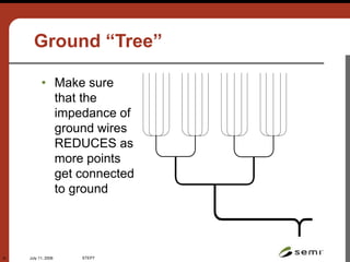
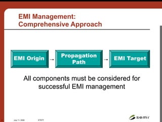
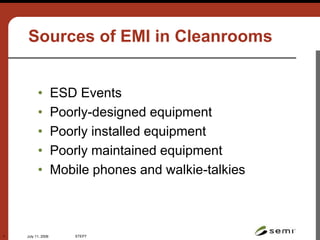
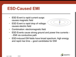
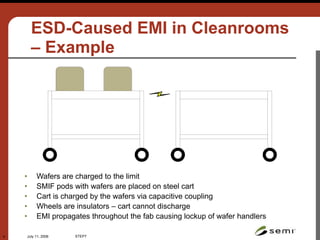
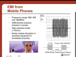
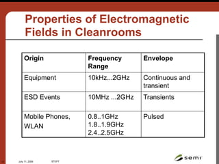
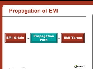
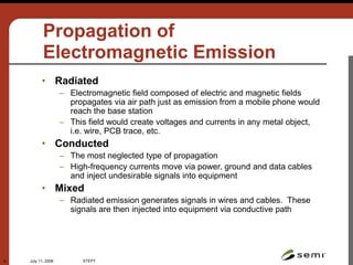
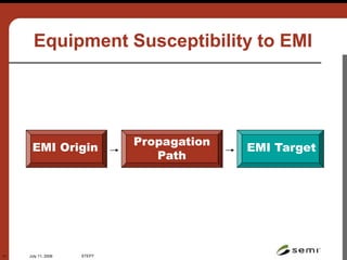
This document discusses electromagnetic compatibility (EMC) issues in semiconductor manufacturing facilities. It addresses electromagnetic interference (EMI) sources like electrostatic discharge events and mobile phones. It also covers EMI propagation through radiation, conduction, and grounding systems. Maintaining EMC requires managing EMI sources, propagation paths, and equipment susceptibility through comprehensive facility design. The SEMI E33 standard provides guidelines for equipment EMC in semiconductor fabs.


![July 11, 2006 STEP7
32
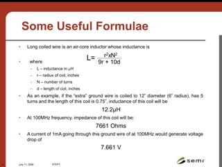
Some Useful Formulae
• Inductance of a straight wire at high frequencies can be calculated
as:
• where
– L – inductance in H
– r – radius wire, cm
– d – length of wire, cm
• A common 10m (30 feet) ground run of 12 gage solid wire has self-
inductance at high frequencies of
17.36μH
• The same 1mA current at 100MHz would create a voltage on this
length of wire of
10.9V
L=0.002d*[ln -1]
2d
r](https://image.slidesharecdn.com/krazpresentation-220928132105-f4306da4/85/Kraz_Presentation-ppt-32-320.jpg)