Download to read offline
![International Research Journal of Engineering and Technology (IRJET) e-ISSN: 2395-0056
www.irjet.net p-ISSN: 2395-0072Volume: 05 Issue: 06 | June-2018
© 2018, IRJET | Impact Factor value: 6.171 | ISO 9001:2008 Certified Journal | Page 1253
PV System Connected High Step-Up Boost DC-DC Converter Based
Voltage Compensator
K.Tamilselvan1, R.Anita2
1,2Department of Electrical and Electronics Engineering, Institute of Road and Transport Technology, Erode-
638316, Tamilnadu, India
----------------------------------------------------------------------***------------------------------------------------------------------
Abstract— In this paper, a Photovoltaic (PV) system
interfaced high step up DC-DC converter based voltage
compensator such as Dynamic Voltage Restorer (DVR) is
presented to alleviate the voltage sag and swell in low
voltage single-phase power distribution system. The PV
system supports the DC-link of the DVR. The PV array output
voltage stepped up with the use of high step up DC-DC boost
converter. The converter attains high step-up voltage gain by
means of low voltage stress on the power semiconductor
switch. Similarly, the stored energy in the coupled inductor
may be reprocessed to the load. The usage of high step up
DC-DC converter decreases the size and necessary power
rating of the series injection transformer. It as well increases
the stability and safety of the system. A feedback loop is
engaged to attain a faster response in sag/swell detection. A
single phase full bridge inverter is added to convert DC bus
voltage into a 230V, 50Hz single phase AC source by by
means of Sinusoidal Pulse Width Modulation (SPWM)
technique. Simulation results have ascertained the
proficiency of the presented PV supported DVR in alleviating
voltage sag and swell in low voltage single-phase power
distribution system.
Index Terms— Dynamic Voltage Restorer , DC-DC Boost
Converter, Photovoltaic System, Sag, Swell.
1. INTRODUCTION
DVR offers the most cost effective solution to alleviate
voltage sag and swell in the low and medium electric power
distribution system. The disturbances such as voltage sag,
swell and voltage distortion have become an accumulative
concern in both domestic and industrial customers. Voltage
sag is a sudden reduction of source voltage from 90% to
10% of its nominal value with duration from 0.5 cycles to 1
min [1].
Voltage swell is a sudden rise of supply voltage from
110% to 190% with duration from 0.5 cycles to 1 min [2,3].
This may occur in the distribution system where the grid
quality is unacceptable.
The above stated voltage variation measures happen
owing to single line to ground fault, phase to phase fault,
energization of large capacitor banks, switching of heavy
loads, starting of large motors and pressing process in steel
plants. The voltage variations events and its effects are
shown in Table 1.
Table 1
Voltage Variation Events and its Effects
Disturbances Effects
Unbalance voltage Produce excessive heat in
motor and control
equipment.
Interruption Complete shutdown.
Voltage sag Trip out the adjustable speed
drive & computer.
Voltage swell Overstress to insulation.
Fluctuations in
voltage
Light Flicker.
Harmonics Produce more noise and
overheating.
To alleviate the above stated power quality issues, the
DVR has been projected as effective sag/swell alleviation
equipment [4,5]. The injections of voltage from DVR
compensate the voltage sag/swell during sag and swell
events [6,7].
In this paper a simulation of high step up DC-DC
converter with the PV power generating system is
integrated to function as a high capacity DC voltage source.
It reduces the size and capacity of series injection
transformer. The converter practices the coupled inductor
and capacitors to attain high step up voltage gain. This
converter can offer higher voltage gain than the
conventional DC-DC boost converter [8,9].
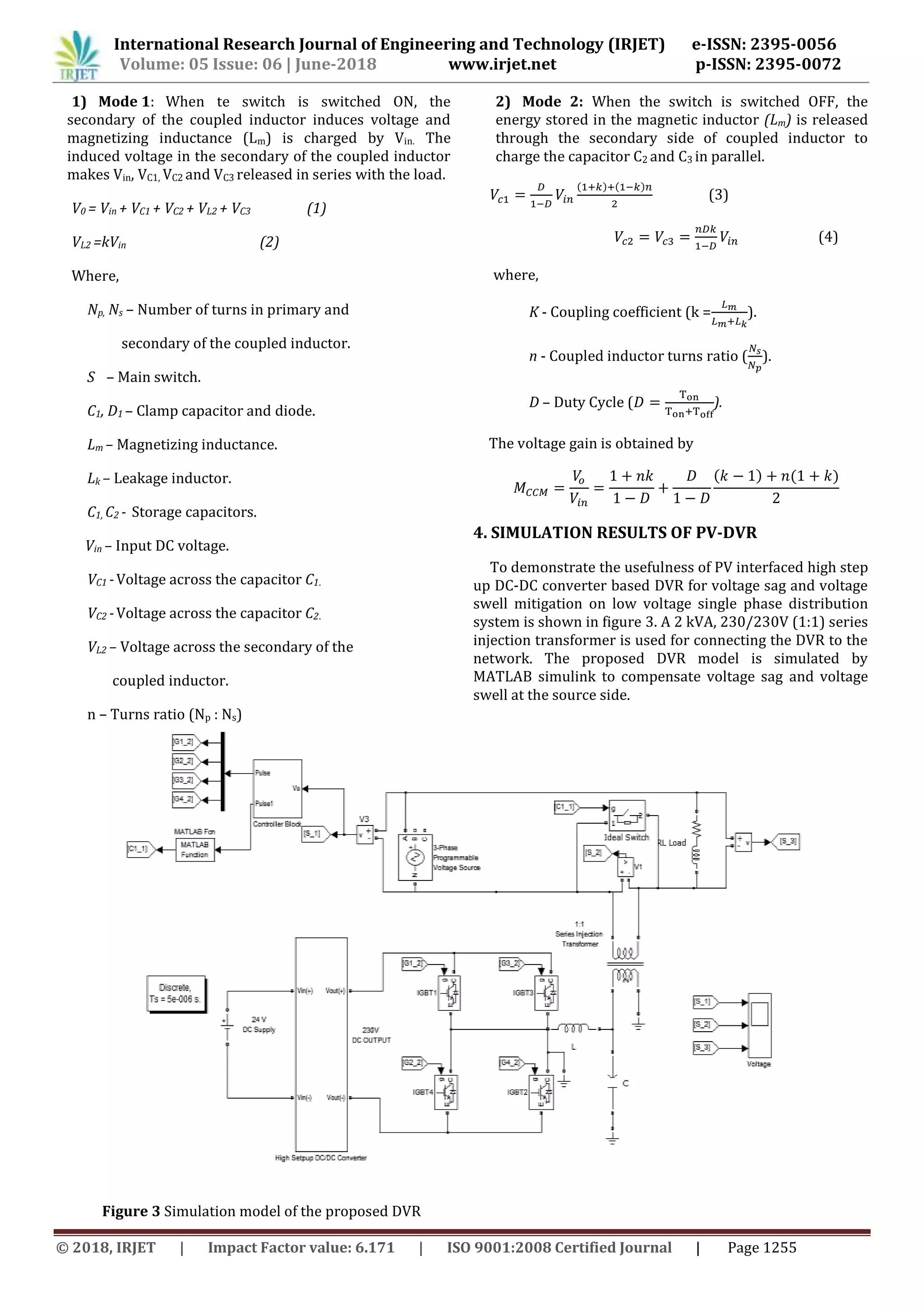
2. PV SYSTEM INTERFACED HIGH STEP UP DC-DC
CONVERTER BASED DVR
The schematic diagram of the PV supported DVR is
shown in Figure 1. The projected system includes of a
battery, high step up DC-DC converter with coupled
inductor, Voltage Source Inverter (VSI), series injection
transformer (1:1) and semiconductor bypass switch S.](https://image.slidesharecdn.com/irjet-v5i6232-180801070045/75/IRJET-PV-System-Connected-High-Step-Up-Boost-DC-DC-Converter-based-Voltage-Compensator-1-2048.jpg)
![International Research Journal of Engineering and Technology (IRJET) e-ISSN: 2395-0056
www.irjet.net p-ISSN: 2395-0072Volume: 05 Issue: 06 | June-2018
© 2018, IRJET | Impact Factor value: 6.171 | ISO 9001:2008 Certified Journal | Page 1254
Figure 1 Block diagram of the PV-DVR
Table 2 displays the control signal of semiconductor
switch S, which is connected in parallel with the secondary
of series injection transformer. The power semiconductor
switch S is controlled by voltage sensor and the simple
logical circuits.
Table 2
Control Signal of Semiconductor Switch S
Supply voltage
in %
Control
signal
Mode of
Operation
100% 1 Ideal
<100% 0 DVR
>100% 0 DVR
A DVR is connected in series with the power distribution
system to inject a compensating voltage in series with the
AC source. The main components of a DVR are the high
capacity DC source, bridge inverter, injection transformer
and control system. A DVR can compensate the voltage
drop across a sensitive load by injecting a voltage through a
series injection transformer[10,11,12].
The inverter is a foremost component of DVR. Its control
will directly distress the transient and dynamic
performance of the DVR. The voltage injection of the DVR is
mainly being subject to on the capacity of DC source, which
is connected in the DC-link of the DVR. A high step up DC-
DC converter with coupled inductor offers a high power DC
source to voltage source inverter of the DVR.
3. HIGH STEP UP DC-DC CONVERTER
A high step up DC-DC converter can boost the voltage
from low level to high level. It decreases the number of
batteries, essential to attain the mandatory DC voltage level
in that way saving the cost and space as an alternative of
using numerous batteries. In general, the DC-DC boost
converter can offer high step up voltage gain with
exceedingly high duty cycle. The step-up voltage gain is
inadequate by the effect on power semiconductor switches,
inductors and capacitors. To develop the conversion
efficiency and to achieve high step up voltage gain the
coupled inductor with switched capacitor technique is
used[9]. This converter is connected in between the low
power DC source such as renewable energy power
generation system or conventional battery storage units
and voltage source inverter. The high step up DC-DC
converter with coupled inductor is shown in Figure 2.
Figure 2 Circuit configuration of high step up DC-DC
boost converter
The secondary side (Ns) of the coupled inductor is used
as a flyback converter. It can increase the voltage gain. The
energy stored in the leakage inductor (Lk) is recycled to the
load directly. The advantages of this DC-DC converters is as
follows
It confines voltage spike on the main switch.
Delivers high step up gain.
High conversion efficiency.
Low conduction loss.
High step up ratio.
The secondary of the coupled inductor can charge
capacitors in parallel and discharge them in series with
the load. This converter combines the concept of coupled
inductor and switched capacitor techniques. The
secondary of the coupled inductor charge the capacitors
C2 and C3 when the switch is switched OFF and are
discharged in series by the secondary side of coupled
inductor when the switch is switched ON. It operates in
two mode of operation.](https://image.slidesharecdn.com/irjet-v5i6232-180801070045/75/IRJET-PV-System-Connected-High-Step-Up-Boost-DC-DC-Converter-based-Voltage-Compensator-2-2048.jpg)
![International Research Journal of Engineering and Technology (IRJET) e-ISSN: 2395-0056
www.irjet.net p-ISSN: 2395-0072Volume: 05 Issue: 06 | June-2018
© 2018, IRJET | Impact Factor value: 6.171 | ISO 9001:2008 Certified Journal | Page 1257
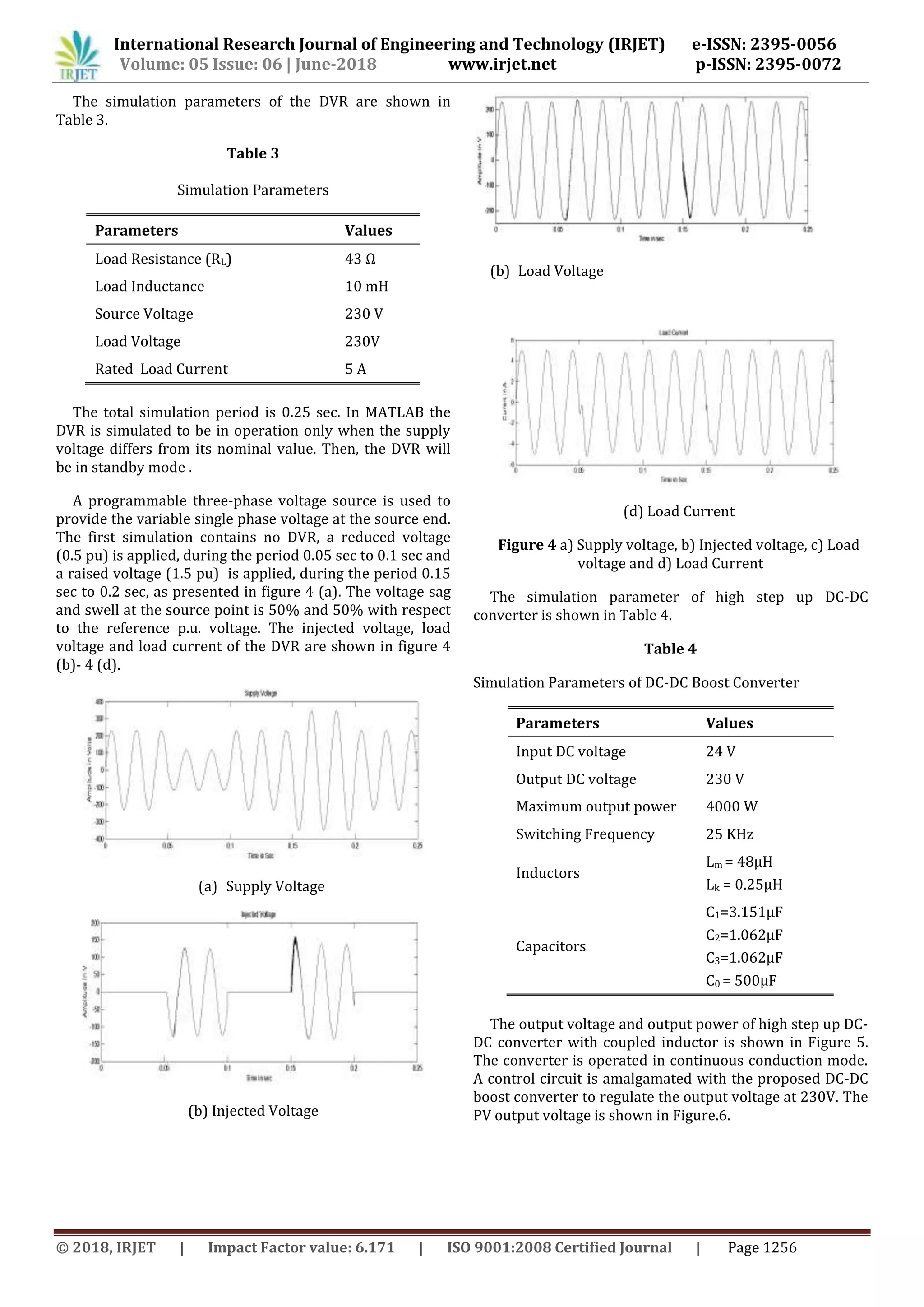
(a)
Output voltage of high step up DC-DC converter
(b) Output power of high step up DC-DC converter
Figure 5 output of High step up DC-DC converter
Figure 6 PV array output voltage
5. CONCLUSION
The PV-DVR which integrates a PV interfaced high step
up DC-DC converter as a DC voltage source to alleviate the
voltage sag and swell in a single phase low voltage electric
power distribution system has been presented. The PV
system supports the DC link of the DVR to offer long lasting
compensation against voltage based disturbances in the
power distribution system. The simulation of the proposed
system has been presented. By using the capacitor charged
in parallel and discharged in series by coupled inductor,
high step up voltage gain and high efficiency are achieved.
Furthermore, the mandatory power rating of series
injection transformer is reduced to low rating by selecting
1:1 transformer for series injection.
6. REFERENCES
[1]Amrita Rai, A.K. Nadir, “Modeling and Simulation of
Dynamic Voltage Restorer (DVR) for Enhancing Voltage
Sag,” in sensor and transducer journals, Vol. 87, issue 1, pp:
85-93, Jan 2008.
[2]F.A.L.Jowder, “Modeling and simulation of different
system topologies for dynamic voltage restorer using
simulink,” in proc. EPECS ’09, p. 1-6, Nov 2009.
[3]H.Ezoji, A.Sheikholeslami, M.Tabasi, and M.M.Saeednia,
“Simulation of dynamic voltage restorer using hysteresis
voltage control,” European journal of scientific research,
vol. 27, pp. 152-166, Feb 2009.
[4]Hyun Lark Do, “Zero voltage switching boost converter
using a coupled inductor,” Vol. 11, No. 1, pp. 16-20, Jan
2011.
[5]P.Boonchiam, and N.Mithulananthan, “Understanding of
dynamic voltage restorers through MATLAB simulation,”
Thammasat Int. J. Sc. Tech., Vol. 11, No.3, pp. 1-6, Sep 2006.
[6]R.J.Wai and R.Y.Duan, “High-efficiency DC/DC converter
with high voltage gain,” IEE Proc. Electric Power
Applications, Vol.152, No.4, pp.793-802, Jul. 2005.
[7]R.Omar, and N. Abd Rahim, “Mitigation of voltage
sags/swells using Dynamic voltage restorer (DVR),” ARPN
Journal of Engineering and Applied Sciences, Vol. 4, No. 4,
June 2009.
[8]S.K.Changchien, T.J.Liang, J.F.Chen and L.S.Yang, “Novel
high step-up DC-DC converter for fuel cell energy
conversion system,” IEEE Trans. Ind. Electronics, Vol. 57,
No.6, pp.2007-2017, June 2010.
[9]Y.P.Hsieh, J.F.Chen, T.J.Liang and L.S.Yang, “Novel high
set-up DC-DC converter for distributed generation system,”
IEEE transaction on Industrial Electronics, pp. 1-7, Jan
2011.
[10]Meyer, C., De-Doncker, R.W., Li, Y.W. and Blaabjerg, F.
“Optimized control strategy for a medium-voltage DVR-
Theoretical Investigations and experimental results”, IEEE
Transactions on Power Electronics, Vol.23, No.6, pp.2746-
2754, 2008.
[11]Mahdianpoor, F.M., Hooshmand, R.A. and Mohammad,
A. “A new approach to multifunctional dynamic voltage
restorer implementation for emergency control in
distribution systems”, IEEE Transactions on Power
Delivery, Vol.26, No.2, pp.882-890, 2011.
[12]Mohan, N., Undeland, T.M. and Robbins, W.P. “Power
Electronics Converters: Applications and Design”, Third
Edition, Jhon Wiley & Sons Asia Pte. Ltd., Singapore,
pp.172-178, 2006.](https://image.slidesharecdn.com/irjet-v5i6232-180801070045/75/IRJET-PV-System-Connected-High-Step-Up-Boost-DC-DC-Converter-based-Voltage-Compensator-5-2048.jpg)

1. The document presents a photovoltaic (PV) system interfaced with a high step-up DC-DC converter to support the DC link of a dynamic voltage restorer (DVR) and alleviate voltage sags and swells in a low voltage power distribution system. 2. The high step-up DC-DC boost converter uses a coupled inductor design to achieve high voltage gain from the low output of the PV array while maintaining low voltage stress on the power switches. This reduces the size and power rating needed for the series injection transformer. 3. Simulation results show the effectiveness of the proposed PV-supported DVR in mitigating voltage sags and swells in a low voltage single-