Download as PDF, PPTX


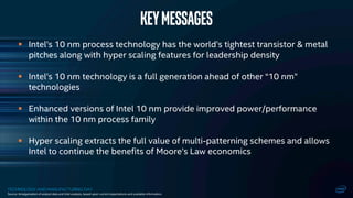


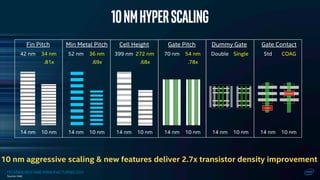
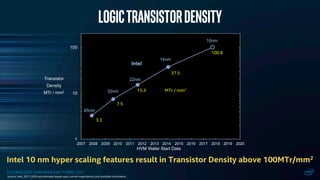
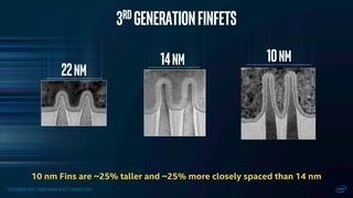
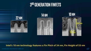
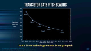

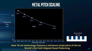
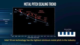

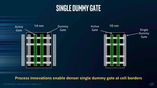


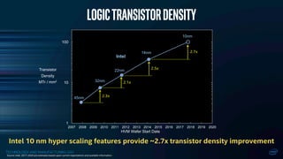
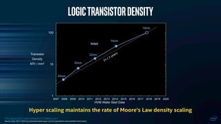
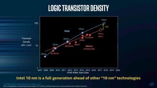


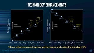
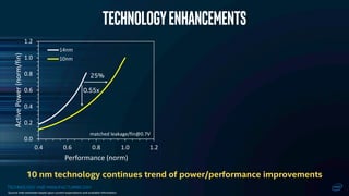
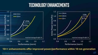
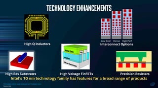


Intel's Technology and Manufacturing Day 2017 presentation highlights the advanced features and capabilities of its 10nm process technology, which offers the world's tightest transistor and metal pitches, achieving a performance advantage over competing technologies. This generation of 10nm technology includes enhancements for improved power and performance while continuing the economic benefits associated with Moore's Law through hyper scaling. Despite the quiet period before quarterly financial results, Intel presents forward-looking statements and anticipates manufacturing to begin in the second half of 2017.