Download to read offline
![http://www.iaeme.com/IJECET/index.asp 31 editor@iaeme.com
International Journal of Electronics and Communication Engineering & Technology
(IJECET)
Volume 6, Issue 7, Jul 2015, pp. 31-36, Article ID: IJECET_06_07_005
Available online at
http://www.iaeme.com/IJECETissues.asp?JTypeIJECET&VType=6&IType=7
ISSN Print: 0976-6464 and ISSN Online: 0976-6472
© IAEME Publication
___________________________________________________________________________
EXPLOITING DESIGN OF SYNCHRONOUS
COUNTERS METHOD TO DESIGN AND
IMPLEMENT MOD 6 DIRECT DOWN
COUNTER
Bawar A. Abdalla and Zhenar Sh. Faeq
Department of Software Engineering, Faculty of Engineering,
University of Koya, Koya, Iraq
Zrar Kh. Abdul
Department of General Science, University of Charmo, Chamchamal, Iraq
ABSTRACT
In this paper, the design of direct mod 6 down counter is proposed by
using J-K Flip Flop. The counter is provided with synchronous clock pulse.
The counter is implemented by using Electronic Workbench software. The
design can be achieved by the logical function minimization using Karnaugh
map. Vcc and Ground are used for inputs to indicate logic 1 and 0
respectively as well as LED indicators are used to indicate the output bits. The
proposed design is practical to implement any modulus of direct down
counters which can count from any number to zero. This can have advantage
over partial decoding method to design counters which their modulus does not
belong to 2n
sequence because partial decoding method is only practical for
up counters.
Key words: Down Counter, Mod 6 Down Counter and Synchronous
Counters.
Cite this Article: Abdalla, B. A., Faeq, Z. S. and Abdul, Z. K. Exploiting
Design of Synchronous Counters Method to Design and Implement Mod 6
Direct Down Counter. International Journal of Electronics and
Communication Engineering & Technology, 6(7), 2015, pp. 31-36.
http://www.iaeme.com/IJECET/issues.asp?JTypeIJECET&VType=6&IType=7
_____________________________________________________________________
1. INTRODUCTION
Counting is a fundamental function of digital circuits [1]. It can be performed by
counters which are named as sequential circuits that change their states by the clock](https://image.slidesharecdn.com/ijecet0607005-150820075233-lva1-app6891/75/Ijecet-06-07_005-1-2048.jpg)
![Bawar A. Abdalla, Zhenar Sh. Faeq and Zrar Kh. Abdul
http://www.iaeme.com/IJECET/index.asp 32 editor@iaeme.com
pulses applied on their inputs. They can be used in real world applications ranging
from a simple display to complex microcontroller circuits. Some of the applications
are digital systems, with applications in computer systems, communication
equipment, scientific instruments, and industrial control [2]. Obviously, the counters’
primary function is producing a sequence of different output patterns. Hence, they
also can be named as pattern generators. These sequence of pattern scan be assigned
to a number of an event’s occurrences as well as it can be used to control and select
each specific part of a digital system. In this way each output state of pattern indicates
the performance of each distinct part of the digital system [3]. Basically, a counter is a
logic circuit that counts up to a specific number. Each count is a binary number as
well as called the state of the counter. Moreover, the number of states of a counter is
called modulus of the counter and can be determined by the number of bits used to
design the counter. Thus, an n bit counter has 2n
states and called as module 2n
counter where n is an integer number [2].
It is clear that essential elements that associated in designing the semiconductor
devices are Flip Flops [4]. There are many types of Flip Flops such as SR, D, T and
JK. They can be connected together to perform the function of a counter. This means
a group of Flip Flops is a counter, the number of states and the modulus of the counter
can be determined through the number of Flip Flops whereas each Flip Flop holds one
binary bit in the output pattern of the counter. In addition, according to the connection
design of the Flip Flops together and the way the counter circuits are clocked, the
Counters can be categorized in to two main categories which are asynchronous and
synchronous. In asynchronous counters each Flip Flop receives clock pulse from the
previous Flip Flop while in the synchronous counters all the Flip Flops are receiving
their clock pulses simultaneously [5].
2. BACKGROUND
2.1 J-K Flip-Flop
J-K Flip-flop is like the other Flip Flops while the outputs are affected by the inputs
when the Clock is high for positive edges and low for negative edges, also there are
two inputs associated with this type of Flip Flop which are labeled as J and K.
Furthermore, if both J and K are low and the clock pulse is applied, the output will not
change as it stays as the same as the previous output state. If both J and K are high,
the output will toggle from the previous output state. Finally, if J and K are different
and the clock is applied the output state will follow the J input [10, 11]. The
advantage of J-K Flip Flop is that it does not have any invalid state as occurred in S-R
Flip Flop while both S and R are high [8]. Table 1 shows the truth table of J-K Flip
Flop.
Table 1 J-K Flip Flop Truth table
Moreover, the J-K Flip Flop Transition table can be seen from Table 2.](https://image.slidesharecdn.com/ijecet0607005-150820075233-lva1-app6891/75/Ijecet-06-07_005-2-2048.jpg)
![Exploiting Design of Synchronous Counters Method to Design and Implement Mod 6 Direct
Down Counter
http://www.iaeme.com/IJECET/index.asp 33 editor@iaeme.com
Table 2 J-K Flip Flop Transition table
2.2. Counter Modulus
Counters can perform up counting to a maximum state according to the number of
Flip Flops. For example, 2 bits counter has 22
states which can count from zero to
three. This is called up counter. However, down counter produces a sequence from the
maximum state to zero. For example, 3 bits counter can produce a sequence from
seven to zero. In some applications, it is required that the counter should perform both
up and down counting which is called up/down counter [6]. According to number of
Flip Flops in the counters, the modulus of the counters is 2,4,8,16,32 and etc. This is
because of that the number of states is 2n
where n is the number of Flip Flops.
However, some applications might need a modulus which is not in the 2n
sequence
such as modulus 4, 6, 7 and 9. In this case, there should be a mechanism to reset the
counter after the maximum required state such as modulus 6 counts from 0 to 5 and
should be cleared at the state of 6. This mechanism is called partial decoding [5]. In
addition, this mechanism is only practical for up counters while it doesn’t work for
down counters. The aim of this paper is to exploit synchronous counter design to
implement a practical high performance synchronous down counter which its modulus
doesn’t belong to the 2n
sequences such as modulus 6 down counter as a case study by
using Electronic Workbench Software.
In this paper, Electronics Workbench (EWB) has been used to design and simulate
the circuit since it is friendly as well as it provides an interface as close as to the real
implementation environment [7]. It provides TTL logic levels (+Vcc) used to indicate
logic high for the inputs. It also provides an output circuit which is called “indicator
lamp” to represent the output state of a single bit, it indicates logic high in case when
it turns on, and else it indicates logic 0 [9].
3. DESIGNING AND TESTING THE MOD 6 DOWN COUNTER
To start with, synchronous counters need some special mathematical calculations.
This can be done by drawing the counter state diagram as can be seen from Figure 1.
Figure 1 Counter state diagram
After that, the table of the counter’s logical function can be built as it is shown in
table (3). This can be done by listing each present state of the counter with the
corresponding next state [5].
Q N Q N+1 J K
0 0 0 X
0 1 1 X
1 1 X 0
1 0 X 1](https://image.slidesharecdn.com/ijecet0607005-150820075233-lva1-app6891/75/Ijecet-06-07_005-3-2048.jpg)
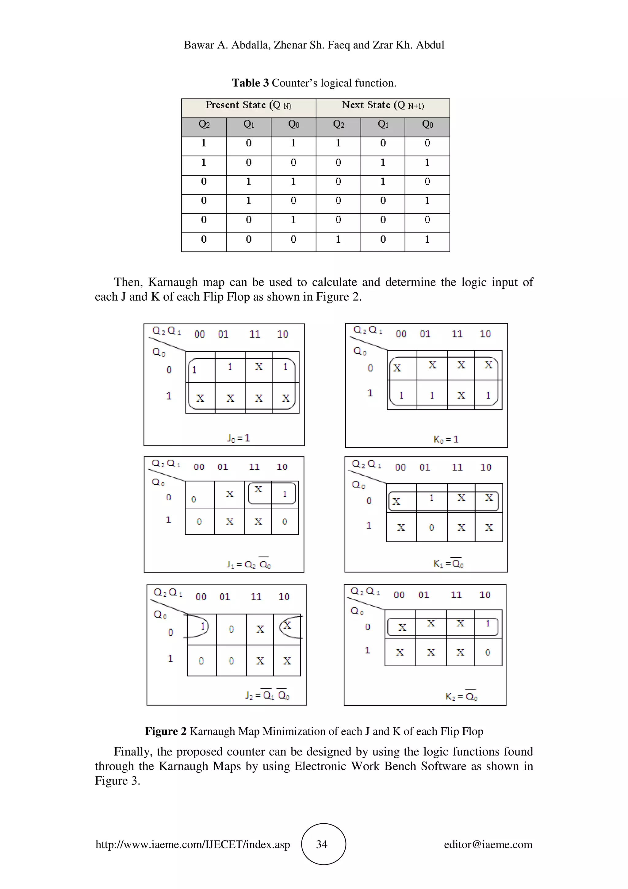
![Bawar A. Abdalla, Zhenar Sh. Faeq and Zrar Kh. Abdul
http://www.iaeme.com/IJECET/index.asp 36 editor@iaeme.com
4. CONCLUSION
In conclusion, J-K Flip Flops were used to design the synchronous mod 6 down
counter. The input of each J and K of the Flip Flops can be determined through the
counter’s logical function and Karnaugh map. The proposed counter was designed
and implemented by using electronic workbench software which is sufficient for
designing purposes. The counter could count from 5 to 0 by applying synchronous
clock pulses to the negative edges of each Flip Flop. It can be suggested that the
exploited method to design the counter is practical to design any modulus of direct
down counters as well as for up counters.
REFERENCES
[1] Yogita, H., Akalpita, K. L. and Baligar, J. S. Design and Implementation of
Synchronous 4-bitup Counter Using 180NM CMOS Process Technology.
International Journal of Research in Engineering and Technology. 3(5), 2014.
[2] Matey, C. V., Mendhe, S. K. and Zade, S. A. A Novel Design of Counter Using
TSPC D FLIP-FLOP for High Performance and Low Power VLSI Design
Applications Using 45NM CMOS Technology. International Journal of Science
Technology & Management, 4(Special Issue 01), 2015.
[3] Givone, D. D. Digital Principles and Design, McGraw-Hill, 2003.
[4] Tschanz, J., Narendra, S., Chen, Z., Borkar, S., Sachdev, M. and De, V.
Comparative delay and energy of single edge triggered and dual edgetriggered
pulsed flip-flops for high performance microprocessors. In Proc. ISPLED, 2001,
pp. 207–212.
[5] Floyd, T. L. Digital Fundamentals, Fourth Edition. Macmillan Publishing, 1990,
p. 395.
[6] Hawrra, R. H. Implementation Modified Counters using Fredkin & Feynman
Logic Gates. Journal of Kerbala University, 6(3), 2008.
[7] Aissi, C. and Kazakos, D. A review of chaotic circuits, simulation and
implementation. In Proceedings of the 10th WSEAS international conference on
Circuits2006, World Scientific and Engineering Academy and Society (WSEAS),
Athens, Greece. pp. 125–131.
[8] Bhaskar, M. V., Sukhavasi, S. B., Sukhavasi, S. B. and Vemana, G. S. S.
Implementation of Synchronous UP Counterby Using Self Resetting Logic.
International Journal of Engineering Research and Applications. 2(1), 2012.
[9] Drăghici, S. and Drugărin, C. V. A. The Design of the Moebius Mod-6 Counter
Using Electronic Workbench Software. Procedia Social and Behavioral Sciences,
191, 2015, pp. 2316–2324.
[10] Dai, Y. and Shen, J. An explicit-pulsed double edge triggered JK flip flop. IEEE
Conference Publication, 2009, pp. 1–4.
[11] Varun, I. and Gupta, T. K. Ultra-low power NAND based multiplexer and flip
flop. IEEE International Conference, 2013, pp. 1–5.](https://image.slidesharecdn.com/ijecet0607005-150820075233-lva1-app6891/75/Ijecet-06-07_005-6-2048.jpg)

1. The document describes the design and implementation of a mod 6 direct down counter using J-K flip flops and the synchronous counters method. 2. The design exploits Karnaugh maps to determine the logic inputs for each J-K flip flop in order to minimize the logic functions. 3. The mod 6 down counter is implemented using Electronic Workbench software with 3 J-K flip flops that count synchronously from 5 to 0 on each clock pulse before repeating the cycle.


![COUNTERS [Synchronous and Asynchronous]](https://cdn.slidesharecdn.com/ss_thumbnails/counters-211217083059-thumbnail.jpg?width=640&height=640&fit=bounds)