Half Wave Controlled Rectifier with Resistive Load.pptx
1.
1
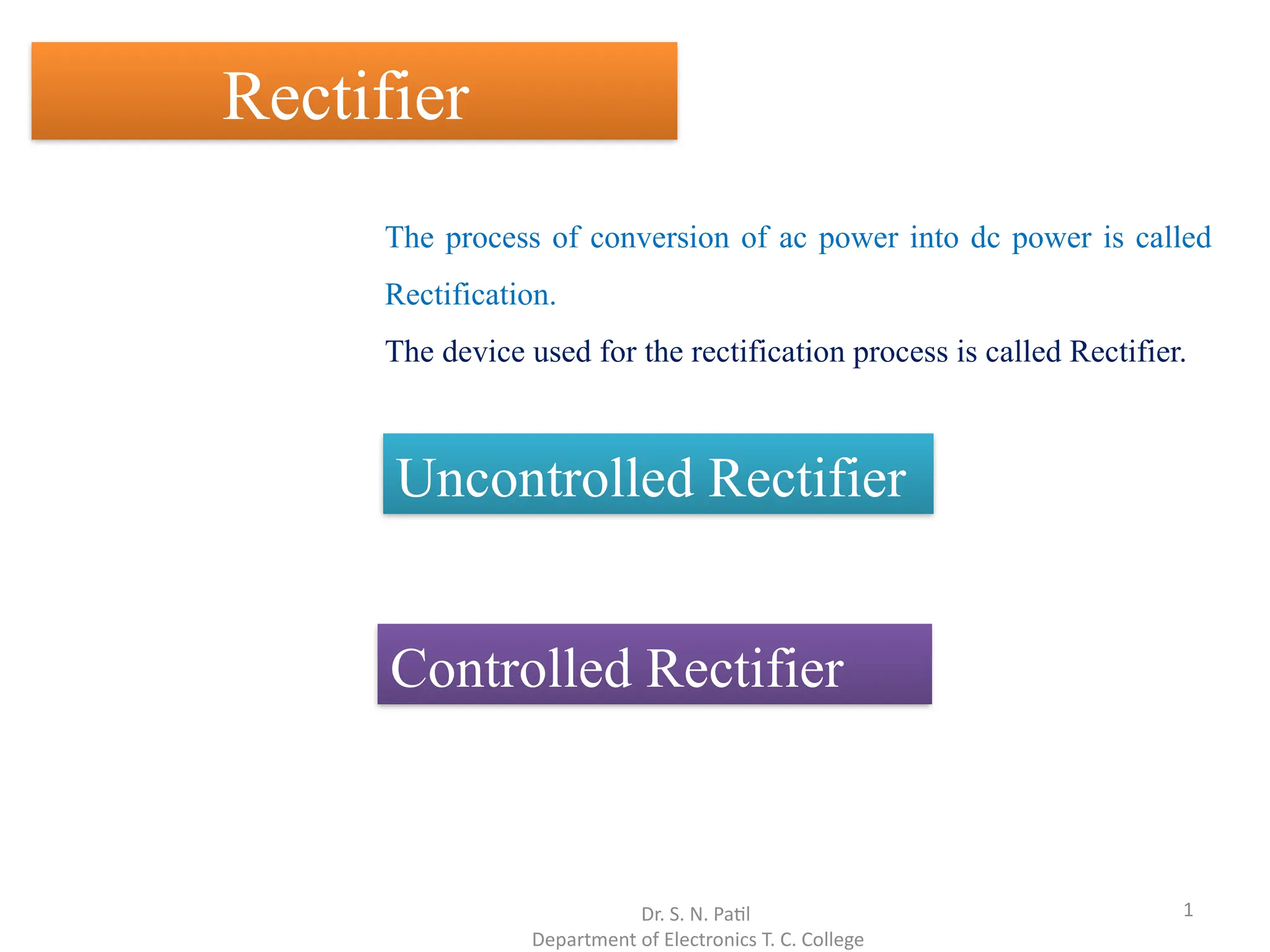
Rectifier
Controlled Rectifier
Uncontrolled Rectifier
Dr.S. N. Patil
Department of Electronics T. C. College
The process of conversion of ac power into dc power is called
Rectification.
The device used for the rectification process is called Rectifier.
2.
2
The controlled rectifierscan be single-phase or three-phase. Based on
control over output voltage, there are two types of controlled rectifiers,
Dr. S. N. Patil
Department of Electronics T. C. College
In normal rectifiers, which includes P-N junction semiconductor diodes, the output
voltage obtained is fixed in amplitude by the amplitude of ac input voltage.
So in order to obtain controllable variable dc output, controlled rectifiers are
used.
Controlled rectifiers incorporate phase-controlled thyristors instead of diodes to
obtain the variable output.
3.
3
Half Wave ControlledRectifier and,
Full Wave Controlled Rectifier.
In this article, let us learn about half-wave controlled rectifiers.
In practice, the performance of controlled rectifiers gets affected by
the type of load (Resistive, Inductive, or Capacitive) to which it is
supplying power.
So, let us see the operation of half-wave controlled rectifiers with
various types of loads.
Dr. S. N. Patil
Department of Electronics T. C. College
4.
4
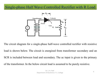
The circuit diagramfor a single-phase half-wave controlled rectifier with resistive
load is shown below. The circuit is energized from transformer secondary and an
SCR is included between load and secondary. The ac input is given to the primary
of the transformer. In the below circuit load is assumed to be purely resistive.
Dr. S. N. Patil
Department of Electronics T. C. College
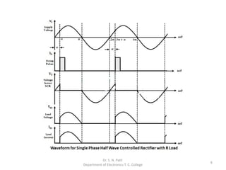
Single-phase Half Wave Controlled Rectifier with R Load
Anode
Cathode
Gate
5.
5
Working of Single-phaseHalf Wave Controlled Rectifier with R Load :
During the negative half cycle of supply voltage, the SCR is reverse-biased, so there will be no
conduction even if the gate is triggered. Hence, the entire supply voltage appears across SCR. The
waveforms for the above circuit operation with resistive load are illustrated below.
Dr. S. N. Patil
Department of Electronics T. C. College
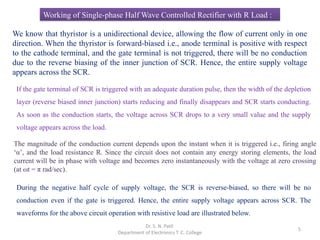
We know that thyristor is a unidirectional device, allowing the flow of current only in one
direction. When the thyristor is forward-biased i.e., anode terminal is positive with respect
to the cathode terminal, and the gate terminal is not triggered, there will be no conduction
due to the reverse biasing of the inner junction of SCR. Hence, the entire supply voltage
appears across the SCR.
If the gate terminal of SCR is triggered with an adequate duration pulse, then the width of the depletion
layer (reverse biased inner junction) starts reducing and finally disappears and SCR starts conducting.
As soon as the conduction starts, the voltage across SCR drops to a very small value and the supply
voltage appears across the load.
The magnitude of the conduction current depends upon the instant when it is triggered i.e., firing angle
‘α’, and the load resistance R. Since the circuit does not contain any energy storing elements, the load
current will be in phase with voltage and becomes zero instantaneously with the voltage at zero crossing
(at ωt = π rad/sec).
6.
6
Dr. S. N.Patil
Department of Electronics T. C. College
7.
7
In the abovewaveforms, the load current and voltage are zero from 0 to α.
When SCR is triggered by giving gate signal at α. The entire supply voltage
except for drop across SCR will be applied across the load (from ωt = α to ωt
= π). At ωt = π, the phase reversal takes place and the negative half-cycle of
the input supply will start.
Due to the negative half-cycle, the SCR will be reverse biased and will be
turned OFF at ωt = π. From ωt = π to ωt = 2π, the load current and voltage
will be zero. That is SCR is naturally commuted.
Again when the positive half cycle starts i.e., from ωt = 2π, SCR will be
forward biased but it will not be switched ON until it is triggered
i.e. until ωt = (2π + α).
Dr. S. N. Patil
Department of Electronics T. C. College
8.
Dr. S. N.Patil Department of Electronics T. C
. College
8
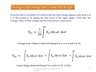
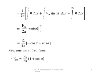
From the above waveform, It is shown that the load voltage appears only from α to
π in the period of 2π during the first cycle of the input supply. From this, the
average value of load voltage and the load current is derived as,
Average Load Voltage and Current with R load :
Average load voltage is observed during 0 to α, α to π and π to 2π
Load voltage observed during 0 to α and π to 2π is Zero
9.
Dr. S. N.Patil Department of Electronics T. C
. College
9
10.
Dr. S. N.Patil Department of Electronics T. C
. College
10
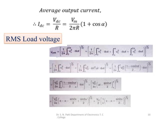
RMS Load voltage
11.
Dr. S. N.Patil Department of Electronics T. C
. College
11
Therefore, from the above equation, the average output
voltage across the load can be varied by varying the firing
angle α. The maximum output voltage across the load is
obtained when firing angle α = 0.
12.
Dr. S. N.Patil Department of Electronics T. C
. College
12
THANK YOU!!