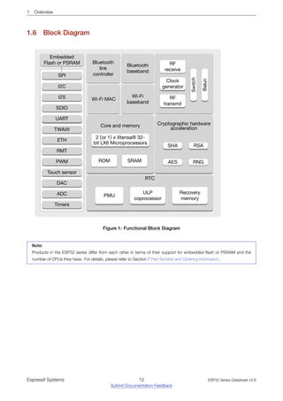
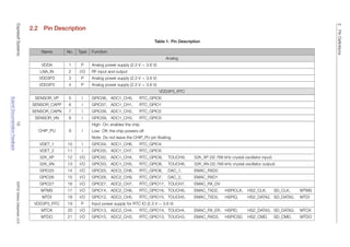
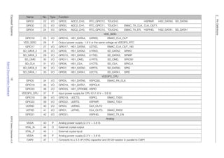
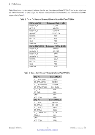
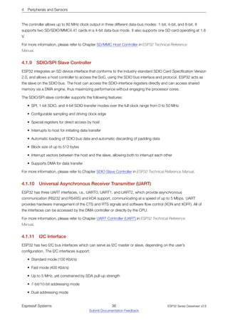
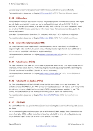
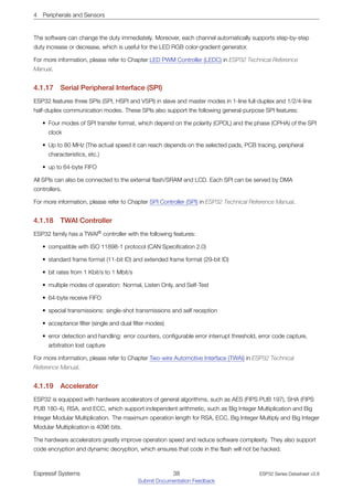
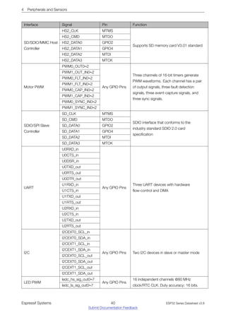
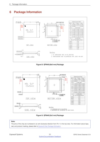
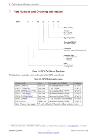
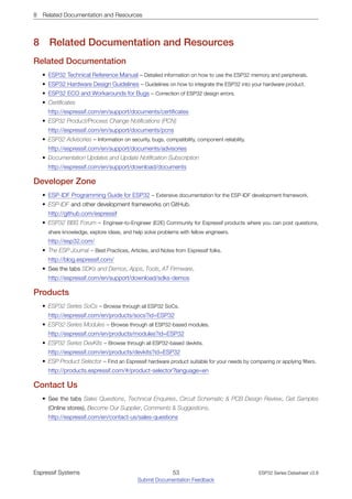
This document provides specifications for the ESP32 series of Wi-Fi and Bluetooth combo chips. It includes information on the chip's features such as its CPU, memory, radio capabilities, peripherals, and electrical characteristics. The document also includes pin definitions, package information, part numbers, and documentation resources.
4 Channel Relay Board 5V-Bluetooth Compatible for ArduinoRaghav Shetty
Bluetooth technology is a short distance communication technology used by almost all phones
including smart phones and all laptops. This technology find very wide uses including that of Home &
Industrial automation.
The Relay shield is capable of controlling 4 relays. The max switching power could be
12A/250VAC or 15A/24VDC. It could be directly controlled by Arduino through digital IOs.
Webinar: BlueNRG-LP - Bluetooth 5.2 de longo alcance para aplicações industriaisEmbarcados
O BlueNRG-LP é uma solução de SoC sem fio Bluetooth® Low Energy programável de ultrabaixa energia. Ele incorpora os IPs de rádio RF de 2,4 GHz de última geração da STMicroelectronics combinando desempenho incomparável com vida útil de bateria extremamente longa. É compatível com a especificação de núcleo Bluetooth® Low Energy SIG versão 5.2 endereçando conectividade ponto a ponto e rede Bluetooth Mesh e permite que redes de dispositivos em grande escala sejam estabelecidas de maneira confiável. O BlueNRG-LP também é adequado para comunicação sem fio de rádio proprietária de 2,4 GHz para lidar com aplicações de latência ultrabaixa.
Assista a gravação em: https://www.embarcados.com.br/webinars/webinar-bluenrg-lp-bluetooth-5-2-de-longo-alcance-para-aplicacoes-industriais/
The MC13202 is the 2nd generation 2.4 GHz band transceiver designed for?wireless sensing and control applications.? The MC13202 includes a complete packet modem capable of formatting data into packets with 125 byte payload. It has an over the air data rate of 250 kbps using O-QPSK modulation and Direct Sequence Spread Spectrum (DSSS) coding.? It builds on the first generation product by integrating a Transmit/receive switch that lowers the overall component count, size and cost of the solution. The four wire serial peripheral interface (SPI) allows interface to a variety of processors, providing developers to tailor the solution to meet their needs.? NXP? offers a variety of MCU that range from 8 to 32bit that easily connect to the MC13202.? The software and processor can be scaled to fit applications ranging from simple point-to-point systems, through complete ZigBee? networking.? The 13202 supports the SMAC software, IEEE 802.15.4 PHY/MAC and 3rd party ZigBee stacks.
Microcontrolador STM32WL55 - Fazendo uma aplicação LORAWAN do zero em poucos ...Embarcados
Neste evento teremos a oportunidade de fazer uma aplicação LoRaWAN do zero, através do nosso IDE, fazendo todo o processo de seleção dos periféricos, configuração de I/Os, Modo Low Power,etc. Também conectar a Rede LoRa da American Tower e finalmente fazendo o controle das regras da aplicação pelo painel WEB da TAGO.
Mais detalhes em: https://www.embarcados.com.br/evento-online-microcontrolador-stm32wl55/
HI-3220 ARINC 429 DATA MANAGEMENT ENGINE
16 x RECEIVERS, 8 x TRANSMITTERS, ADK-3220. Application Development Kit Users Guide and High Density 16Rx / 8Tx or 8Rx / 4Tx ARINC 429 HI-3220 datasheet.
Wireless energy meter monitoring with automated tariff calculationUdayalakshmi JK
Electricity billing has become a difficult task. The board has to make regular visit to the consumers house to make the reading. Also it can cause manual error. Now here we are monitoring the energy meter with modern techniques. The total energy consumed by the consumer and the consumption cost is known to the consumer and to the board by means of a hand held device.
Final project report on grocery store management system..pdfKamal Acharya
In today’s fast-changing business environment, it’s extremely important to be able to respond to client needs in the most effective and timely manner. If your customers wish to see your business online and have instant access to your products or services.
Online Grocery Store is an e-commerce website, which retails various grocery products. This project allows viewing various products available enables registered users to purchase desired products instantly using Paytm, UPI payment processor (Instant Pay) and also can place order by using Cash on Delivery (Pay Later) option. This project provides an easy access to Administrators and Managers to view orders placed using Pay Later and Instant Pay options.
In order to develop an e-commerce website, a number of Technologies must be studied and understood. These include multi-tiered architecture, server and client-side scripting techniques, implementation technologies, programming language (such as PHP, HTML, CSS, JavaScript) and MySQL relational databases. This is a project with the objective to develop a basic website where a consumer is provided with a shopping cart website and also to know about the technologies used to develop such a website.
This document will discuss each of the underlying technologies to create and implement an e- commerce website.
Water scarcity is the lack of fresh water resources to meet the standard water demand. There are two type of water scarcity. One is physical. The other is economic water scarcity.
Overview of the fundamental roles in Hydropower generation and the components involved in wider Electrical Engineering.
This paper presents the design and construction of hydroelectric dams from the hydrologist’s survey of the valley before construction, all aspects and involved disciplines, fluid dynamics, structural engineering, generation and mains frequency regulation to the very transmission of power through the network in the United Kingdom.
Author: Robbie Edward Sayers
Collaborators and co editors: Charlie Sims and Connor Healey.
(C) 2024 Robbie E. Sayers
Industrial Training at Shahjalal Fertilizer Company Limited (SFCL)MdTanvirMahtab2
This presentation is about the working procedure of Shahjalal Fertilizer Company Limited (SFCL). A Govt. owned Company of Bangladesh Chemical Industries Corporation under Ministry of Industries.
Immunizing Image Classifiers Against Localized Adversary Attacksgerogepatton
This paper addresses the vulnerability of deep learning models, particularly convolutional neural networks
(CNN)s, to adversarial attacks and presents a proactive training technique designed to counter them. We
introduce a novel volumization algorithm, which transforms 2D images into 3D volumetric representations.
When combined with 3D convolution and deep curriculum learning optimization (CLO), itsignificantly improves
the immunity of models against localized universal attacks by up to 40%. We evaluate our proposed approach
using contemporary CNN architectures and the modified Canadian Institute for Advanced Research (CIFAR-10
and CIFAR-100) and ImageNet Large Scale Visual Recognition Challenge (ILSVRC12) datasets, showcasing
accuracy improvements over previous techniques. The results indicate that the combination of the volumetric
input and curriculum learning holds significant promise for mitigating adversarial attacks without necessitating
adversary training.
About
Indigenized remote control interface card suitable for MAFI system CCR equipment. Compatible for IDM8000 CCR. Backplane mounted serial and TCP/Ethernet communication module for CCR remote access. IDM 8000 CCR remote control on serial and TCP protocol.
• Remote control: Parallel or serial interface.
• Compatible with MAFI CCR system.
• Compatible with IDM8000 CCR.
• Compatible with Backplane mount serial communication.
• Compatible with commercial and Defence aviation CCR system.
• Remote control system for accessing CCR and allied system over serial or TCP.
• Indigenized local Support/presence in India.
• Easy in configuration using DIP switches.
Technical Specifications
Indigenized remote control interface card suitable for MAFI system CCR equipment. Compatible for IDM8000 CCR. Backplane mounted serial and TCP/Ethernet communication module for CCR remote access. IDM 8000 CCR remote control on serial and TCP protocol.
Key Features
Indigenized remote control interface card suitable for MAFI system CCR equipment. Compatible for IDM8000 CCR. Backplane mounted serial and TCP/Ethernet communication module for CCR remote access. IDM 8000 CCR remote control on serial and TCP protocol.
• Remote control: Parallel or serial interface
• Compatible with MAFI CCR system
• Copatiable with IDM8000 CCR
• Compatible with Backplane mount serial communication.
• Compatible with commercial and Defence aviation CCR system.
• Remote control system for accessing CCR and allied system over serial or TCP.
• Indigenized local Support/presence in India.
Application
• Remote control: Parallel or serial interface.
• Compatible with MAFI CCR system.
• Compatible with IDM8000 CCR.
• Compatible with Backplane mount serial communication.
• Compatible with commercial and Defence aviation CCR system.
• Remote control system for accessing CCR and allied system over serial or TCP.
• Indigenized local Support/presence in India.
• Easy in configuration using DIP switches.
Explore the innovative world of trenchless pipe repair with our comprehensive guide, "The Benefits and Techniques of Trenchless Pipe Repair." This document delves into the modern methods of repairing underground pipes without the need for extensive excavation, highlighting the numerous advantages and the latest techniques used in the industry.
Learn about the cost savings, reduced environmental impact, and minimal disruption associated with trenchless technology. Discover detailed explanations of popular techniques such as pipe bursting, cured-in-place pipe (CIPP) lining, and directional drilling. Understand how these methods can be applied to various types of infrastructure, from residential plumbing to large-scale municipal systems.
Ideal for homeowners, contractors, engineers, and anyone interested in modern plumbing solutions, this guide provides valuable insights into why trenchless pipe repair is becoming the preferred choice for pipe rehabilitation. Stay informed about the latest advancements and best practices in the field.
Saudi Arabia stands as a titan in the global energy landscape, renowned for its abundant oil and gas resources. It's the largest exporter of petroleum and holds some of the world's most significant reserves. Let's delve into the top 10 oil and gas projects shaping Saudi Arabia's energy future in 2024.
2. About This Document
This document provides the specifications of ESP32 series of chips.
Document Updates
Please always refer to the latest version on https://www.espressif.com/en/support/download/documents.
Revision History
For any changes to this document over time, please refer to the last page.
Documentation Change Notification
Espressif provides email notifications to keep customers updated on changes to technical documentation.
Please subscribe at www.espressif.com/en/subscribe. Note that you need to update your subscription to receive
notifications of new products you are not currently subscribed to.
Certification
Download certificates for Espressif products from www.espressif.com/en/certificates.
3. Contents
Contents
1 Overview 8
1.1 Featured Solutions 8
1.1.1 Ultra-Low-Power Solution 8
1.1.2 Complete Integration Solution 8
1.2 Wi-Fi Key Features 8
1.3 Bluetooth Key Features 9
1.4 MCU and Advanced Features 9
1.4.1 CPU and Memory 9
1.4.2 Clocks and Timers 10
1.4.3 Advanced Peripheral Interfaces 10
1.4.4 Security 10
1.5 Applications (A Non-exhaustive List) 11
1.6 Block Diagram 12
2 Pin Definitions 13
2.1 Pin Layout 13
2.2 Pin Description 15
2.3 Power Scheme 19
2.4 Strapping Pins 21
3 Functional Description 23
3.1 CPU and Memory 23
3.1.1 CPU 23
3.1.2 Internal Memory 23
3.1.3 External Flash and SRAM 24
3.1.4 Memory Map 24
3.2 Timers and Watchdogs 26
3.2.1 64-bit Timers 26
3.2.2 Watchdog Timers 26
3.3 System Clocks 27
3.3.1 CPU Clock 27
3.3.2 RTC Clock 27
3.3.3 Audio PLL Clock 27
3.4 Radio 27
3.4.1 2.4 GHz Receiver 28
3.4.2 2.4 GHz Transmitter 28
3.4.3 Clock Generator 28
3.5 Wi-Fi 28
3.5.1 Wi-Fi Radio and Baseband 29
3.5.2 Wi-Fi MAC 29
3.6 Bluetooth 29
3.6.1 Bluetooth Radio and Baseband 29
Espressif Systems 3
Submit Documentation Feedback
ESP32 Series Datasheet v3.8
4. Contents
3.6.2 Bluetooth Interface 30
3.6.3 Bluetooth Stack 30
3.6.4 Bluetooth Link Controller 30
3.7 RTC and Low-Power Management 31
4 Peripherals and Sensors 33
4.1 Descriptions of Peripherals and Sensors 33
4.1.1 General Purpose Input/Output Interface (GPIO) 33
4.1.2 Analog-to-Digital Converter (ADC) 33
4.1.3 Hall Sensor 34
4.1.4 Digital-to-Analog Converter (DAC) 34
4.1.5 Touch Sensor 34
4.1.6 Ultra-Low-Power (ULP) Coprocessor 35
4.1.7 Ethernet MAC Interface 35
4.1.8 SD/SDIO/MMC Host Controller 35
4.1.9 SDIO/SPI Slave Controller 36
4.1.10 Universal Asynchronous Receiver Transmitter (UART) 36
4.1.11 I2C Interface 36
4.1.12 I2S Interface 37
4.1.13 Infrared Remote Controller (RMT) 37
4.1.14 Pulse Counter (PCNT) 37
4.1.15 Pulse Width Modulation (PWM) 37
4.1.16 LED PWM 37
4.1.17 Serial Peripheral Interface (SPI) 38
4.1.18 TWAI Controller 38
4.1.19 Accelerator 38
4.2 Peripheral Pin Configurations 39
5 Electrical Characteristics 44
5.1 Absolute Maximum Ratings 44
5.2 Recommended Operating Conditions 44
5.3 DC Characteristics (3.3 V, 25 °C) 45
5.4 Reliability Qualifications 45
5.5 RF Power-Consumption Specifications 46
5.6 Wi-Fi Radio 46
5.7 Bluetooth Radio 47
5.7.1 Receiver – Basic Data Rate 47
5.7.2 Transmitter – Basic Data Rate 47
5.7.3 Receiver – Enhanced Data Rate 48
5.7.4 Transmitter – Enhanced Data Rate 48
5.8 Bluetooth LE Radio 49
5.8.1 Receiver 49
5.8.2 Transmitter 50
6 Package Information 51
Espressif Systems 4
Submit Documentation Feedback
ESP32 Series Datasheet v3.8
5. Contents
7 Part Number and Ordering Information 52
8 Related Documentation and Resources 53
Appendix A – ESP32 Pin Lists 54
A.1. Notes on ESP32 Pin Lists 54
A.2. GPIO_Matrix 56
A.3. Ethernet_MAC 61
A.4. IO_MUX 61
Revision History 63
Espressif Systems 5
Submit Documentation Feedback
ESP32 Series Datasheet v3.8
6. List of Tables
List of Tables
1 Pin Description 15
2 Pin-to-Pin Mapping Between Chip and Embedded Flash/PSRAM 18
3 Connection Between Chip and External Flash/PSRAM 18
4 Description of ESP32 Power-up and Reset Timing Parameters 20
5 Strapping Pins 21
6 Parameter Descriptions of Setup and Hold Times for the Strapping Pins 22
7 Memory and Peripheral Mapping 25
8 Power Consumption by Power Modes 31
9 ADC Characteristics 33
10 ADC Calibration Results 34
11 Capacitive-Sensing GPIOs Available on ESP32 34
12 Peripheral Pin Configurations 39
13 Absolute Maximum Ratings 44
14 Recommended Operating Conditions 44
15 DC Characteristics (3.3 V, 25 °C) 45
16 Reliability Qualifications 45
17 RF Power-Consumption Specifications 46
18 Wi-Fi Radio Characteristics 46
19 Receiver Characteristics – Basic Data Rate 47
20 Transmitter Characteristics – Basic Data Rate 47
21 Receiver Characteristics – Enhanced Data Rate 48
22 Transmitter Characteristics – Enhanced Data Rate 49
23 Receiver Characteristics – Bluetooth LE 49
24 Transmitter Characteristics – Bluetooth LE 50
25 ESP32 Ordering Information 52
26 Notes on ESP32 Pin Lists 54
27 GPIO_Matrix 56
28 Ethernet_MAC 61
Espressif Systems 6
Submit Documentation Feedback
ESP32 Series Datasheet v3.8
7. List of Figures
List of Figures
1 Functional Block Diagram 12
2 ESP32 Pin Layout (QFN 6*6, Top View) 13
3 ESP32 Pin Layout (QFN 5*5, Top View) 14
4 ESP32 Power Scheme 19
5 ESP32 Power-up and Reset Timing 20
6 Setup and Hold Times for the Strapping Pins 22
7 Address Mapping Structure 24
8 QFN48 (6x6 mm) Package 51
9 QFN48 (5x5 mm) Package 51
10 ESP32 Part Number Description 52
Espressif Systems 7
Submit Documentation Feedback
ESP32 Series Datasheet v3.8
8. 1 Overview
1 Overview
ESP32 is a single 2.4 GHz Wi-Fi-and-Bluetooth combo chip designed with the TSMC ultra-low-power 40 nm
technology. It is designed to achieve the best power and RF performance, showing robustness, versatility and
reliability in a wide variety of applications and power scenarios.
The ESP32 series of chips includes ESP32-D0WD-V3, ESP32-D0WDR2-V3, ESP32-U4WDH, ESP32-S0WD,
ESP32-D0WDQ6-V3 (NRND), ESP32-D0WD (NRND), and ESP32-D0WDQ6 (NRND), among which,
ESP32-D0WD-V3, ESP32-D0WDR2-V3, ESP32-U4WDH, and ESP32-D0WDQ6-V3 (NRND) are based on ECO
V3 wafer.
For details on part numbers and ordering information, please refer to Section 7.
For details on ECO V3 instructions, please refer to ESP32 ECO V3 User Guide.
1.1 Featured Solutions
1.1.1 UltraLowPower Solution
ESP32 is designed for mobile, wearable electronics, and Internet-of-Things (IoT) applications. It features all the
state-of-the-art characteristics of low-power chips, including fine-grained clock gating, multiple power modes,
and dynamic power scaling. For instance, in a low-power IoT sensor hub application scenario, ESP32 is woken
up periodically only when a specified condition is detected. Low-duty cycle is used to minimize the amount of
energy that the chip expends. The output of the power amplifier is also adjustable, thus contributing to an
optimal trade-off between communication range, data rate and power consumption.
Note:
For more information, refer to Section 3.7 RTC and Low-Power Management.
1.1.2 Complete Integration Solution
ESP32 is a highly-integrated solution for Wi-Fi-and-Bluetooth IoT applications, with around 20 external
components. ESP32 integrates an antenna switch, RF balun, power amplifier, low-noise receive amplifier, filters,
and power management modules. As such, the entire solution occupies minimal Printed Circuit Board (PCB)
area.
ESP32 uses CMOS for single-chip fully-integrated radio and baseband, while also integrating advanced
calibration circuitries that allow the solution to remove external circuit imperfections or adjust to changes in
external conditions. As such, the mass production of ESP32 solutions does not require expensive and
specialized Wi-Fi testing equipment.
1.2 WiFi Key Features
• 802.11 b/g/n
• 802.11 n (2.4 GHz), up to 150 Mbps
• WMM
• TX/RX A-MPDU, RX A-MSDU
Espressif Systems 8
Submit Documentation Feedback
ESP32 Series Datasheet v3.8
9. 1 Overview
• Immediate Block ACK
• Defragmentation
• Automatic Beacon monitoring (hardware TSF)
• 4 × virtual Wi-Fi interfaces
• Simultaneous support for Infrastructure Station, SoftAP, and Promiscuous modes
Note that when ESP32 is in Station mode, performing a scan, the SoftAP channel will be changed.
• Antenna diversity
Note:
For more information, please refer to Section 3.5 Wi-Fi.
1.3 Bluetooth Key Features
• Compliant with Bluetooth v4.2 BR/EDR and Bluetooth LE specifications
• Class-1, class-2 and class-3 transmitter without external power amplifier
• Enhanced Power Control
• +9 dBm transmitting power
• NZIF receiver with –94 dBm Bluetooth LE sensitivity
• Adaptive Frequency Hopping (AFH)
• Standard HCI based on SDIO/SPI/UART
• High-speed UART HCI, up to 4 Mbps
• Bluetooth 4.2 BR/EDR Bluetooth LE dual mode controller
• Synchronous Connection-Oriented/Extended (SCO/eSCO)
• CVSD and SBC for audio codec
• Bluetooth Piconet and Scatternet
• Multi-connections in Classic Bluetooth and Bluetooth LE
• Simultaneous advertising and scanning
1.4 MCU and Advanced Features
1.4.1 CPU and Memory
• Xtensa®
single-/dual-core 32-bit LX6 microprocessor(s)
• CoreMark®
score:
– 1 core at 240 MHz: 504.85 CoreMark; 2.10 CoreMark/MHz
– 2 cores at 240 MHz: 994.26 CoreMark; 4.14 CoreMark/MHz
• 448 KB ROM
Espressif Systems 9
Submit Documentation Feedback
ESP32 Series Datasheet v3.8
10. 1 Overview
• 520 KB SRAM
• 16 KB SRAM in RTC
• QSPI supports multiple flash/SRAM chips
1.4.2 Clocks and Timers
• Internal 8 MHz oscillator with calibration
• Internal RC oscillator with calibration
• External 2 MHz ~ 60 MHz crystal oscillator (40 MHz only for Wi-Fi/Bluetooth functionality)
• External 32 kHz crystal oscillator for RTC with calibration
• Two timer groups, including 2 × 64-bit timers and 1 × main watchdog in each group
• One RTC timer
• RTC watchdog
1.4.3 Advanced Peripheral Interfaces
• 34 × programmable GPIOs
• 12-bit SAR ADC up to 18 channels
• 2 × 8-bit DAC
• 10 × touch sensors
• 4 × SPI
• 2 × I2S
• 2 × I2C
• 3 × UART
• 1 host (SD/eMMC/SDIO)
• 1 slave (SDIO/SPI)
• Ethernet MAC interface with dedicated DMA and IEEE 1588 support
• TWAI®
, compatible with ISO 11898-1 (CAN Specification 2.0)
• RMT (TX/RX)
• Motor PWM
• LED PWM up to 16 channels
• Hall sensor
1.4.4 Security
• Secure boot
• Flash encryption
• 1024-bit OTP, up to 768-bit for customers
Espressif Systems 10
Submit Documentation Feedback
ESP32 Series Datasheet v3.8
11. 1 Overview
• Cryptographic hardware acceleration:
– AES
– Hash (SHA-2)
– RSA
– ECC
– Random Number Generator (RNG)
1.5 Applications (A Nonexhaustive List)
• Generic Low-power IoT Sensor Hub
• Generic Low-power IoT Data Loggers
• Cameras for Video Streaming
• Over-the-top (OTT) Devices
• Speech Recognition
• Image Recognition
• Mesh Network
• Home Automation
– Light control
– Smart plugs
– Smart door locks
• Smart Building
– Smart lighting
– Energy monitoring
• Industrial Automation
– Industrial wireless control
– Industrial robotics
• Smart Agriculture
– Smart greenhouses
– Smart irrigation
– Agriculture robotics
• Audio Applications
– Internet music players
– Live streaming devices
– Internet radio players
– Audio headsets
• Health Care Applications
– Health monitoring
– Baby monitors
• Wi-Fi-enabled Toys
– Remote control toys
– Proximity sensing toys
– Educational toys
• Wearable Electronics
– Smart watches
– Smart bracelets
• Retail & Catering Applications
– POS machines
– Service robots
Espressif Systems 11
Submit Documentation Feedback
ESP32 Series Datasheet v3.8
12. 1 Overview
1.6 Block Diagram
Core and memory
ROM
Cryptographic hardware
acceleration
AES
SHA RSA
RTC
ULP
coprocessor
Recovery
memory
PMU
Bluetooth
link
controller
Bluetooth
baseband
Wi-Fi MAC
Wi-Fi
baseband
SPI
2 or 1 x Xtensa® 32-
bit LX6 Microprocessors
RF
receive
RF
transmit
Switch
Balun
I2C
I2S
SDIO
UART
TWAI®
ETH
RMT
PWM
Touch sensor
DAC
ADC
Clock
generator
RNG
SRAM
Embedded
Flash or PSRAM
Timers
Figure 1: Functional Block Diagram
Note:
Products in the ESP32 series differ from each other in terms of their support for embedded flash or PSRAM and the
number of CPUs they have. For details, please refer to Section 7 Part Number and Ordering Information.
Espressif Systems 12
Submit Documentation Feedback
ESP32 Series Datasheet v3.8
15. 2
Pin
Definitions
2.2 Pin Description
Table 1: Pin Description
Name No. Type Function
Analog
VDDA 1 P Analog power supply (2.3 V ∼ 3.6 V)
LNA_IN 2 I/O RF input and output
VDD3P3 3 P Analog power supply (2.3 V ∼ 3.6 V)
VDD3P3 4 P Analog power supply (2.3 V ∼ 3.6 V)
VDD3P3_RTC
SENSOR_VP 5 I GPIO36, ADC1_CH0, RTC_GPIO0
SENSOR_CAPP 6 I GPIO37, ADC1_CH1, RTC_GPIO1
SENSOR_CAPN 7 I GPIO38, ADC1_CH2, RTC_GPIO2
SENSOR_VN 8 I GPIO39, ADC1_CH3, RTC_GPIO3
CHIP_PU 9 I
High: On; enables the chip
Low: Off; the chip powers off
Note: Do not leave the CHIP_PU pin floating.
VDET_1 10 I GPIO34, ADC1_CH6, RTC_GPIO4
VDET_2 11 I GPIO35, ADC1_CH7, RTC_GPIO5
32K_XP 12 I/O GPIO32, ADC1_CH4, RTC_GPIO9, TOUCH9, 32K_XP (32.768 kHz crystal oscillator input)
32K_XN 13 I/O GPIO33, ADC1_CH5, RTC_GPIO8, TOUCH8, 32K_XN (32.768 kHz crystal oscillator output)
GPIO25 14 I/O GPIO25, ADC2_CH8, RTC_GPIO6, DAC_1, EMAC_RXD0
GPIO26 15 I/O GPIO26, ADC2_CH9, RTC_GPIO7, DAC_2, EMAC_RXD1
GPIO27 16 I/O GPIO27, ADC2_CH7, RTC_GPIO17, TOUCH7, EMAC_RX_DV
MTMS 17 I/O GPIO14, ADC2_CH6, RTC_GPIO16, TOUCH6, EMAC_TXD2, HSPICLK, HS2_CLK, SD_CLK, MTMS
MTDI 18 I/O GPIO12, ADC2_CH5, RTC_GPIO15, TOUCH5, EMAC_TXD3, HSPIQ, HS2_DATA2, SD_DATA2, MTDI
VDD3P3_RTC 19 P Input power supply for RTC IO (2.3 V ∼ 3.6 V)
MTCK 20 I/O GPIO13, ADC2_CH4, RTC_GPIO14, TOUCH4, EMAC_RX_ER, HSPID, HS2_DATA3, SD_DATA3, MTCK
MTDO 21 I/O GPIO15, ADC2_CH3, RTC_GPIO13, TOUCH3, EMAC_RXD3, HSPICS0, HS2_CMD, SD_CMD, MTDO
Espressif
Systems
15
Submit
Documentation
Feedback
ESP32
Series
Datasheet
v3.8
16. 2
Pin
Definitions
Name No. Type Function
GPIO2 22 I/O GPIO2, ADC2_CH2, RTC_GPIO12, TOUCH2, HSPIWP, HS2_DATA0, SD_DATA0
GPIO0 23 I/O GPIO0, ADC2_CH1, RTC_GPIO11, TOUCH1, EMAC_TX_CLK, CLK_OUT1,
GPIO4 24 I/O GPIO4, ADC2_CH0, RTC_GPIO10, TOUCH0, EMAC_TX_ER, HSPIHD, HS2_DATA1, SD_DATA1
VDD_SDIO
GPIO16 25 I/O GPIO16, HS1_DATA4, U2RXD, EMAC_CLK_OUT
VDD_SDIO 26 P Output power supply: 1.8 V or the same voltage as VDD3P3_RTC
GPIO17 27 I/O GPIO17, HS1_DATA5, U2TXD, EMAC_CLK_OUT_180
SD_DATA_2 28 I/O GPIO9, HS1_DATA2, U1RXD, SD_DATA2, SPIHD
SD_DATA_3 29 I/O GPIO10, HS1_DATA3, U1TXD, SD_DATA3, SPIWP
SD_CMD 30 I/O GPIO11, HS1_CMD, U1RTS, SD_CMD, SPICS0
SD_CLK 31 I/O GPIO6, HS1_CLK, U1CTS, SD_CLK, SPICLK
SD_DATA_0 32 I/O GPIO7, HS1_DATA0, U2RTS, SD_DATA0, SPIQ
SD_DATA_1 33 I/O GPIO8, HS1_DATA1, U2CTS, SD_DATA1, SPID
VDD3P3_CPU
GPIO5 34 I/O GPIO5, HS1_DATA6, VSPICS0, EMAC_RX_CLK
GPIO18 35 I/O GPIO18, HS1_DATA7, VSPICLK
GPIO23 36 I/O GPIO23, HS1_STROBE, VSPID
VDD3P3_CPU 37 P Input power supply for CPU IO (1.8 V ∼ 3.6 V)
GPIO19 38 I/O GPIO19, U0CTS, VSPIQ, EMAC_TXD0
GPIO22 39 I/O GPIO22, U0RTS, VSPIWP, EMAC_TXD1
U0RXD 40 I/O GPIO3, U0RXD, CLK_OUT2
U0TXD 41 I/O GPIO1, U0TXD, CLK_OUT3, EMAC_RXD2
GPIO21 42 I/O GPIO21, VSPIHD, EMAC_TX_EN
Analog
VDDA 43 P Analog power supply (2.3 V ∼ 3.6 V)
XTAL_N 44 O External crystal output
XTAL_P 45 I External crystal input
VDDA 46 P Analog power supply (2.3 V ∼ 3.6 V)
CAP2 47 I Connects to a 3.3 nF (10%) capacitor and 20 kΩ resistor in parallel to CAP1
Espressif
Systems
16
Submit
Documentation
Feedback
ESP32
Series
Datasheet
v3.8
17. 2
Pin
Definitions
Name No. Type Function
CAP1 48 I Connects to a 10 nF series capacitor to ground
GND 49 P Ground
Note:
For a quick reference guide to using the IO_MUX, Ethernet MAC, and GIPO Matrix pins of ESP32, please refer to Appendix ESP32 Pin Lists.
Espressif
Systems
17
Submit
Documentation
Feedback
ESP32
Series
Datasheet
v3.8
18. 2 Pin Definitions
Table 2 lists the pin-to-pin mapping between the chip and the embedded flash/PSRAM. The chip pins listed here
are not recommended for other usage. For the data port connection between ESP32 and external flash/PSRAM
please refer to Table 3.
Table 2: PintoPin Mapping Between Chip and Embedded Flash/PSRAM
ESP32U4WDH Embedded Flash (4 MB)
SD_DATA_1 IO0/DI
GPIO17 IO1/DO
SD_DATA_0 IO2/WP#
SD_CMD IO3/HOLD#
SD_CLK CLK
GPIO16 CS#
GND VSS
VDD_SDIO VDD
ESP32D0WDR2V3 Embedded PSRAM (2 MB)
SD_DATA_1 SIO0/SI
SD_DATA_0 SIO1/SO
SD_DATA_3 SIO2
SD_DATA_2 SIO3
SD_CLK SCLK
GPIO16 CE#
GND VSS
VDD_SDIO VDD
Table 3: Connection Between Chip and External Flash/PSRAM
Chip Pin External Flash
SD_DATA1/SPID IO0/DI
SD_DATA0/SPIQ IO1/DO
SD_DATA3/SPIWP IO2/WP#
SD_DATA2/SPIHD IO3/HOLD#
SD_CLK CLK
SD_CMD CS#
GND VSS
VDD_SDIO VDD
Chip Pin External PSRAM
SD_DATA_1 SIO0/SI
SD_DATA_0 SIO1/SO
SD_DATA_3 SIO2
SD_DATA_2 SIO3
SD_CLK/GPIO17* SCLK
GPIO16 CE#
GND VSS
VDD_SDIO VDD
Espressif Systems 18
Submit Documentation Feedback
ESP32 Series Datasheet v3.8
19. 2 Pin Definitions
Note:
SD_CLK and GPIO17 pins are available to connect to the SCLK signal of external PSRAM.
• If SD_CLK pin is selected, one GPIO (i.e., GPIO17) will be saved. The saved GPIO can be used for other purposes.
This connection has passed internal tests, but relevant certification has not been completed.
• Or GPIO17 pin is used to connect to the SCLK signal. This connection has passed relevant certification, see
certificates for ESP32-WROVER-E.
Please select the proper pin for your specific applications.
2.3 Power Scheme
ESP32’s digital pins are divided into three different power domains:
• VDD3P3_RTC
• VDD3P3_CPU
• VDD_SDIO
VDD3P3_RTC is also the input power supply for RTC and CPU.
VDD3P3_CPU is also the input power supply for CPU.
VDD_SDIO connects to the output of an internal LDO whose input is VDD3P3_RTC. When VDD_SDIO is
connected to the same PCB net together with VDD3P3_RTC, the internal LDO is disabled automatically. The
power scheme diagram is shown below:
SDIO
Domain
RTC
Domain
CPU
Domain
LDO
LDO LDO
1.8 V 1.1 V
1.1 V
VDD3P3_RTC VDD3P3_CPU
VDD_SDIO
3.3 V/1.8 V
R = 6 Ω
Figure 4: ESP32 Power Scheme
Espressif Systems 19
Submit Documentation Feedback
ESP32 Series Datasheet v3.8
20. 2 Pin Definitions
The internal LDO can be configured as having 1.8 V, or the same voltage as VDD3P3_RTC. It can be powered off
via software to minimize the current of flash/SRAM during the Deep-sleep mode.
Notes on CHIP_PU:
• The illustration below shows the ESP32 power-up and reset timing. Details about the parameters are listed
in Table 4.
VDD
CHIP_PU
t0 t1
VIL_nRST
VDD3P3_RTC Min
Figure 5: ESP32 Powerup and Reset Timing
Table 4: Description of ESP32 Powerup and Reset Timing Parameters
Parameters Description Min. Unit
t0
Time between the 3.3 V rails being brought up and CHIP_PU being
activated
50 µs
t1
Duration of CHIP_PU signal level < VIL_nRST (refer to its value in
Table 15 DC Characteristics) to reset the chip
50 µs
• In scenarios where ESP32 is powered on and off repeatedly by switching the power rails, while there is a
large capacitor on the VDD33 rail and CHIP_PU and VDD33 are connected, simply switching off the
CHIP_PU power rail and immediately switching it back on may cause an incomplete power discharge cycle
and failure to reset the chip adequately.
An additional discharge circuit may be required to accelerate the discharge of the large capacitor on rail
VDD33, which will ensure proper power-on-reset when the ESP32 is powered up again.
• When a battery is used as the power supply for the ESP32 series of chips and modules, a supply voltage
supervisor is recommended, so that a boot failure due to low voltage is avoided. Users are recommended
to pull CHIP_PU low if the power supply for ESP32 is below 2.3 V.
Notes on power supply:
• The operating voltage of ESP32 ranges from 2.3 V to 3.6 V. When using a single-power supply, the
recommended voltage of the power supply is 3.3 V, and its recommended output current is 500 mA or
more.
• When VDD_SDIO 1.8 V is used as the power supply for external flash/PSRAM, a 2 kΩ grounding resistor
should be added to VDD_SDIO. For the circuit design, please refer to Figure ESP32WROVER
Schematics, in ESP32-WROVER Datasheet.
• When the three digital power supplies are used to drive peripherals, e.g., 3.3 V flash, they should comply
with the peripherals’ specifications.
Espressif Systems 20
Submit Documentation Feedback
ESP32 Series Datasheet v3.8
21. 2 Pin Definitions
2.4 Strapping Pins
There are five strapping pins:
• MTDI
• GPIO0
• GPIO2
• MTDO
• GPIO5
Software can read the values of these five bits from register ”GPIO_STRAPPING”.
During the chip’s system reset release (power-on-reset, RTC watchdog reset and brownout reset), the latches of
the strapping pins sample the voltage level as strapping bits of ”0” or ”1”, and hold these bits until the chip is
powered down or shut down. The strapping bits configure the device’s boot mode, the operating voltage of
VDD_SDIO and other initial system settings.
Each strapping pin is connected to its internal pull-up/pull-down during the chip reset. Consequently, if a
strapping pin is unconnected or the connected external circuit is high-impedance, the internal weak
pull-up/pull-down will determine the default input level of the strapping pins.
To change the strapping bit values, users can apply the external pull-down/pull-up resistances, or use the host
MCU’s GPIOs to control the voltage level of these pins when powering on the chip.
After reset release, the strapping pins work as normal-function pins.
Refer to Table 5 for a detailed boot-mode configuration by strapping pins.
Table 5: Strapping Pins
Voltage of Internal LDO (VDD_SDIO)
Pin Default 3.3 V 1.8 V
MTDI Pull-down 0 1
Booting Mode
Pin Default SPI Boot Download Boot
GPIO0 Pull-up 1 0
GPIO2 Pull-down Don’t-care 0
Enabling/Disabling Debugging Log Print over U0TXD During Booting
Pin Default U0TXD Active U0TXD Silent
MTDO Pull-up 1 0
Timing of SDIO Slave
Pin Default
FE Sampling
FE Output
FE Sampling
RE Output
RE Sampling
FE Output
RE Sampling
RE Output
MTDO Pull-up 0 0 1 1
GPIO5 Pull-up 0 1 0 1
Note:
• FE: falling-edge, RE: rising-edge.
• Firmware can configure register bits to change the settings of “Voltage of Internal LDO (VDD_SDIO)” and “Timing
Espressif Systems 21
Submit Documentation Feedback
ESP32 Series Datasheet v3.8
22. 2 Pin Definitions
of SDIO Slave”, after booting.
• For ESP32 chips that contain an embedded flash or PSRAM, users need to note the logic level of MTDI. For
example, ESP32-U4WDH contains an embedded flash that operates at 3.3 V, therefore, the MTDI should be low.
The illustration below shows the setup and hold times for the strapping pins before and after the CHIP_PU signal
goes high. Details about the parameters are listed in Table 6.
CHIP_PU
t1
t0
Strapping pin
VIL_nRST
VIH
Figure 6: Setup and Hold Times for the Strapping Pins
Table 6: Parameter Descriptions of Setup and Hold Times for the Strapping Pins
Parameters Description Min. Unit
t0 Setup time before CHIP_PU goes from low to high 0 ms
t1 Hold time after CHIP_PU goes high 1 ms
Espressif Systems 22
Submit Documentation Feedback
ESP32 Series Datasheet v3.8
23. 3 Functional Description
3 Functional Description
This chapter describes the functions integrated in ESP32.
3.1 CPU and Memory
3.1.1 CPU
ESP32 contains one or two low-power Xtensa®
32-bit LX6 microprocessor(s) with the following features:
• 7-stage pipeline to support the clock frequency of up to 240 MHz (160 MHz for ESP32-S0WD)
• 16/24-bit Instruction Set provides high code-density
• Support for Floating Point Unit
• Support for DSP instructions, such as a 32-bit multiplier, a 32-bit divider, and a 40-bit MAC
• Support for 32 interrupt vectors from about 70 interrupt sources
The single-/dual-CPU interfaces include:
• Xtensa RAM/ROM Interface for instructions and data
• Xtensa Local Memory Interface for fast peripheral register access
• External and internal interrupt sources
• JTAG for debugging
3.1.2 Internal Memory
ESP32’s internal memory includes:
• 448 KB of ROM for booting and core functions
• 520 KB of on-chip SRAM for data and instructions
• 8 KB of SRAM in RTC, which is called RTC FAST Memory and can be used for data storage; it is accessed
by the main CPU during RTC Boot from the Deep-sleep mode.
• 8 KB of SRAM in RTC, which is called RTC SLOW Memory and can be accessed by the ULP coprocessor
during the Deep-sleep mode.
• 1 Kbit of eFuse: 256 bits are used for the system (MAC address and chip configuration) and the remaining
768 bits are reserved for customer applications, including flash-encryption and chip-ID.
• Embedded flash or PSRAM
Note:
Products in the ESP32 series differ from each other, in terms of their support for embedded flash or PSRAM and the size
of them. For details, please refer to Section 7 Part Number and Ordering Information.
Espressif Systems 23
Submit Documentation Feedback
ESP32 Series Datasheet v3.8
24. 3 Functional Description
3.1.3 External Flash and SRAM
ESP32 supports multiple external QSPI flash and SRAM chips. More details can be found in Chapter SPI in the
ESP32 Technical Reference Manual. ESP32 also supports hardware encryption/decryption based on AES to
protect developers’ programs and data in flash.
ESP32 can access the external QSPI flash and SRAM through high-speed caches.
• Up to 16 MB of external flash can be mapped into CPU instruction memory space and read-only memory
space simultaneously.
– When external flash is mapped into CPU instruction memory space, up to 11 MB + 248 KB can be
mapped at a time. Note that if more than 3 MB + 248 KB are mapped, cache performance will be
reduced due to speculative reads by the CPU.
– When external flash is mapped into read-only data memory space, up to 4 MB can be mapped at a
time. 8-bit, 16-bit and 32-bit reads are supported.
• External SRAM can be mapped into CPU data memory space. SRAM up to 8 MB is supported and up to 4
MB can be mapped at a time. 8-bit, 16-bit and 32-bit reads and writes are supported.
Note:
After ESP32 is initialized, firmware can customize the mapping of external SRAM or flash into the CPU address space.
3.1.4 Memory Map
The structure of address mapping is shown in Figure 7. The memory and peripheral mapping of ESP32 is shown
in Table 7.
Figure 7: Address Mapping Structure
Espressif Systems 24
Submit Documentation Feedback
ESP32 Series Datasheet v3.8
26. 3 Functional Description
Category Target Start Address End Address Size
Peripheral
SYSCON 0x3FF6_6000 0x3FF6_6FFF 4 KB
I2C1 0x3FF6_7000 0x3FF6_7FFF 4 KB
SDMMC 0x3FF6_8000 0x3FF6_8FFF 4 KB
EMAC 0x3FF6_9000 0x3FF6_AFFF 8 KB
TWAI 0x3FF6_B000 0x3FF6_BFFF 4 KB
PWM1 0x3FF6_C000 0x3FF6_CFFF 4 KB
I2S1 0x3FF6_D000 0x3FF6_DFFF 4 KB
UART2 0x3FF6_E000 0x3FF6_EFFF 4 KB
PWM2 0x3FF6_F000 0x3FF6_FFFF 4 KB
PWM3 0x3FF7_0000 0x3FF7_0FFF 4 KB
RNG 0x3FF7_5000 0x3FF7_5FFF 4 KB
3.2 Timers and Watchdogs
3.2.1 64bit Timers
There are four general-purpose timers embedded in the chip. They are all 64-bit generic timers which are based
on 16-bit prescalers and 64-bit auto-reload-capable up/down-timers.
The timers feature:
• A 16-bit clock prescaler, from 2 to 65536
• A 64-bit timer
• Configurable up/down timer: incrementing or decrementing
• Halt and resume of time-base counter
• Auto-reload at alarming
• Software-controlled instant reload
• Level and edge interrupt generation
For detailed information, please refer to Chapter Timer Group (TIMG) in ESP32 Technical Reference
Manual.
3.2.2 Watchdog Timers
The chip has three watchdog timers: one in each of the two timer modules (called the Main Watchdog Timer, or
MWDT) and one in the RTC module (called the RTC Watchdog Timer, or RWDT). These watchdog timers are
intended to recover from an unforeseen fault causing the application program to abandon its normal sequence. A
watchdog timer has four stages. Each stage may trigger one of three or four possible actions upon the expiry of
its programmed time period, unless the watchdog is fed or disabled. The actions are: interrupt, CPU reset, core
reset, and system reset. Only the RWDT can trigger the system reset, and is able to reset the entire chip,
including the RTC itself. A timeout value can be set for each stage individually.
During flash boot the RWDT and the first MWDT start automatically in order to detect, and recover from, booting
problems.
The watchdogs have the following features:
Espressif Systems 26
Submit Documentation Feedback
ESP32 Series Datasheet v3.8
27. 3 Functional Description
• Four stages, each of which can be configured or disabled separately
• A programmable time period for each stage
• One of three or four possible actions (interrupt, CPU reset, core reset, and system reset) upon the expiry of
each stage
• 32-bit expiry counter
• Write protection that prevents the RWDT and MWDT configuration from being inadvertently altered
• SPI flash boot protection
If the boot process from an SPI flash does not complete within a predetermined time period, the watchdog
will reboot the entire system.
For detailed information, please refer to Chapter Watchdog Timers (WDT) in ESP32 Technical Reference Manual.
3.3 System Clocks
3.3.1 CPU Clock
Upon reset, an external crystal clock source is selected as the default CPU clock. The external crystal clock
source also connects to a PLL to generate a high-frequency clock (typically 160 MHz).
In addition, ESP32 has an internal 8 MHz oscillator. The application can select the clock source from the external
crystal clock source, the PLL clock or the internal 8 MHz oscillator. The selected clock source drives the CPU
clock directly, or after division, depending on the application.
3.3.2 RTC Clock
The RTC clock has five possible sources:
• external low-speed (32 kHz) crystal clock
• external crystal clock divided by 4
• internal RC oscillator (typically about 150 kHz, and adjustable)
• internal 8 MHz oscillator
• internal 31.25 kHz clock (derived from the internal 8 MHz oscillator divided by 256)
When the chip is in the normal power mode and needs faster CPU accessing, the application can choose the
external high-speed crystal clock divided by 4 or the internal 8 MHz oscillator. When the chip operates in the
low-power mode, the application chooses the external low-speed (32 kHz) crystal clock, the internal RC clock or
the internal 31.25 kHz clock.
3.3.3 Audio PLL Clock
The audio clock is generated by the ultra-low-noise fractional-N PLL. For detailed information, please refer to
Chapter Reset and Clock in ESP32 Technical Reference Manual.
3.4 Radio
The radio module consists of the following blocks:
Espressif Systems 27
Submit Documentation Feedback
ESP32 Series Datasheet v3.8
28. 3 Functional Description
• 2.4 GHz receiver
• 2.4 GHz transmitter
• bias and regulators
• balun and transmit-receive switch
• clock generator
3.4.1 2.4 GHz Receiver
The 2.4 GHz receiver demodulates the 2.4 GHz RF signal to quadrature baseband signals and converts them to
the digital domain with two high-resolution, high-speed ADCs. To adapt to varying signal channel conditions, RF
filters, Automatic Gain Control (AGC), DC offset cancelation circuits and baseband filters are integrated in the
chip.
3.4.2 2.4 GHz Transmitter
The 2.4 GHz transmitter modulates the quadrature baseband signals to the 2.4 GHz RF signal, and drives the
antenna with a high-powered Complementary Metal Oxide Semiconductor (CMOS) power amplifier. The use of
digital calibration further improves the linearity of the power amplifier, enabling state-of-the-art performance in
delivering up to +20.5 dBm of power for an 802.11b transmission and +18 dBm for an 802.11n transmission.
Additional calibrations are integrated to cancel any radio imperfections, such as:
• Carrier leakage
• I/Q phase matching
• Baseband nonlinearities
• RF nonlinearities
• Antenna matching
These built-in calibration routines reduce the amount of time required for product testing, and render the testing
equipment unnecessary.
3.4.3 Clock Generator
The clock generator produces quadrature clock signals of 2.4 GHz for both the receiver and the transmitter. All
components of the clock generator are integrated into the chip, including all inductors, varactors, filters,
regulators and dividers.
The clock generator has built-in calibration and self-test circuits. Quadrature clock phases and phase noise are
optimized on-chip with patented calibration algorithms which ensure the best performance of the receiver and
the transmitter.
3.5 WiFi
ESP32 implements a TCP/IP and full 802.11 b/g/n Wi-Fi MAC protocol. It supports the Basic Service Set (BSS)
STA and SoftAP operations under the Distributed Control Function (DCF). Power management is handled with
minimal host interaction to minimize the active-duty period.
Espressif Systems 28
Submit Documentation Feedback
ESP32 Series Datasheet v3.8
29. 3 Functional Description
3.5.1 WiFi Radio and Baseband
The ESP32 Wi-Fi Radio and Baseband support the following features:
• 802.11 b/g/n
• 802.11 n MCS0-7 in both 20 MHz and 40 MHz bandwidth
• 802.11 n MCS32 (RX)
• 802.11 n 0.4 µs guard-interval
• up to 150 Mbps of data rate
• Receiving STBC 2×1
• Up to 20.5 dBm of transmitting power
• Adjustable transmitting power
• Antenna diversity
ESP32 supports antenna diversity with an external RF switch. One or more GPIOs control the RF switch
and selects the best antenna to minimize the effects of channel fading.
3.5.2 WiFi MAC
The ESP32 Wi-Fi MAC applies low-level protocol functions automatically. They are as follows:
• 4 × virtual Wi-Fi interfaces
• Simultaneous Infrastructure BSS Station mode/SoftAP mode/Promiscuous mode
• RTS protection, CTS protection, Immediate Block ACK
• Defragmentation
• TX/RX A-MPDU, RX A-MSDU
• TXOP
• WMM
• CCMP (CBC-MAC, counter mode), TKIP (MIC, RC4), WAPI (SMS4), WEP (RC4) and CRC
• Automatic beacon monitoring (hardware TSF)
3.6 Bluetooth
The chip integrates a Bluetooth link controller and Bluetooth baseband, which carry out the baseband protocols
and other low-level link routines, such as modulation/demodulation, packet processing, bit stream processing,
frequency hopping, etc.
3.6.1 Bluetooth Radio and Baseband
The Bluetooth Radio and Baseband support the following features:
• Class-1, class-2 and class-3 transmit output powers, and a dynamic control range of up to 21 dB
• π/4 DQPSK and 8 DPSK modulation
Espressif Systems 29
Submit Documentation Feedback
ESP32 Series Datasheet v3.8
30. 3 Functional Description
• High performance in NZIF receiver sensitivity with a minimum sensitivity of -94 dBm
• Class-1 operation without external PA
• Internal SRAM allows full-speed data-transfer, mixed voice and data, and full piconet operation
• Logic for forward error correction, header error control, access code correlation, CRC, demodulation,
encryption bit stream generation, whitening and transmit pulse shaping
• ACL, SCO, eSCO, and AFH
• A-law, µ-law, and CVSD digital audio CODEC in PCM interface
• SBC audio CODEC
• Power management for low-power applications
• SMP with 128-bit AES
3.6.2 Bluetooth Interface
• Provides UART HCI interface, up to 4 Mbps
• Provides SDIO/SPI HCI interface
• Provides PCM/I2S audio interface
3.6.3 Bluetooth Stack
The Bluetooth stack of the chip is compliant with the Bluetooth v4.2 BR/EDR and Bluetooth LE
specifications.
3.6.4 Bluetooth Link Controller
The link controller operates in three major states: standby, connection and sniff. It enables multiple connections,
and other operations, such as inquiry, page, and secure simple-pairing, and therefore enables Piconet and
Scatternet. Below are the features:
• Classic Bluetooth
– Device Discovery (inquiry, and inquiry scan)
– Connection establishment (page, and page scan)
– Multi-connections
– Asynchronous data reception and transmission
– Synchronous links (SCO/eSCO)
– Master/Slave Switch
– Adaptive Frequency Hopping and Channel assessment
– Broadcast encryption
– Authentication and encryption
– Secure Simple-Pairing
– Multi-point and scatternet management
Espressif Systems 30
Submit Documentation Feedback
ESP32 Series Datasheet v3.8
31. 3 Functional Description
– Sniff mode
– Connectionless Slave Broadcast (transmitter and receiver)
– Enhanced power control
– Ping
• Bluetooth Low Energy
– Advertising
– Scanning
– Simultaneous advertising and scanning
– Multiple connections
– Asynchronous data reception and transmission
– Adaptive Frequency Hopping and Channel assessment
– Connection parameter update
– Data Length Extension
– Link Layer Encryption
– LE Ping
3.7 RTC and LowPower Management
With the use of advanced power-management technologies, ESP32 can switch between different power
modes.
• Power modes
– Active mode: The chip radio is powered on. The chip can receive, transmit, or listen.
– Modemsleep mode: The CPU is operational and the clock is configurable. The Wi-Fi/Bluetooth
baseband and radio are disabled.
– Lightsleep mode: The CPU is paused. The RTC memory and RTC peripherals, as well as the ULP
coprocessor are running. Any wake-up events (MAC, host, RTC timer, or external interrupts) will wake
up the chip.
– Deepsleep mode: Only the RTC memory and RTC peripherals are powered on. Wi-Fi and Bluetooth
connection data are stored in the RTC memory. The ULP coprocessor is functional.
– Hibernation mode: The internal 8 MHz oscillator and ULP coprocessor are disabled. The RTC
recovery memory is powered down. Only one RTC timer on the slow clock and certain RTC GPIOs are
active. The RTC timer or the RTC GPIOs can wake up the chip from the Hibernation mode.
Table 8: Power Consumption by Power Modes
Power mode Description Power consumption
Active (RF working)
Wi-Fi Tx packet
Please refer to
Table 17 for details.
Wi-Fi/BT Tx packet
Wi-Fi/BT Rx and listening
Espressif Systems 31
Submit Documentation Feedback
ESP32 Series Datasheet v3.8
32. 3 Functional Description
Power mode Description Power consumption
Modem-sleep
The CPU is
powered on.
240 MHz
* Dual-core chip(s) 30 mA ~ 68 mA
Single-core chip(s) N/A
160 MHz
* Dual-core chip(s) 27 mA ~ 44 mA
Single-core chip(s) 27 mA ~ 34 mA
Normal speed: 80 MHz
Dual-core chip(s) 20 mA ~ 31 mA
Single-core chip(s) 20 mA ~ 25 mA
Light-sleep - 0.8 mA
Deep-sleep
The ULP coprocessor is powered on. 150 µA
ULP sensor-monitored pattern 100 µA @1% duty
RTC timer + RTC memory 10 µA
Hibernation RTC timer only 5 µA
Power off CHIP_PU is set to low level, the chip is powered off. 1 µA
Note:
• * Among the ESP32 series of SoCs, ESP32-D0WD-V3, ESP32-D0WDR2-V3, ESP32-U4WDH, ESP32-D0WD
(NRND), ESP32-D0WDQ6 (NRND), and ESP32-D0WDQ6-V3 (NRND) have a maximum CPU frequency of 240
MHz, ESP32-S0WD has a maximum CPU frequency of 160 MHz.
• When Wi-Fi is enabled, the chip switches between Active and Modem-sleep modes. Therefore, power consumption
changes accordingly.
• In Modem-sleep mode, the CPU frequency changes automatically. The frequency depends on the CPU load and
the peripherals used.
• During Deep-sleep, when the ULP coprocessor is powered on, peripherals such as GPIO and RTC I2C are able to
operate.
• When the system works in the ULP sensor-monitored pattern, the ULP coprocessor works with the ULP sensor
periodically and the ADC works with a duty cycle of 1%, so the power consumption is 100 µA.
Espressif Systems 32
Submit Documentation Feedback
ESP32 Series Datasheet v3.8
33. 4 Peripherals and Sensors
4 Peripherals and Sensors
4.1 Descriptions of Peripherals and Sensors
4.1.1 General Purpose Input/Output Interface (GPIO)
ESP32 has 34 GPIO pins which can be assigned various functions by programming the appropriate registers.
There are several kinds of GPIOs: digital-only, analog-enabled, capacitive-touch-enabled, etc. Analog-enabled
GPIOs and Capacitive-touch-enabled GPIOs can be configured as digital GPIOs.
Most of the digital GPIOs can be configured as internal pull-up or pull-down, or set to high impedance. When
configured as an input, the input value can be read through the register. The input can also be set to edge-trigger
or level-trigger to generate CPU interrupts. Most of the digital IO pins are bi-directional, non-inverting and tristate,
including input and output buffers with tristate control. These pins can be multiplexed with other functions, such
as the SDIO, UART, SPI, etc. (More details can be found in the Appendix, Table IO_MUX.) For low-power
operations, the GPIOs can be set to hold their states.
For more information, please refer to Chapter IO MUX and GPIO Matrix (GPIO, IO MUX) in ESP32 Technical
Reference Manual.
4.1.2 AnalogtoDigital Converter (ADC)
ESP32 integrates 12-bit SAR ADCs and supports measurements on 18 channels (analog-enabled pins). The ULP
coprocessor in ESP32 is also designed to measure voltage, while operating in the sleep mode, which enables
low-power consumption. The CPU can be woken up by a threshold setting and/or via other triggers.
With appropriate settings, the ADCs can be configured to measure voltage on 18 pins maximum.
Table 9 describes the ADC characteristics.
Table 9: ADC Characteristics
Parameter Description Min Max Unit
DNL (Differential nonlinearity)
RTC controller; ADC connected to an
–7 7 LSB
external 100 nF capacitor; DC signal input;
INL (Integral nonlinearity)
ambient temperature at 25 °C;
–12 12 LSB
Wi-Fi&Bluetooth off
Sampling rate
RTC controller – 200 ksps
DIG controller – 2 Msps
Notes:
• When atten = 3 and the measurement result is above 3000 (voltage at approx. 2450 mV), the ADC
accuracy will be worse than described in the table above.
• To get better DNL results, users can take multiple sampling tests with a filter, or calculate the average value.
• The input voltage range of GPIO pins within VDD3P3_RTC domain should strictly follow the DC
characteristics provided in Table 15. Otherwise, measurement errors may be introduced, and chip
performance may be affected.
By default, there are ±6% differences in measured results between chips. ESP-IDF provides couple of calibration
methods for ADC1. Results after calibration using eFuse Vref value are shown in Table 10. For higher accuracy,
Espressif Systems 33
Submit Documentation Feedback
ESP32 Series Datasheet v3.8
34. 4 Peripherals and Sensors
users may apply other calibration methods provided in ESP-IDF, or implement their own.
Table 10: ADC Calibration Results
Parameter Description Min Max Unit
Total error
Atten = 0, effective measurement range of 100 ∼ 950 mV –23 23 mV
Atten = 1, effective measurement range of 100 ∼ 1250 mV –30 30 mV
Atten = 2, effective measurement range of 150 ∼ 1750 mV –40 40 mV
Atten = 3, effective measurement range of 150 ∼ 2450 mV –60 60 mV
For more information, please refer to Chapter On-Chip Sensors and Analog Signal Processing in ESP32 Technical
Reference Manual.
4.1.3 Hall Sensor
ESP32 integrates a Hall sensor based on an N-carrier resistor. When the chip is in the magnetic field, the Hall
sensor develops a small voltage laterally on the resistor, which can be directly measured by the ADC.
For more information, please refer to Chapter On-Chip Sensors and Analog Signal Processing in ESP32 Technical
Reference Manual.
4.1.4 DigitaltoAnalog Converter (DAC)
Two 8-bit DAC channels can be used to convert two digital signals into two analog voltage signal outputs. The
design structure is composed of integrated resistor strings and a buffer. This dual DAC supports power supply as
input voltage reference. The two DAC channels can also support independent conversions.
For more information, please refer to Chapter On-Chip Sensors and Analog Signal Processing in ESP32 Technical
Reference Manual.
4.1.5 Touch Sensor
ESP32 has 10 capacitive-sensing GPIOs, which detect variations induced by touching or approaching the GPIOs
with a finger or other objects. The low-noise nature of the design and the high sensitivity of the circuit allow
relatively small pads to be used. Arrays of pads can also be used, so that a larger area or more points can be
detected. The 10 capacitive-sensing GPIOs are listed in Table 11.
Table 11: CapacitiveSensing GPIOs Available on ESP32
Capacitive-sensing signal name Pin name
T0 GPIO4
T1 GPIO0
T2 GPIO2
T3 MTDO
T4 MTCK
T5 MTDI
T6 MTMS
T7 GPIO27
T8 32K_XN
T9 32K_XP
Espressif Systems 34
Submit Documentation Feedback
ESP32 Series Datasheet v3.8
35. 4 Peripherals and Sensors
For more information, please refer to Chapter On-Chip Sensors and Analog Signal Processing in ESP32 Technical
Reference Manual.
4.1.6 UltraLowPower (ULP) Coprocessor
The ULP coprocessor and RTC memory remain powered on during the Deep-sleep mode. Hence, the developer
can store a program for the ULP coprocessor in the RTC slow memory to access the peripheral devices, internal
timers and internal sensors during the Deep-sleep mode. This is useful for designing applications where the CPU
needs to be woken up by an external event, or a timer, or a combination of the two, while maintaining minimal
power consumption.
For more information, please refer to Chapter ULP Coprocessor (ULP) in ESP32 Technical Reference
Manual.
4.1.7 Ethernet MAC Interface
An IEEE-802.3-2008-compliant Media Access Controller (MAC) is provided for Ethernet LAN communications.
ESP32 requires an external physical interface device (PHY) to connect to the physical LAN bus (twisted-pair, fiber,
etc.). The PHY is connected to ESP32 through 17 signals of MII or nine signals of RMII. The following features are
supported on the Ethernet MAC (EMAC) interface:
• 10 Mbps and 100 Mbps rates
• Dedicated DMA controller allowing high-speed transfer between the dedicated SRAM and Ethernet MAC
• Tagged MAC frame (VLAN support)
• Half-duplex (CSMA/CD) and full-duplex operation
• MAC control sublayer (control frames)
• 32-bit CRC generation and removal
• Several address-filtering modes for physical and multicast address (multicast and group addresses)
• 32-bit status code for each transmitted or received frame
• Internal FIFOs to buffer transmit and receive frames. The transmit FIFO and the receive FIFO are both 512
words (32-bit)
• Hardware PTP (Precision Time Protocol) in accordance with IEEE 1588 2008 (PTP V2)
• 25 MHz/50 MHz clock output
For more information, please refer to Chapter Ethernet Media Access Controller (MAC) in ESP32 Technical
Reference Manual.
4.1.8 SD/SDIO/MMC Host Controller
An SD/SDIO/MMC host controller is available on ESP32, which supports the following features:
• Secure Digital memory (SD mem Version 3.0 and Version 3.01)
• Secure Digital I/O (SDIO Version 3.0)
• Consumer Electronics Advanced Transport Architecture (CE-ATA Version 1.1)
• Multimedia Cards (MMC Version 4.41, eMMC Version 4.5 and Version 4.51)
Espressif Systems 35
Submit Documentation Feedback
ESP32 Series Datasheet v3.8
36. 4 Peripherals and Sensors
The controller allows up to 80 MHz clock output in three different data-bus modes: 1-bit, 4-bit, and 8-bit. It
supports two SD/SDIO/MMC4.41 cards in a 4-bit data-bus mode. It also supports one SD card operating at 1.8
V.
For more information, please refer to Chapter SD/MMC Host Controller in ESP32 Technical Reference
Manual.
4.1.9 SDIO/SPI Slave Controller
ESP32 integrates an SD device interface that conforms to the industry-standard SDIO Card Specification Version
2.0, and allows a host controller to access the SoC, using the SDIO bus interface and protocol. ESP32 acts as
the slave on the SDIO bus. The host can access the SDIO-interface registers directly and can access shared
memory via a DMA engine, thus maximizing performance without engaging the processor cores.
The SDIO/SPI slave controller supports the following features:
• SPI, 1-bit SDIO, and 4-bit SDIO transfer modes over the full clock range from 0 to 50 MHz
• Configurable sampling and driving clock edge
• Special registers for direct access by host
• Interrupts to host for initiating data transfer
• Automatic loading of SDIO bus data and automatic discarding of padding data
• Block size of up to 512 bytes
• Interrupt vectors between the host and the slave, allowing both to interrupt each other
• Supports DMA for data transfer
For more information, please refer to Chapter SDIO Slave Controller in ESP32 Technical Reference Manual.
4.1.10 Universal Asynchronous Receiver Transmitter (UART)
ESP32 has three UART interfaces, i.e., UART0, UART1, and UART2, which provide asynchronous
communication (RS232 and RS485) and IrDA support, communicating at a speed of up to 5 Mbps. UART
provides hardware management of the CTS and RTS signals and software flow control (XON and XOFF). All of
the interfaces can be accessed by the DMA controller or directly by the CPU.
For more information, please refer to Chapter UART Controller (UART) in ESP32 Technical Reference
Manual.
4.1.11 I2C Interface
ESP32 has two I2C bus interfaces which can serve as I2C master or slave, depending on the user’s
configuration. The I2C interfaces support:
• Standard mode (100 Kbit/s)
• Fast mode (400 Kbit/s)
• Up to 5 MHz, yet constrained by SDA pull-up strength
• 7-bit/10-bit addressing mode
• Dual addressing mode
Espressif Systems 36
Submit Documentation Feedback
ESP32 Series Datasheet v3.8
37. 4 Peripherals and Sensors
Users can program command registers to control I2C interfaces, so that they have more flexibility.
For more information, please refer to Chapter I2C Controller (I2C) in ESP32 Technical Reference Manual.
4.1.12 I2S Interface
Two standard I2S interfaces are available in ESP32. They can be operated in master or slave mode, in full duplex
and half-duplex communication modes, and can be configured to operate with an 8-/16-/32-/48-/64-bit
resolution as input or output channels. BCK clock frequency, from 10 kHz up to 40 MHz, is supported. When
one or both of the I2S interfaces are configured in the master mode, the master clock can be output to the
external DAC/CODEC.
Both of the I2S interfaces have dedicated DMA controllers. PDM and BT PCM interfaces are supported.
For more information, please refer to Chapter I2S Controller (I2S) in ESP32 Technical Reference Manual.
4.1.13 Infrared Remote Controller (RMT)
The infrared remote controller supports eight channels of infrared remote transmission and receiving. By
programming the pulse waveform, it supports various infrared protocols. Eight channels share a 512 x 32-bit
block of memory to store the transmitting or receiving waveform.
For more information, please refer to Chapter Remote Control Peripheral (RMT) in ESP32 Technical Reference
Manual.
4.1.14 Pulse Counter (PCNT)
The pulse counter captures pulse and counts pulse edges through seven modes. It has eight channels, each of
which captures four signals at a time. The four input signals include two pulse signals and two control signals.
When the counter reaches a defined threshold, an interrupt is generated.
For more information, please refer to Chapter Pulse Count Controller (PCNT) in ESP32 Technical Reference
Manual.
4.1.15 Pulse Width Modulation (PWM)
The Pulse Width Modulation (PWM) controller can be used for driving digital motors and smart lights. The
controller consists of PWM timers, the PWM operator and a dedicated capture sub-module. Each timer provides
timing in synchronous or independent form, and each PWM operator generates a waveform for one PWM
channel. The dedicated capture sub-module can accurately capture events with external timing.
For more information, please refer to Chapter Motor Control PWM (PWM) in ESP32 Technical Reference
Manual.
4.1.16 LED PWM
The LED PWM controller can generate 16 independent channels of digital waveforms with configurable periods
and duties.
The 16 channels of digital waveforms operate with an APB clock of 80 MHz. Eight of these channels have the
option of using the 8 MHz oscillator clock. Each channel can select a 20-bit timer with configurable counting
range, while its accuracy of duty can be up to 16 bits within a 1 ms period.
Espressif Systems 37
Submit Documentation Feedback
ESP32 Series Datasheet v3.8
38. 4 Peripherals and Sensors
The software can change the duty immediately. Moreover, each channel automatically supports step-by-step
duty increase or decrease, which is useful for the LED RGB color-gradient generator.
For more information, please refer to Chapter LED PWM Controller (LEDC) in ESP32 Technical Reference
Manual.
4.1.17 Serial Peripheral Interface (SPI)
ESP32 features three SPIs (SPI, HSPI and VSPI) in slave and master modes in 1-line full-duplex and 1/2/4-line
half-duplex communication modes. These SPIs also support the following general-purpose SPI features:
• Four modes of SPI transfer format, which depend on the polarity (CPOL) and the phase (CPHA) of the SPI
clock
• Up to 80 MHz (The actual speed it can reach depends on the selected pads, PCB tracing, peripheral
characteristics, etc.)
• up to 64-byte FIFO
All SPIs can also be connected to the external flash/SRAM and LCD. Each SPI can be served by DMA
controllers.
For more information, please refer to Chapter SPI Controller (SPI) in ESP32 Technical Reference Manual.
4.1.18 TWAI Controller
ESP32 family has a TWAI®
controller with the following features:
• compatible with ISO 11898-1 protocol (CAN Specification 2.0)
• standard frame format (11-bit ID) and extended frame format (29-bit ID)
• bit rates from 1 Kbit/s to 1 Mbit/s
• multiple modes of operation: Normal, Listen Only, and Self-Test
• 64-byte receive FIFO
• special transmissions: single-shot transmissions and self reception
• acceptance filter (single and dual filter modes)
• error detection and handling: error counters, configurable error interrupt threshold, error code capture,
arbitration lost capture
For more information, please refer to Chapter Two-wire Automotive Interface (TWAI) in ESP32 Technical
Reference Manual.
4.1.19 Accelerator
ESP32 is equipped with hardware accelerators of general algorithms, such as AES (FIPS PUB 197), SHA (FIPS
PUB 180-4), RSA, and ECC, which support independent arithmetic, such as Big Integer Multiplication and Big
Integer Modular Multiplication. The maximum operation length for RSA, ECC, Big Integer Multiply and Big Integer
Modular Multiplication is 4096 bits.
The hardware accelerators greatly improve operation speed and reduce software complexity. They also support
code encryption and dynamic decryption, which ensures that code in the flash will not be hacked.
Espressif Systems 38
Submit Documentation Feedback
ESP32 Series Datasheet v3.8
40. 4 Peripherals and Sensors
Interface Signal Pin Function
SD/SDIO/MMC Host
Controller
HS2_CLK MTMS
Supports SD memory card V3.01 standard
HS2_CMD MTDO
HS2_DATA0 GPIO2
HS2_DATA1 GPIO4
HS2_DATA2 MTDI
HS2_DATA3 MTCK
Motor PWM
PWM0_OUT0~2
Any GPIO Pins
Three channels of 16-bit timers generate
PWM waveforms. Each channel has a pair
of output signals, three fault detection
signals, three event-capture signals, and
three sync signals.
PWM1_OUT_IN0~2
PWM0_FLT_IN0~2
PWM1_FLT_IN0~2
PWM0_CAP_IN0~2
PWM1_CAP_IN0~2
PWM0_SYNC_IN0~2
PWM1_SYNC_IN0~2
SDIO/SPI Slave
Controller
SD_CLK MTMS
SDIO interface that conforms to the
industry standard SDIO 2.0 card
specification
SD_CMD MTDO
SD_DATA0 GPIO2
SD_DATA1 GPIO4
SD_DATA2 MTDI
SD_DATA3 MTCK
UART
U0RXD_in
Any GPIO Pins
Three UART devices with hardware
flow-control and DMA
U0CTS_in
U0DSR_in
U0TXD_out
U0RTS_out
U0DTR_out
U1RXD_in
U1CTS_in
U1TXD_out
U1RTS_out
U2RXD_in
U2CTS_in
U2TXD_out
U2RTS_out
I2C
I2CEXT0_SCL_in
Any GPIO Pins Two I2C devices in slave or master mode
I2CEXT0_SDA_in
I2CEXT1_SCL_in
I2CEXT1_SDA_in
I2CEXT0_SCL_out
I2CEXT0_SDA_out
I2CEXT1_SCL_out
I2CEXT1_SDA_out
LED PWM
ledc_hs_sig_out0~7
Any GPIO Pins
16 independent channels @80 MHz
clock/RTC CLK. Duty accuracy: 16 bits.
ledc_ls_sig_out0~7
Espressif Systems 40
Submit Documentation Feedback
ESP32 Series Datasheet v3.8
41. 4 Peripherals and Sensors
Interface Signal Pin Function
I2S
I2S0I_DATA_in0~15
Any GPIO Pins
I2S0O_BCK_in
I2S0O_WS_in
I2S0I_BCK_in
I2S0I_WS_in
I2S0I_H_SYNC
I2S0I_V_SYNC
I2S0I_H_ENABLE
I2S0O_BCK_out
I2S0O_WS_out
Stereo input and output from/to the audio
codec; parallel LCD data output; parallel
camera data input.
I2S0I_BCK_out
I2S0I_WS_out
I2S0O_DATA_out0~23
I2S1I_DATA_in0~15
I2S1O_BCK_in Note: I2S0_CLK and I2S1_CLK can only
be mapped to GPIO0, U0RXD (GPIO3), or
U0TXD (GPIO1) via IO MUX by selecting
GPIO functions CLK_OUT1, CLK_OUT2,
and CLK_OUT3. For more information, see
Table 4-3. IO MUX Pad Summary in
ESP32 Technical Reference Manual.
I2S1O_WS_in
I2S1I_BCK_in
I2S1I_WS_in
I2S1I_H_SYNC
I2S1I_V_SYNC
I2S1I_H_ENABLE
I2S1O_BCK_out
I2S1O_WS_out
I2S1I_BCK_out
I2S1I_WS_out
I2S1O_DATA_out0~23
I2S0_CLK GPIO0, U0RXD,
I2S1_CLK or U0TXD
RMT
RMT_SIG_IN0~7
Any GPIO Pins
Eight channels for an IR transmitter and
receiver of various waveforms
RMT_SIG_OUT0~7
General Purpose
SPI
HSPIQ_in/_out
Any GPIO Pins
Standard SPI consists of clock,
chip-select, MOSI and MISO. These SPIs
can be connected to LCD and other
external devices. They support the
following features:
• Both master and slave modes;
• Four sub-modes of the SPI transfer
format;
• Configurable SPI frequency;
• Up to 64 bytes of FIFO and DMA.
HSPID_in/_out
HSPICLK_in/_out
HSPI_CS0_in/_out
HSPI_CS1_out
HSPI_CS2_out
VSPIQ_in/_out
VSPID_in/_out
VSPICLK_in/_out
VSPI_CS0_in/_out
VSPI_CS1_out
VSPI_CS2_out
Espressif Systems 41
Submit Documentation Feedback
ESP32 Series Datasheet v3.8
42. 4 Peripherals and Sensors
Interface Signal Pin Function
Parallel QSPI
SPIHD SD_DATA_2
Supports Standard SPI, Dual SPI, and
Quad SPI that can be connected to the
external flash and SRAM
SPIWP SD_DATA_3
SPICS0 SD_CMD
SPICLK SD_CLK
SPIQ SD_DATA_0
SPID SD_DATA_1
HSPICLK MTMS
HSPICS0 MTDO
HSPIQ MTDI
HSPID MTCK
HSPIHD GPIO4
HSPIWP GPIO2
VSPICLK GPIO18
VSPICS0 GPIO5
VSPIQ GPIO19
VSPID GPIO23
VSPIHD GPIO21
VSPIWP GPIO22
EMAC
EMAC_TX_CLK GPIO0
Ethernet MAC with MII/RMII interface
EMAC_RX_CLK GPIO5
EMAC_TX_EN GPIO21
EMAC_TXD0 GPIO19
EMAC_TXD1 GPIO22
EMAC_TXD2 MTMS
EMAC_TXD3 MTDI
EMAC_RX_ER MTCK
EMAC_RX_DV GPIO27
EMAC_RXD0 GPIO25
EMAC_RXD1 GPIO26
EMAC_RXD2 U0TXD
EMAC_RXD3 MTDO
EMAC_CLK_OUT GPIO16
EMAC_CLK_OUT_180 GPIO17
EMAC_TX_ER GPIO4
EMAC_MDC_out Any GPIO Pins
EMAC_MDI_in Any GPIO Pins
EMAC_MDO_out Any GPIO Pins
EMAC_CRS_out Any GPIO Pins
EMAC_COL_out Any GPIO Pins
Espressif Systems 42
Submit Documentation Feedback
ESP32 Series Datasheet v3.8
43. 4 Peripherals and Sensors
Interface Signal Pin Function
Pulse Counter
pcnt_sig_ch0_in0
Any GPIO Pins
Operating in seven different modes, the
pulse counter captures pulse and counts
pulse edges.
pcnt_sig_ch1_in0
pcnt_ctrl_ch0_in0
pcnt_ctrl_ch1_in0
pcnt_sig_ch0_in1
pcnt_sig_ch1_in1
pcnt_ctrl_ch0_in1
pcnt_ctrl_ch1_in1
pcnt_sig_ch0_in2
pcnt_sig_ch1_in2
pcnt_ctrl_ch0_in2
pcnt_ctrl_ch1_in2
pcnt_sig_ch0_in3
pcnt_sig_ch1_in3
pcnt_ctrl_ch0_in3
pcnt_ctrl_ch1_in3
pcnt_sig_ch0_in4
pcnt_sig_ch1_in4
pcnt_ctrl_ch0_in4
pcnt_ctrl_ch1_in4
pcnt_sig_ch0_in5
pcnt_sig_ch1_in5
pcnt_ctrl_ch0_in5
pcnt_ctrl_ch1_in5
pcnt_sig_ch0_in6
pcnt_sig_ch1_in6
pcnt_ctrl_ch0_in6
pcnt_ctrl_ch1_in6
pcnt_sig_ch0_in7
pcnt_sig_ch1_in7
pcnt_ctrl_ch0_in7
pcnt_ctrl_ch1_in7
TWAI
twai_rx
Any GPIO Pins
Compatible with ISO 11898-1 protocol
(CAN Specification 2.0)
twai_tx
twai_bus_off_on
twai_clkout
Espressif Systems 43
Submit Documentation Feedback
ESP32 Series Datasheet v3.8
44. 5 Electrical Characteristics
5 Electrical Characteristics
5.1 Absolute Maximum Ratings
Stresses beyond the absolute maximum ratings listed in the table below may cause permanent damage to the
device. These are stress ratings only, and do not refer to the functional operation of the device that should follow
the recommended operating conditions.
Table 13: Absolute Maximum Ratings
Symbol Parameter Min Max Unit
VDDA, VDD3P3, VDD3P3_RTC,
VDD3P3_CPU, VDD_SDIO
Voltage applied to power supply pins per
power domain
–0.3 3.6 V
Ioutput * Cumulative IO output current - 1200 mA
Tstore Storage temperature –40 150 °C
* The chip worked properly after a 24-hour test in ambient temperature at 25 °C, and the IOs in three domains
(VDD3P3_RTC, VDD3P3_CPU, VDD_SDIO) output high logic level to ground.
5.2 Recommended Operating Conditions
Table 14: Recommended Operating Conditions
Symbol Parameter Min Typ Max Unit
VDDA, VDD3P3_RTC,note 1
VDD3P3,
VDD_SDIO (3.3 V mode)note 2
Voltage applied to power supply pins
per power domain
2.3/3.0note 3
3.3 3.6 V
VDD3P3_CPU Voltage applied to power supply pin 1.8 3.3 3.6 V
IV DD
Current delivered by external power
supply
0.5 - - A
T note 4
Operating temperature –40 - 125 °C
1. When writing eFuse, VDD3P3_RTC should be at least 3.3 V.
2. • VDD_SDIO works as the power supply for the related IO, and also for an external device. Please refer to the
Appendix IO_MUX of this datasheet for more details.
• VDD_SDIO can be sourced internally by the ESP32 from the VDD3P3_RTC power domain:
– When VDD_SDIO operates at 3.3 V, it is driven directly by VDD3P3_RTC through a 6 Ω resistor, therefore,
there will be some voltage drop from VDD3P3_RTC.
– When VDD_SDIO operates at 1.8 V, it can be generated from ESP32’s internal LDO. The maximum current
this LDO can offer is 40 mA, and the output voltage range is 1.65 V ~ 2.0 V.
• VDD_SDIO can also be driven by an external power supply.
• Please refer to Power Scheme, section 2.3, for more information.
3. • Chips with a 3.3 V flash or PSRAM embedded: this minimum voltage is 3.0 V;
• Chips with no flash or PSRAM embedded: this minimum voltage is 2.3 V;
• For more information, see Table 25 ESP32 Ordering Information.
4. • The operating temperature of ESP32-U4WDH ranges from –40 °C to 105 °C, due to the flash embedded in it.
• The operating temperature of ESP32-D0WDR2-V3 ranges from -40 °C to 85 °C, due to the PSRAM embedded in
it.
• The other chips in this series have no embedded flash or PSRAM, so their range of operating temperatures is –40
°C ~ 125 °C.
Espressif Systems 44
Submit Documentation Feedback
ESP32 Series Datasheet v3.8
45. 5 Electrical Characteristics
5.3 DC Characteristics (3.3 V, 25 °C)
Table 15: DC Characteristics (3.3 V, 25 °C)
Symbol Parameter Min Typ Max Unit
CIN Pin capacitance - 2 - pF
VIH High-level input voltage 0.75×VDD1
- VDD1
+0.3 V
VIL Low-level input voltage –0.3 - 0.25×VDD1
V
IIH High-level input current - - 50 nA
IIL Low-level input current - - 50 nA
VOH High-level output voltage 0.8×VDD1
- - V
VOL Low-level output voltage - - 0.1×VDD1
V
IOH
High-level source current
(VDD1
= 3.3 V,
VOH >= 2.64 V,
output drive strength set
to the maximum)
VDD3P3_CPU
power domain 1, 2
- 40 - mA
VDD3P3_RTC
power domain 1, 2
- 40 - mA
VDD_SDIO power
domain 1, 3
- 20 - mA
IOL
Low-level sink current
(VDD1
= 3.3 V, VOL = 0.495 V,
output drive strength set to the maximum)
- 28 - mA
RP U Resistance of internal pull-up resistor - 45 - kΩ
RP D Resistance of internal pull-down resistor - 45 - kΩ
VIL_nRST
Low-level input voltage of CHIP_PU
to power off the chip
- - 0.6 V
Notes:
1. Please see Table IO_MUX for IO’s power domain. VDD is the I/O voltage for a particular power domain of pins.
2. For VDD3P3_CPU and VDD3P3_RTC power domain, per-pin current sourced in the same domain is gradually reduced
from around 40 mA to around 29 mA, VOH >=2.64 V, as the number of current-source pins increases.
3. For VDD_SDIO power domain, per-pin current sourced in the same domain is gradually reduced from around 30 mA to
around 10 mA, VOH >=2.64 V, as the number of current-source pins increases.
5.4 Reliability Qualifications
ESP32 chip series passed all reliability qualifications listed in Table 16.
Table 16: Reliability Qualifications
Test Item Test Condition Test Standard
HTOL (High Temperature
Operating Life)
125 °C, 1000 hours JESD22-A108
ESD (Electro-Static
Discharge Sensitivity)
HBM (Human Body Mode) 1
± 2000 V JESD22-A114
CDM (Charge Device Mode) 2
± 500 V JESD22-C101F
Latch up
Current trigger ± 200 mA
JESD78
Voltage trigger 1.5 × VDDmax
Preconditioning
Bake 24 hours @125 °C
Moisture soak (level 3: 192 hours @30 °C, 60% RH)
IR reflow solder: 260 + 0 °C, 20 seconds, three times
J-STD-020,
JESD47,
JESD22-A113
Espressif Systems 45
Submit Documentation Feedback
ESP32 Series Datasheet v3.8
46. 5 Electrical Characteristics
Test Item Test Condition Test Standard
TCT (Temperature Cycling
Test)
–65 °C / 150 °C, 500 cycles JESD22-A104
Autoclave Test 121 °C, 100% RH, 96 hours JESD22-A102
uHAST (Highly Acceler-
ated Stress Test, unbiased)
130 °C, 85% RH, 96 hours JESD22-A118
HTSL (High Temperature
Storage Life)
150 °C, 1000 hours JESD22-A103
1. JEDEC document JEP155 states that 500 V HBM allows safe manufacturing with a standard ESD control process.
2. JEDEC document JEP157 states that 250 V CDM allows safe manufacturing with a standard ESD control process.
5.5 RF PowerConsumption Specifications
The power consumption measurements are taken with a 3.3 V supply at 25 °C of ambient temperature at the RF
port. All transmitters’ measurements are based on a 50% duty cycle.
Table 17: RF PowerConsumption Specifications
Mode Min Typ Max Unit
Transmit 802.11b, DSSS 1 Mbps, POUT = +19.5 dBm - 240 - mA
Transmit 802.11g, OFDM 54 Mbps, POUT = +16 dBm - 190 - mA
Transmit 802.11n, OFDM MCS7, POUT = +14 dBm - 180 - mA
Receive 802.11b/g/n - 95 ~ 100 - mA
Transmit BT/BLE, POUT = 0 dBm - 130 - mA
Receive BT/BLE - 95 ~ 100 - mA
5.6 WiFi Radio
Table 18: WiFi Radio Characteristics
Parameter Condition Min Typ Max Unit
Operating frequency range note1
- 2412 - 2484 MHz
Output impedance note2
- - note 2 - Ω
TX power note3
11n, MCS7 12 13 14 dBm
11b mode 18.5 19.5 20.5 dBm
Sensitivity
11b, 1 Mbps - –98 - dBm
11b, 11 Mbps - –88 - dBm
11g, 6 Mbps - –93 - dBm
11g, 54 Mbps - –75 - dBm
11n, HT20, MCS0 - –93 - dBm
11n, HT20, MCS7 - –73 - dBm
11n, HT40, MCS0 - –90 - dBm
11n, HT40, MCS7 - –70 - dBm
Espressif Systems 46
Submit Documentation Feedback
ESP32 Series Datasheet v3.8
47. 5 Electrical Characteristics
Parameter Condition Min Typ Max Unit
Adjacent channel rejection
11g, 6 Mbps - 27 - dB
11g, 54 Mbps - 13 - dB
11n, HT20, MCS0 - 27 - dB
11n, HT20, MCS7 - 12 - dB
1. Device should operate in the frequency range allocated by regional regulatory authorities. Target operating frequency
range is configurable by software.
2. The typical value of ESP32’s Wi-Fi radio output impedance is different between chips in different QFN packages. For
ESP32 chips with a QFN 6×6 package, the value is 30+j10 Ω. For ESP32 chips with a QFN 5×5 package, the value is
35+j10 Ω.
3. Target TX power is configurable based on device or certification requirements.
5.7 Bluetooth Radio
5.7.1 Receiver – Basic Data Rate
Table 19: Receiver Characteristics – Basic Data Rate
Parameter Conditions Min Typ Max Unit
Sensitivity @0.1% BER - –90 –89 –88 dBm
Maximum received signal @0.1% BER - 0 - - dBm
Co-channel C/I - - +7 - dB
Adjacent channel selectivity C/I
F = F0 + 1 MHz - - –6 dB
F = F0 – 1 MHz - - –6 dB
F = F0 + 2 MHz - - –25 dB
F = F0 – 2 MHz - - –33 dB
F = F0 + 3 MHz - - –25 dB
F = F0 – 3 MHz - - –45 dB
Out-of-band blocking performance
30 MHz ~ 2000 MHz –10 - - dBm
2000 MHz ~ 2400 MHz –27 - - dBm
2500 MHz ~ 3000 MHz –27 - - dBm
3000 MHz ~ 12.5 GHz –10 - - dBm
Intermodulation - –36 - - dBm
5.7.2 Transmitter – Basic Data Rate
Table 20: Transmitter Characteristics – Basic Data Rate
Parameter Conditions Min Typ Max Unit
RF transmit power (see note under Table 20) - - 0 - dBm
Gain control step - - 3 - dB
RF power control range - –12 - +9 dBm
+20 dB bandwidth - - 0.9 - MHz
Adjacent channel transmit power
F = F0 ± 2 MHz - –47 - dBm
F = F0 ± 3 MHz - –55 - dBm
Espressif Systems 47
Submit Documentation Feedback
ESP32 Series Datasheet v3.8
48. 5 Electrical Characteristics
Parameter Conditions Min Typ Max Unit
F = F0 ± > 3 MHz - –60 - dBm
∆ f1avg - - - 155 kHz
∆ f2max - 133.7 - - kHz
∆ f2avg/∆ f1avg - - 0.92 - -
ICFT - - –7 - kHz
Drift rate - - 0.7 - kHz/50 µs
Drift (DH1) - - 6 - kHz
Drift (DH5) - - 6 - kHz
Note:
There are a total of eight power levels from 0 to 7, and the transmit power ranges from –12 dBm to 9 dBm. When the
power level rises by 1, the transmit power increases by 3 dB. Power level 4 is used by default and the corresponding
transmit power is 0 dBm.
5.7.3 Receiver – Enhanced Data Rate
Table 21: Receiver Characteristics – Enhanced Data Rate
Parameter Conditions Min Typ Max Unit
π/4 DQPSK
Sensitivity @0.01% BER - –90 –89 –88 dBm
Maximum received signal @0.01% BER - - 0 - dBm
Co-channel C/I - - 11 - dB
Adjacent channel selectivity C/I
F = F0 + 1 MHz - –7 - dB
F = F0 – 1 MHz - –7 - dB
F = F0 + 2 MHz - –25 - dB
F = F0 – 2 MHz - –35 - dB
F = F0 + 3 MHz - –25 - dB
F = F0 – 3 MHz - –45 - dB
8DPSK
Sensitivity @0.01% BER - –84 –83 –82 dBm
Maximum received signal @0.01% BER - - –5 - dBm
C/I c-channel - - 18 - dB
Adjacent channel selectivity C/I
F = F0 + 1 MHz - 2 - dB
F = F0 – 1 MHz - 2 - dB
F = F0 + 2 MHz - –25 - dB
F = F0 – 2 MHz - –25 - dB
F = F0 + 3 MHz - –25 - dB
F = F0 – 3 MHz - –38 - dB
5.7.4 Transmitter – Enhanced Data Rate
Espressif Systems 48
Submit Documentation Feedback
ESP32 Series Datasheet v3.8
49. 5 Electrical Characteristics
Table 22: Transmitter Characteristics – Enhanced Data Rate
Parameter Conditions Min Typ Max Unit
RF transmit power (see note under Table 20) - - 0 - dBm
Gain control step - - 3 - dB
RF power control range - –12 - +9 dBm
π/4 DQPSK max w0 - - –0.72 - kHz
π/4 DQPSK max wi - - –6 - kHz
π/4 DQPSK max |wi + w0| - - –7.42 - kHz
8DPSK max w0 - - 0.7 - kHz
8DPSK max wi - - –9.6 - kHz
8DPSK max |wi + w0| - - –10 - kHz
π/4 DQPSK modulation accuracy
RMS DEVM - 4.28 - %
99% DEVM - 100 - %
Peak DEVM - 13.3 - %
8 DPSK modulation accuracy
RMS DEVM - 5.8 - %
99% DEVM - 100 - %
Peak DEVM - 14 - %
In-band spurious emissions
F = F0 ± 1 MHz - –46 - dBm
F = F0 ± 2 MHz - –40 - dBm
F = F0 ± 3 MHz - –46 - dBm
F = F0 +/– > 3 MHz - - –53 dBm
EDR differential phase coding - - 100 - %
5.8 Bluetooth LE Radio
5.8.1 Receiver
Table 23: Receiver Characteristics – Bluetooth LE
Parameter Conditions Min Typ Max Unit
Sensitivity @30.8% PER - –94 –93 –92 dBm
Maximum received signal @30.8% PER - 0 - - dBm
Co-channel C/I - - +10 - dB
Adjacent channel selectivity C/I
F = F0 + 1 MHz - –5 - dB
F = F0 – 1 MHz - –5 - dB
F = F0 + 2 MHz - –25 - dB
F = F0 – 2 MHz - –35 - dB
F = F0 + 3 MHz - –25 - dB
F = F0 – 3 MHz - –45 - dB
Out-of-band blocking performance
30 MHz ~ 2000 MHz –10 - - dBm
2000 MHz ~ 2400 MHz –27 - - dBm
2500 MHz ~ 3000 MHz –27 - - dBm
3000 MHz ~ 12.5 GHz –10 - - dBm
Intermodulation - –36 - - dBm
Espressif Systems 49
Submit Documentation Feedback
ESP32 Series Datasheet v3.8
50. 5 Electrical Characteristics
5.8.2 Transmitter
Table 24: Transmitter Characteristics – Bluetooth LE
Parameter Conditions Min Typ Max Unit
RF transmit power (see note under Table 20) - - 0 - dBm
Gain control step - - 3 - dB
RF power control range - –12 - +9 dBm
Adjacent channel transmit power
F = F0 ± 2 MHz - –52 - dBm
F = F0 ± 3 MHz - –58 - dBm
F = F0 ± > 3 MHz - –60 - dBm
∆ f1avg - - - 265 kHz
∆ f2max - 247 - - kHz
∆ f2avg/∆ f1avg - - 0.92 - -
ICFT - - –10 - kHz
Drift rate - - 0.7 - kHz/50 µs
Drift - - 2 - kHz
Espressif Systems 50
Submit Documentation Feedback
ESP32 Series Datasheet v3.8
51. 6 Package Information
6 Package Information
Pin 1
Pin 2
Pin 3
Pin 1
Pin 2
Pin 3
Figure 8: QFN48 (6x6 mm) Package
D
PIN #1 DDT L
BY MARKING
L
48L SLP L
E
e_f
(5x5r1r1)
0 a.a.a. C
0 a.a.a. C
TOP VIEw
1//lccclCI
SIDE VIEw
D2
+
bl
48X
PIN #1 ID
C0.350
E2
REF.
A
A1
A3
D
E
02
E2
b
b1
L
e
Dimensional Ref.
Min. Norn. Max.
0.800 0.850 0.900
0.000 --
0.050
0.203 Ref.
4.950 5.000 5.050
4.950 5.000 5.050
3.650 3.700 3.750
3.650 3.700 3.750
0.130 0.180 0.230
0.070 0.120 0.170
0.300 0.350 0.400
0.350 BSC
Tol. of Form&Position
aaa 0.10
BOTTOM VIEw bbb 0.10
CCC 0.10
ddd 0.05
eee 0.08
fff 0.10
Notes
1. All DIMENSIONS ARE IN MILLIMETERS,
2, DIMENSIONING AND T□LERANCING PER JEDEC M□-220,
in 1
Pn 2
Figure 9: QFN48 (5x5 mm) Package
Note:
The pins of the chip are numbered in an anti-clockwise direction from Pin 1 in the top view. For information about tape,
reel, and product marking, please refer to Espressif Chip Package Information.
Espressif Systems 51
Submit Documentation Feedback
ESP32 Series Datasheet v3.8
52. 7 Part Number and Ordering Information
7 Part Number and Ordering Information
ESP32 - D WD Q6
Package
Q6 = QFN 6*6
N/A = QFN 5*5
Connection
WD = Wi-Fi b/g/n + BT/BLE dual mode
Core
D/U = Dual core
S!= Single core
0
Embedded flash
0 = No embedded flash
2 = 2 MB flash
4 = 4 MB flash
V3
Wafer version 3
H
!"#$%&'()'*+&,*'
R2
Embedded PSRAM
R2 = 2 MB PSRAM
Figure 10: ESP32 Part Number Description
The table below provides the ordering information of the ESP32 series of chips.
Table 25: ESP32 Ordering Information
Ordering code Core Embedded flash/PSRAM Package
ESP32-D0WD-V3 Dual core No embedded flash/PSRAM QFN 5*5
ESP32-D0WDR2-V3 Dual core 2 MB PSRAM QFN 5*5
ESP32-D0WDQ6-V3 (NRND) Dual core No embedded flash/PSRAM QFN 6*6
ESP32-D0WD (NRND) Dual core No embedded flash/PSRAM QFN 5*5
ESP32-D0WDQ6 (NRND) Dual core No embedded flash/PSRAM QFN 6*6
ESP32-U4WDH Dual core1
4 MB embedded flash (80 MHz) QFN 5*5
ESP32-S0WD Single core No embedded flash/PSRAM QFN 5*5
Note: All above chips support Wi-Fi b/g/n + Bluetooth/Bluetooth LE Dual Mode connection.
1Effectively on December 2, 2021, ESP32-U4WDH is produced as dual-core instead of single core, see PCN-2021-021 for more details.
Espressif Systems 52
Submit Documentation Feedback
ESP32 Series Datasheet v3.8
53. 8 Related Documentation and Resources
8 Related Documentation and Resources
Related Documentation
• ESP32 Technical Reference Manual – Detailed information on how to use the ESP32 memory and peripherals.
• ESP32 Hardware Design Guidelines – Guidelines on how to integrate the ESP32 into your hardware product.
• ESP32 ECO and Workarounds for Bugs – Correction of ESP32 design errors.
• Certificates
http://espressif.com/en/support/documents/certificates
• ESP32 Product/Process Change Notifications (PCN)
http://espressif.com/en/support/documents/pcns
• ESP32 Advisories – Information on security, bugs, compatibility, component reliability.
http://espressif.com/en/support/documents/advisories
• Documentation Updates and Update Notification Subscription
http://espressif.com/en/support/download/documents
Developer Zone
• ESP-IDF Programming Guide for ESP32 – Extensive documentation for the ESP-IDF development framework.
• ESP-IDF and other development frameworks on GitHub.
http://github.com/espressif
• ESP32 BBS Forum – Engineer-to-Engineer (E2E) Community for Espressif products where you can post questions,
share knowledge, explore ideas, and help solve problems with fellow engineers.
http://esp32.com/
• The ESP Journal – Best Practices, Articles, and Notes from Espressif folks.
http://blog.espressif.com/
• See the tabs SDKs and Demos, Apps, Tools, AT Firmware.
http://espressif.com/en/support/download/sdks-demos
Products
• ESP32 Series SoCs – Browse through all ESP32 SoCs.
http://espressif.com/en/products/socs?id=ESP32
• ESP32 Series Modules – Browse through all ESP32-based modules.
http://espressif.com/en/products/modules?id=ESP32
• ESP32 Series DevKits – Browse through all ESP32-based devkits.
http://espressif.com/en/products/devkits?id=ESP32
• ESP Product Selector – Find an Espressif hardware product suitable for your needs by comparing or applying filters.
http://products.espressif.com/#/product-selector?language=en
Contact Us
• See the tabs Sales Questions, Technical Enquiries, Circuit Schematic & PCB Design Review, Get Samples
(Online stores), Become Our Supplier, Comments & Suggestions.
http://espressif.com/en/contact-us/sales-questions
Espressif Systems 53
Submit Documentation Feedback
ESP32 Series Datasheet v3.8
54. Appendix A
Appendix A – ESP32 Pin Lists
A.1. Notes on ESP32 Pin Lists
Table 26: Notes on ESP32 Pin Lists
No. Description
1
In Table IO_MUX, the boxes highlighted in yellow indicate the GPIO pins that are input-only.
Please see the following note for further details.
2
GPIO pins 34-39 are input-only. These pins do not feature an output driver or internal pull-
up/pull-down circuitry. The pin names are: SENSOR_VP (GPIO36), SENSOR_CAPP (GPIO37),
SENSOR_CAPN (GPIO38), SENSOR_VN (GPIO39), VDET_1 (GPIO34), VDET_2 (GPIO35).
3
The pins are grouped into four power domains: VDDA (analog power supply), VDD3P3_RTC
(RTC power supply), VDD3P3_CPU (power supply of digital IOs and CPU cores), VDD_SDIO
(power supply of SDIO IOs). VDD_SDIO is the output of the internal SDIO-LDO. The voltage of
SDIO-LDO can be configured at 1.8 V or be the same as that of VDD3P3_RTC. The strapping
pin and eFuse bits determine the default voltage of the SDIO-LDO. Software can change the
voltage of the SDIO-LDO by configuring register bits. For details, please see the column “Power
Domain” in Table IO_MUX.
4
The functional pins in the VDD3P3_RTC domain are those with analog functions, including the
32 kHz crystal oscillator, ADC, DAC, and the capacitive touch sensor. Please see columns
“Analog Function 0 ~ 2” in Table IO_MUX.
5
These VDD3P3_RTC pins support the RTC function, and can work during Deep-sleep. For
example, an RTC-GPIO can be used for waking up the chip from Deep-sleep.
6
The GPIO pins support up to six digital functions, as shown in columns “Function 0 ~ 5” In Table
IO_MUX. The function selection registers will be set as “N”, where N is the function number.
Below are some definitions:
• SD_* is for signals of the SDIO slave.
• HS1_* is for Port 1 signals of the SDIO host.
• HS2_* is for Port 2 signals of the SDIO host.
• MT* is for signals of the JTAG.
• U0* is for signals of the UART0 module.
• U1* is for signals of the UART1 module.
• U2* is for signals of the UART2 module.
• SPI* is for signals of the SPI01 module.
• HSPI* is for signals of the SPI2 module.
• VSPI* is for signals of the SPI3 module.
Espressif Systems 54
Submit Documentation Feedback
ESP32 Series Datasheet v3.8
55. Appendix A
No. Description
7
Each column about digital “Function” is accompanied by a column about “Type”. Please see
the following explanations for the meanings of “type” with respect to each “function” they are
associated with. For each “Function-N”, “type” signifies:
• I: input only. If a function other than “Function-N” is assigned, the input signal of
“Function-N” is still from this pin.
• I1: input only. If a function other than “Function-N” is assigned, the input signal of
“Function-N” is always “1”.
• I0: input only. If a function other than “Function-N” is assigned, the input signal of
“Function-N” is always “0”.
• O: output only.
• T: high-impedance.
• I/O/T: combinations of input, output, and high-impedance according to the function sig-
nal.
• I1/O/T: combinations of input, output, and high-impedance, according to the function
signal. If a function is not selected, the input signal of the function is “1”.
For example, pin 30 can function as HS1_CMD or SD_CMD, where HS1_CMD is of an “I1/O/T”
type. If pin 30 is selected as HS1_CMD, this pin’s input and output are controlled by the SDIO
host. If pin 30 is not selected as HS1_CMD, the input signal of the SDIO host is always “1”.
8
Each digital output pin is associated with its configurable drive strength. Column “Drive
Strength” in Table IO_MUX lists the default values. The drive strength of the digital output
pins can be configured into one of the following four options:
• 0: ~5 mA
• 1: ~10 mA
• 2: ~20 mA
• 3: ~40 mA
The default value is 2.
The drive strength of the internal pull-up (wpu) and pull-down (wpd) is ~75 µA.
9
Column “At Reset” in Table IO_MUX lists the status of each pin during reset, including input-
enable (ie=1), internal pull-up (wpu) and internal pull-down (wpd). During reset, all pins are
output-disabled.
10
Column “After Reset” in Table IO_MUX lists the status of each pin immediately after reset,
including input-enable (ie=1), internal pull-up (wpu) and internal pull-down (wpd). After reset,
each pin is set to “Function 0”. The output-enable is controlled by digital Function 0.
11
Table Ethernet_MAC is about the signal mapping inside Ethernet MAC. The Ethernet MAC
supports MII and RMII interfaces, and supports both the internal PLL clock and the external
clock source. For the MII interface, the Ethernet MAC is with/without the TX_ERR signal. MDC,
MDIO, CRS and COL are slow signals, and can be mapped onto any GPIO pin through the
GPIO-Matrix.
12
Table GPIO Matrix is for the GPIO-Matrix. The signals of the on-chip functional modules can
be mapped onto any GPIO pin. Some signals can be mapped onto a pin by both IO-MUX
and GPIO-Matrix, as shown in the column tagged as “Same input signal from IO_MUX core”
in Table GPIO Matrix.
Espressif Systems 55
Submit Documentation Feedback
ESP32 Series Datasheet v3.8
56. Appendix A
No. Description
13
*In Table GPIO_Matrix�the column “Default Value if unassigned” records the default value of
the an input signal if no GPIO is assigned to it. The actual value is determined by register
GPIO_FUNCm_IN_INV_SEL and GPIO_FUNCm_IN_SEL. (The value of m ranges from 1 to
255.)
A.2. GPIO_Matrix
Table 27: GPIO_Matrix
Signal
No. Input signals
Default
value if
unassigned*
Same input
signal from
IO_MUX core Output signals
Output enable of
output signals
0 SPICLK_in 0 yes SPICLK_out SPICLK_oe
1 SPIQ_in 0 yes SPIQ_out SPIQ_oe
2 SPID_in 0 yes SPID_out SPID_oe
3 SPIHD_in 0 yes SPIHD_out SPIHD_oe
4 SPIWP_in 0 yes SPIWP_out SPIWP_oe
5 SPICS0_in 0 yes SPICS0_out SPICS0_oe
6 SPICS1_in 0 no SPICS1_out SPICS1_oe
7 SPICS2_in 0 no SPICS2_out SPICS2_oe
8 HSPICLK_in 0 yes HSPICLK_out HSPICLK_oe
9 HSPIQ_in 0 yes HSPIQ_out HSPIQ_oe
10 HSPID_in 0 yes HSPID_out HSPID_oe
11 HSPICS0_in 0 yes HSPICS0_out HSPICS0_oe
12 HSPIHD_in 0 yes HSPIHD_out HSPIHD_oe
13 HSPIWP_in 0 yes HSPIWP_out HSPIWP_oe
14 U0RXD_in 0 yes U0TXD_out 1’d1
15 U0CTS_in 0 yes U0RTS_out 1’d1
16 U0DSR_in 0 no U0DTR_out 1’d1
17 U1RXD_in 0 yes U1TXD_out 1’d1
18 U1CTS_in 0 yes U1RTS_out 1’d1
23 I2S0O_BCK_in 0 no I2S0O_BCK_out 1’d1
24 I2S1O_BCK_in 0 no I2S1O_BCK_out 1’d1
25 I2S0O_WS_in 0 no I2S0O_WS_out 1’d1
26 I2S1O_WS_in 0 no I2S1O_WS_out 1’d1
27 I2S0I_BCK_in 0 no I2S0I_BCK_out 1’d1
28 I2S0I_WS_in 0 no I2S0I_WS_out 1’d1
29 I2CEXT0_SCL_in 1 no I2CEXT0_SCL_out 1’d1
30 I2CEXT0_SDA_in 1 no I2CEXT0_SDA_out 1’d1
31 pwm0_sync0_in 0 no sdio_tohost_int_out 1’d1
32 pwm0_sync1_in 0 no pwm0_out0a 1’d1
33 pwm0_sync2_in 0 no pwm0_out0b 1’d1
34 pwm0_f0_in 0 no pwm0_out1a 1’d1
Espressif Systems 56
Submit Documentation Feedback
ESP32 Series Datasheet v3.8
57. Appendix A
Signal
No. Input signals
Default
value if
unassigned*
Same input
signal from
IO_MUX core Output signals
Output enable of
output signals
35 pwm0_f1_in 0 no pwm0_out1b 1’d1
36 pwm0_f2_in 0 no pwm0_out2a 1’d1
37 - 0 no pwm0_out2b 1’d1
39 pcnt_sig_ch0_in0 0 no - 1’d1
40 pcnt_sig_ch1_in0 0 no - 1’d1
41 pcnt_ctrl_ch0_in0 0 no - 1’d1
42 pcnt_ctrl_ch1_in0 0 no - 1’d1
43 pcnt_sig_ch0_in1 0 no - 1’d1
44 pcnt_sig_ch1_in1 0 no - 1’d1
45 pcnt_ctrl_ch0_in1 0 no - 1’d1
46 pcnt_ctrl_ch1_in1 0 no - 1’d1
47 pcnt_sig_ch0_in2 0 no - 1’d1
48 pcnt_sig_ch1_in2 0 no - 1’d1
49 pcnt_ctrl_ch0_in2 0 no - 1’d1
50 pcnt_ctrl_ch1_in2 0 no - 1’d1
51 pcnt_sig_ch0_in3 0 no - 1’d1
52 pcnt_sig_ch1_in3 0 no - 1’d1
53 pcnt_ctrl_ch0_in3 0 no - 1’d1
54 pcnt_ctrl_ch1_in3 0 no - 1’d1
55 pcnt_sig_ch0_in4 0 no - 1’d1
56 pcnt_sig_ch1_in4 0 no - 1’d1
57 pcnt_ctrl_ch0_in4 0 no - 1’d1
58 pcnt_ctrl_ch1_in4 0 no - 1’d1
61 HSPICS1_in 0 no HSPICS1_out HSPICS1_oe
62 HSPICS2_in 0 no HSPICS2_out HSPICS2_oe
63 VSPICLK_in 0 yes VSPICLK_out_mux VSPICLK_oe
64 VSPIQ_in 0 yes VSPIQ_out VSPIQ_oe
65 VSPID_in 0 yes VSPID_out VSPID_oe
66 VSPIHD_in 0 yes VSPIHD_out VSPIHD_oe
67 VSPIWP_in 0 yes VSPIWP_out VSPIWP_oe
68 VSPICS0_in 0 yes VSPICS0_out VSPICS0_oe
69 VSPICS1_in 0 no VSPICS1_out VSPICS1_oe
70 VSPICS2_in 0 no VSPICS2_out VSPICS2_oe
71 pcnt_sig_ch0_in5 0 no ledc_hs_sig_out0 1’d1
72 pcnt_sig_ch1_in5 0 no ledc_hs_sig_out1 1’d1
73 pcnt_ctrl_ch0_in5 0 no ledc_hs_sig_out2 1’d1
74 pcnt_ctrl_ch1_in5 0 no ledc_hs_sig_out3 1’d1
75 pcnt_sig_ch0_in6 0 no ledc_hs_sig_out4 1’d1
76 pcnt_sig_ch1_in6 0 no ledc_hs_sig_out5 1’d1
77 pcnt_ctrl_ch0_in6 0 no ledc_hs_sig_out6 1’d1
78 pcnt_ctrl_ch1_in6 0 no ledc_hs_sig_out7 1’d1
Espressif Systems 57
Submit Documentation Feedback
ESP32 Series Datasheet v3.8
58. Appendix A
Signal
No. Input signals
Default
value if
unassigned*
Same input
signal from
IO_MUX core Output signals
Output enable of
output signals
79 pcnt_sig_ch0_in7 0 no ledc_ls_sig_out0 1’d1
80 pcnt_sig_ch1_in7 0 no ledc_ls_sig_out1 1’d1
81 pcnt_ctrl_ch0_in7 0 no ledc_ls_sig_out2 1’d1
82 pcnt_ctrl_ch1_in7 0 no ledc_ls_sig_out3 1’d1
83 rmt_sig_in0 0 no ledc_ls_sig_out4 1’d1
84 rmt_sig_in1 0 no ledc_ls_sig_out5 1’d1
85 rmt_sig_in2 0 no ledc_ls_sig_out6 1’d1
86 rmt_sig_in3 0 no ledc_ls_sig_out7 1’d1
87 rmt_sig_in4 0 no rmt_sig_out0 1’d1
88 rmt_sig_in5 0 no rmt_sig_out1 1’d1
89 rmt_sig_in6 0 no rmt_sig_out2 1’d1
90 rmt_sig_in7 0 no rmt_sig_out3 1’d1
91 - - - rmt_sig_out4 1’d1
92 - - - rmt_sig_out6 1’d1
94 twai_rx 1 no rmt_sig_out7 1’d1
95 I2CEXT1_SCL_in 1 no I2CEXT1_SCL_out 1’d1
96 I2CEXT1_SDA_in 1 no I2CEXT1_SDA_out 1’d1
97 host_card_detect_n_1 0 no host_ccmd_od_pullup_en_n 1’d1
98 host_card_detect_n_2 0 no host_rst_n_1 1’d1
99 host_card_write_prt_1 0 no host_rst_n_2 1’d1
100 host_card_write_prt_2 0 no gpio_sd0_out 1’d1
101 host_card_int_n_1 0 no gpio_sd1_out 1’d1
102 host_card_int_n_2 0 no gpio_sd2_out 1’d1
103 pwm1_sync0_in 0 no gpio_sd3_out 1’d1
104 pwm1_sync1_in 0 no gpio_sd4_out 1’d1
105 pwm1_sync2_in 0 no gpio_sd5_out 1’d1
106 pwm1_f0_in 0 no gpio_sd6_out 1’d1
107 pwm1_f1_in 0 no gpio_sd7_out 1’d1
108 pwm1_f2_in 0 no pwm1_out0a 1’d1
109 pwm0_cap0_in 0 no pwm1_out0b 1’d1
110 pwm0_cap1_in 0 no pwm1_out1a 1’d1
111 pwm0_cap2_in 0 no pwm1_out1b 1’d1
112 pwm1_cap0_in 0 no pwm1_out2a 1’d1
113 pwm1_cap1_in 0 no pwm1_out2b 1’d1
114 pwm1_cap2_in 0 no pwm2_out1h 1’d1
115 pwm2_flta 1 no pwm2_out1l 1’d1
116 pwm2_fltb 1 no pwm2_out2h 1’d1
117 pwm2_cap1_in 0 no pwm2_out2l 1’d1
118 pwm2_cap2_in 0 no pwm2_out3h 1’d1
119 pwm2_cap3_in 0 no pwm2_out3l 1’d1
120 pwm3_flta 1 no pwm2_out4h 1’d1
Espressif Systems 58
Submit Documentation Feedback
ESP32 Series Datasheet v3.8
59. Appendix A
Signal
No. Input signals
Default
value if
unassigned*
Same input
signal from
IO_MUX core Output signals
Output enable of
output signals
121 pwm3_fltb 1 no pwm2_out4l 1’d1
122 pwm3_cap1_in 0 no - 1’d1
123 pwm3_cap2_in 0 no twai_tx 1’d1
124 pwm3_cap3_in 0 no twai_bus_off_on 1’d1
125 - - - twai_clkout 1’d1
140 I2S0I_DATA_in0 0 no I2S0O_DATA_out0 1’d1
141 I2S0I_DATA_in1 0 no I2S0O_DATA_out1 1’d1
142 I2S0I_DATA_in2 0 no I2S0O_DATA_out2 1’d1
143 I2S0I_DATA_in3 0 no I2S0O_DATA_out3 1’d1
144 I2S0I_DATA_in4 0 no I2S0O_DATA_out4 1’d1
145 I2S0I_DATA_in5 0 no I2S0O_DATA_out5 1’d1
146 I2S0I_DATA_in6 0 no I2S0O_DATA_out6 1’d1
147 I2S0I_DATA_in7 0 no I2S0O_DATA_out7 1’d1
148 I2S0I_DATA_in8 0 no I2S0O_DATA_out8 1’d1
149 I2S0I_DATA_in9 0 no I2S0O_DATA_out9 1’d1
150 I2S0I_DATA_in10 0 no I2S0O_DATA_out10 1’d1
151 I2S0I_DATA_in11 0 no I2S0O_DATA_out11 1’d1
152 I2S0I_DATA_in12 0 no I2S0O_DATA_out12 1’d1
153 I2S0I_DATA_in13 0 no I2S0O_DATA_out13 1’d1
154 I2S0I_DATA_in14 0 no I2S0O_DATA_out14 1’d1
155 I2S0I_DATA_in15 0 no I2S0O_DATA_out15 1’d1
156 - - - I2S0O_DATA_out16 1’d1
157 - - - I2S0O_DATA_out17 1’d1
158 - - - I2S0O_DATA_out18 1’d1
159 - - - I2S0O_DATA_out19 1’d1
160 - - - I2S0O_DATA_out20 1’d1
161 - - - I2S0O_DATA_out21 1’d1
162 - - - I2S0O_DATA_out22 1’d1
163 - - - I2S0O_DATA_out23 1’d1
164 I2S1I_BCK_in 0 no I2S1I_BCK_out 1’d1
165 I2S1I_WS_in 0 no I2S1I_WS_out 1’d1
166 I2S1I_DATA_in0 0 no I2S1O_DATA_out0 1’d1
167 I2S1I_DATA_in1 0 no I2S1O_DATA_out1 1’d1
168 I2S1I_DATA_in2 0 no I2S1O_DATA_out2 1’d1
169 I2S1I_DATA_in3 0 no I2S1O_DATA_out3 1’d1
170 I2S1I_DATA_in4 0 no I2S1O_DATA_out4 1’d1
171 I2S1I_DATA_in5 0 no I2S1O_DATA_out5 1’d1
172 I2S1I_DATA_in6 0 no I2S1O_DATA_out6 1’d1
173 I2S1I_DATA_in7 0 no I2S1O_DATA_out7 1’d1
174 I2S1I_DATA_in8 0 no I2S1O_DATA_out8 1’d1
175 I2S1I_DATA_in9 0 no I2S1O_DATA_out9 1’d1
Espressif Systems 59
Submit Documentation Feedback
ESP32 Series Datasheet v3.8
60. Appendix A
Signal
No. Input signals
Default
value if
unassigned*
Same input
signal from
IO_MUX core Output signals
Output enable of
output signals
176 I2S1I_DATA_in10 0 no I2S1O_DATA_out10 1’d1
177 I2S1I_DATA_in11 0 no I2S1O_DATA_out11 1’d1
178 I2S1I_DATA_in12 0 no I2S1O_DATA_out12 1’d1
179 I2S1I_DATA_in13 0 no I2S1O_DATA_out13 1’d1
180 I2S1I_DATA_in14 0 no I2S1O_DATA_out14 1’d1
181 I2S1I_DATA_in15 0 no I2S1O_DATA_out15 1’d1
182 - - - I2S1O_DATA_out16 1’d1
183 - - - I2S1O_DATA_out17 1’d1
184 - - - I2S1O_DATA_out18 1’d1
185 - - - I2S1O_DATA_out19 1’d1
186 - - - I2S1O_DATA_out20 1’d1
187 - - - I2S1O_DATA_out21 1’d1
188 - - - I2S1O_DATA_out22 1’d1
189 - - - I2S1O_DATA_out23 1’d1
190 I2S0I_H_SYNC 0 no pwm3_out1h 1’d1
191 I2S0I_V_SYNC 0 no pwm3_out1l 1’d1
192 I2S0I_H_ENABLE 0 no pwm3_out2h 1’d1
193 I2S1I_H_SYNC 0 no pwm3_out2l 1’d1
194 I2S1I_V_SYNC 0 no pwm3_out3h 1’d1
195 I2S1I_H_ENABLE 0 no pwm3_out3l 1’d1
196 - - - pwm3_out4h 1’d1
197 - - - pwm3_out4l 1’d1
198 U2RXD_in 0 yes U2TXD_out 1’d1
199 U2CTS_in 0 yes U2RTS_out 1’d1
200 emac_mdc_i 0 no emac_mdc_o emac_mdc_oe
201 emac_mdi_i 0 no emac_mdo_o emac_mdo_o_e
202 emac_crs_i 0 no emac_crs_o emac_crs_oe
203 emac_col_i 0 no emac_col_o emac_col_oe
204 pcmfsync_in 0 no bt_audio0_irq 1’d1
205 pcmclk_in 0 no bt_audio1_irq 1’d1
206 pcmdin 0 no bt_audio2_irq 1’d1
207 - - - ble_audio0_irq 1’d1
208 - - - ble_audio1_irq 1’d1
209 - - - ble_audio2_irq 1’d1
210 - - - pcmfsync_out pcmfsync_en
211 - - - pcmclk_out pcmclk_en
212 - - - pcmdout pcmdout_en
213 - - - ble_audio_sync0_p 1’d1
214 - - - ble_audio_sync1_p 1’d1
215 - - - ble_audio_sync2_p 1’d1
224 - - - sig_in_func224 1’d1
Espressif Systems 60
Submit Documentation Feedback
ESP32 Series Datasheet v3.8
61. Appendix A
Signal
No. Input signals
Default
value if
unassigned*
Same input
signal from
IO_MUX core Output signals
Output enable of
output signals
225 - - - sig_in_func225 1’d1
226 - - - sig_in_func226 1’d1
227 - - - sig_in_func227 1’d1
228 - - - sig_in_func228 1’d1
A.3. Ethernet_MAC
Table 28: Ethernet_MAC
PIN Name Function6 MII (int_osc) MII (ext_osc) RMII (int_osc) RMII (ext_osc)
GPIO0 EMAC_TX_CLK TX_CLK (I) TX_CLK (I) CLK_OUT(O) EXT_OSC_CLK(I)
GPIO5 EMAC_RX_CLK RX_CLK (I) RX_CLK (I) - -
GPIO21 EMAC_TX_EN TX_EN(O) TX_EN(O) TX_EN(O) TX_EN(O)
GPIO19 EMAC_TXD0 
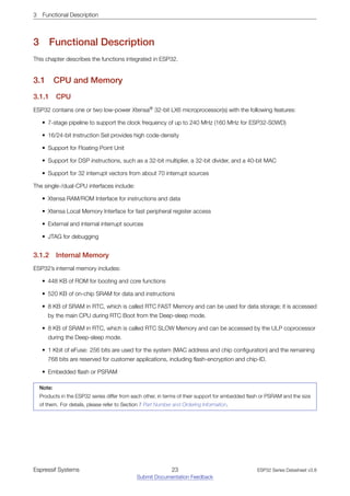
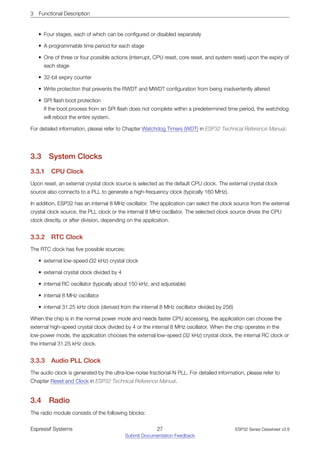
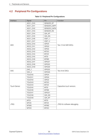
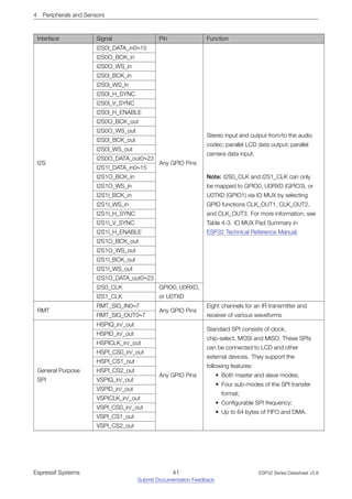
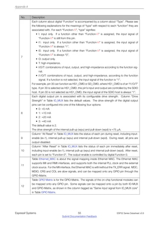
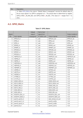
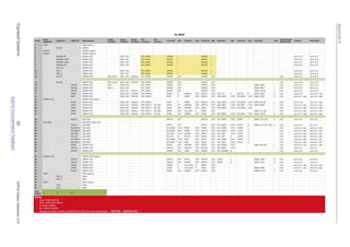
TXD[0](O) TXD[0](O) TXD[0](O) TXD[0](O)
GPIO22 EMAC_TXD1 TXD[1](O) TXD[1](O) TXD[1](O) TXD[1](O)
MTMS EMAC_TXD2 TXD[2](O) TXD[2](O) - -
MTDI EMAC_TXD3 TXD[3](O) TXD[3](O) - -
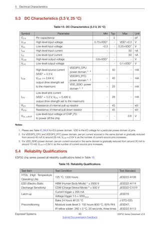
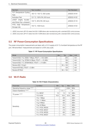
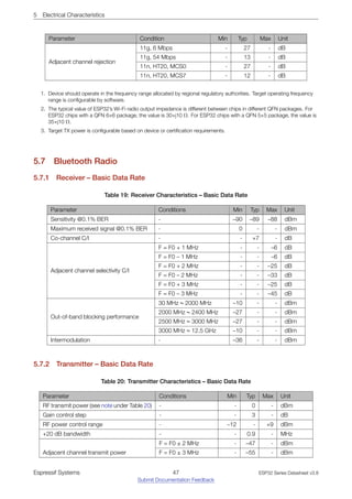
MTCK EMAC_RX_ER RX_ER(I) RX_ER(I) - -
GPIO27 EMAC_RX_DV RX_DV(I) RX_DV(I) CRS_DV(I) CRS_DV(I)
GPIO25 EMAC_RXD0 RXD[0](I) RXD[0](I) RXD[0](I) RXD[0](I)
GPIO26 EMAC_RXD1 RXD[1](I) RXD[1](I) RXD[1](I) RXD[1](I)
U0TXD EMAC_RXD2 RXD[2](I) RXD[2](I) - -
MTDO EMAC_RXD3 RXD[3](I) RXD[3](I) - -
GPIO16 EMAC_CLK_OUT CLK_OUT(O) - CLK_OUT(O) -
GPIO17 EMAC_CLK_OUT_180 CLK_OUT_180(O) - CLK_OUT_180(O) -
GPIO4 EMAC_TX_ER TX_ERR(O)* TX_ERR(O)* - -
In GPIO Matrix* - MDC(O) MDC(O) MDC(O) MDC(O)
In GPIO Matrix* - MDIO(IO) MDIO(IO) MDIO(IO) MDIO(IO)
In GPIO Matrix* - CRS(I) CRS(I) - -
In GPIO Matrix* - COL(I) COL(I) - -
*Notes: 1. The GPIO Matrix can be any GPIO. 2. The TX_ERR (O) is optional.
A.4. IO_MUX
For the list of IO_MUX pins, please see the next page.
Espressif Systems 61
Submit Documentation Feedback
ESP32 Series Datasheet v3.8