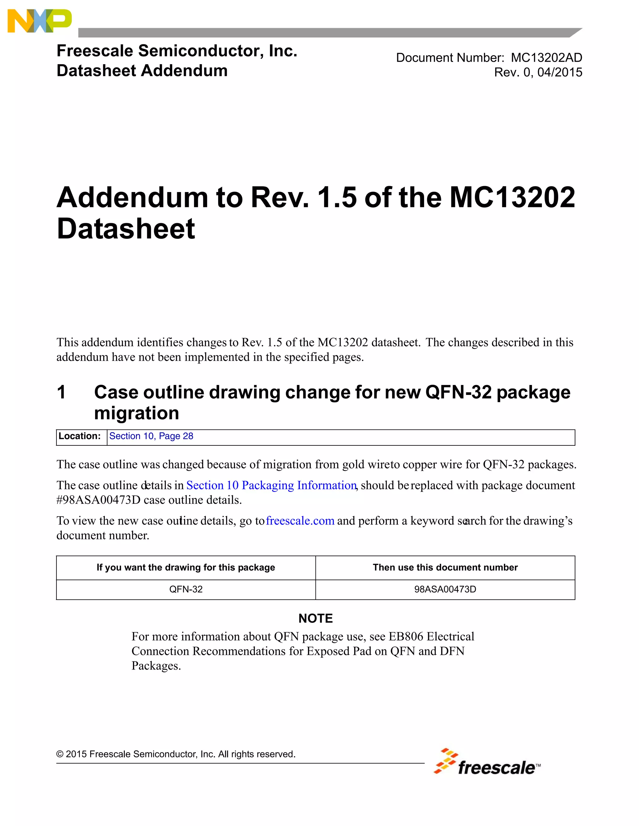
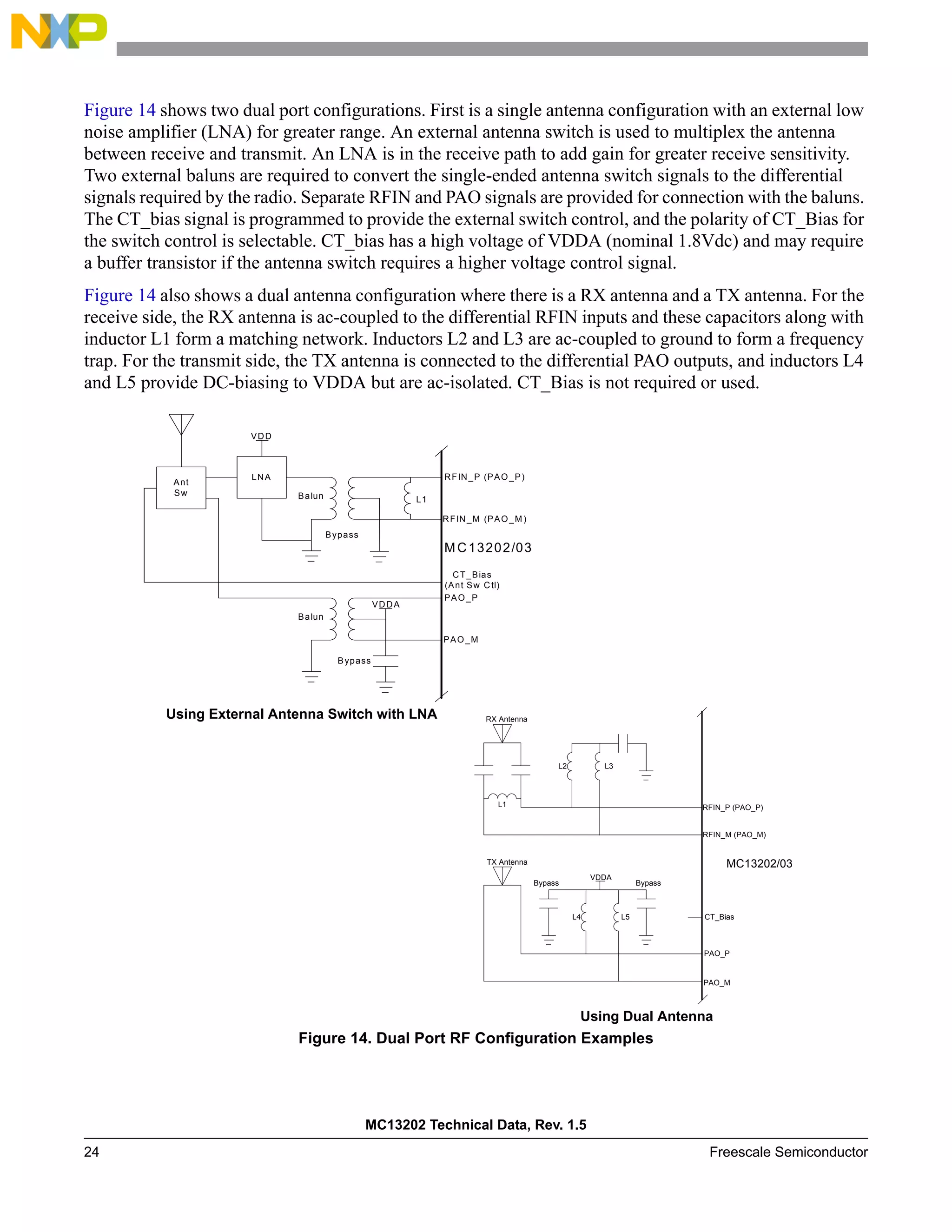
This document provides a summary of changes made in Revision 2 of the MC13202 datasheet from Freescale Semiconductor. The revision includes an addendum describing changes made to Revision 1.5, as well as the original Revision 1.5 datasheet. The addendum describes two changes: 1) a change to the case outline drawing for a new QFN-32 package, and 2) removal of references to case 1311-03. The full Revision 1.5 datasheet is then provided, describing the MC13202 low power transceiver chip.
Embedded World 2015: Sense2Go - 24GHz Sensor Solution for Industrial Applicat...Infineon4Engineers
With this slideshare presentation you will learn a lot about Infineon's Sense2Go Development Kit which provides everything for your own motion detection, door opener and warehouse smart lighting project.
The presentation is fully packed with detailed information about Infineon microcontroller, shows the Sense2Go evaluation boards, delivers a detailed snapshot of the Sense2Go PCB with all technical features and presents the complete roadmap for BGTxx ICs. Moreover you find the Infineon microcontroller portfolio which consists of XMC1100 on the lower end and XMC4500 at the upper end.
This document provides specifications for the ESP32 family of Wi-Fi and Bluetooth combo chips. It includes information on the chip's features such as integrated Wi-Fi and Bluetooth radios, dual-core CPUs, various peripherals, and low power modes. Revision histories and information on ordering parts are also included.
Microprocesador ESP32 manual de uso y programacionArturoYanezSG
This document provides specifications for the ESP32 family of Wi-Fi and Bluetooth combo chips. It includes information on the chip's features, pin definitions, functional description, electrical characteristics, and applications. Revision history and important documentation are also referenced.
This document describes the CC2530 system-on-chip solution, which integrates an RF transceiver, microcontroller, memory, and peripherals for low-power 2.4 GHz wireless applications. The CC2530 comes in versions with 32, 64, 128, or 256 KB of flash memory. It has various power modes allowing ultralow power consumption and supports IEEE 802.15.4, Zigbee, and RF4CE protocols. Development tools are available to help design wireless sensor networks, remote controls, lighting systems, and other low-power applications using the CC2530.
This product is a transceiver module designed for 2km optical communication applications. The design is compliant to 1000GBASE CWDM4 MSA standard. The module converts 4 inputs channels (ch) of 25Gb/s electrical data to 4 CWDM optical signals, and multiplexes them into a single channel for 100Gb/s optical transmission. Reversely, on the receiver side, the module optically de-multiplexes a 100Gb/s input into 4 CWDM channels signals, and converts them to 4 channel output electrical data.
The central wavelengths of the 4 CWDM channels are 1271, 1291, 1311 and 1331 nm as members of the CWDM wavelength grid defined in ITU-T G.694.2. It contains a duplex LC connector for the optical interface and a 38-pin connector for the electrical interface. To minimize the optical dispersion in the long-haul system, single-mode fiber (SMF) has to be applied in this module. Host FEC is required to support up to 2km fiber transmission.
The product is designed with form factor, optical/electrical connection and digital diagnostic interface according to the QSFP28 Multi-Source Agreement (MSA). It has been designed to meet the harshest external operating conditions including temperature, humidity and EMI interference.
The BlueOptics BO31J15680DC is a high performance 10Gbps optical receiver module that is fully compliant with XFP MSA standards. It supports transmission distances up to 80km on single mode fiber and provides real-time diagnostic monitoring of parameters like supply voltage, temperature, and received optical power. The module consists of a photodiode, transimpedance amplifier, laser driver, and digital diagnostic functions. It is hot-pluggable and offers industrial temperature ranges from -40C to 85C.
The document describes a 100Gb/s QSFP28 optical transceiver module that uses 4 independent full-duplex channels operating at up to 28Gb/s per channel. It has a QSFP28 form factor and interface and uses CWDM technology to transmit 4 wavelengths over a single fiber with up to 2km of reach. The module operates from a single 3.3V power supply and includes digital diagnostics and monitoring interfaces.
This document provides specifications for the ESP32 series of Wi-Fi and Bluetooth combo chips. It includes information on the chip's features such as its CPU, memory, radio capabilities, peripherals, and electrical characteristics. The document also includes pin definitions, package information, part numbers, and documentation resources.
The MSP430G2x53 and MSP430G2x13 are ultra-low power mixed signal microcontrollers from Texas Instruments with various features including low power consumption, integrated timers, analog comparator, and communication interfaces. They are available in different package and memory configurations suitable for applications such as low-cost sensor systems that capture analog signals and transmit processed digital data.
This document provides specifications for a 100Gb/s QSFP28 SR4 optical transceiver module. It has 4 independent channels with a maximum data rate of 28Gb/s per channel and 100m transmission over OM4 multi-mode fiber. Key features include low power consumption of 2.5W, operating temperature range of 0-70°C, and digital diagnostic monitoring via a 2-wire interface. Application areas include data center rack-to-rack connections and 100GbE.
The document describes an XFP 10G 1310nm optical receiver module that operates at 10Gbps over 10km of single mode fiber. It provides high-speed data transmission compliant with industry standards for applications such as Ethernet, Fibre Channel, SONET, and SDH. The module has diagnostic capabilities to monitor operating parameters and comes with a 5-year warranty.
BlueOptics Bo67hxx640d 2 4 8gbase dwdm xfp transceiver c band 40km singlemode...CBO GmbH
The document describes an XFP DWDM 8.5G C-Band optical transceiver module that operates at 8.5Gbps over 40km of single mode fiber. It contains an EML laser transmitter, PIN photodiode receiver, and digital diagnostic monitoring. The module complies with relevant interoperability standards and safety regulations, and offers various operating temperature ranges and wavelength channel options.
This document provides specifications for a BlueOptics BO67HXX680D XFP transceiver module that operates at 8.5 Gbps with a maximum range of 80 km on single mode fiber. It lists optical and electrical interface characteristics, applications, features, and ordering information for the various available temperature ranges and channels. Installation and regulatory compliance information is also included.
This document describes a project on automatic wireless power grid control. It is submitted by three students and guided by an assistant professor. The project uses a microcontroller to wirelessly control different units of a power grid based on time using an RF transmitter and receiver. It explains the hardware components used, including a power supply, diode bridge, microcontroller, RF modules, relay driver, encoder, decoder and LCD display. Block diagrams and working are provided, along with advantages of automation and potential applications in hardware control systems.
IGS-5225-4T2S, the smallest, fully-managed Gigabit fiber switch for harsh environments, features 4 10/100/1000Mbps copper ports, 2 100/1000X SFP ports and redundant power system in an IP30 rugged but compact-sized case. The IGS-5225-4T2S can be installed in any difficult environment as it can operate stably under the temperature range from -40 to 75 degrees C. With such a slim enclosure, it does not need a big space to install.
The switch features user-friendly yet advanced IPv6/IPv4 management interfaces, abundant L2/L4 switching functions and Layer 3 static routing capability. It allows either DIN-rail or wall mounting for efficient use of cabinet space. With 2 dual-speed SFP fiber slots, it can be flexibly applied to extend the connection distance.
Contact us
Tel: +91-7875432180 Email: sales@bbcpl.in
Website: https://www.bbcpl.in
NFCRFID Ripe for Application Expansion_ElectronicDesignHamed M. Sanogo
The document discusses near-field communication (NFC) and radio-frequency identification (RFID) technologies. It describes how NFC/RFID works using inductive coupling between a reader and passive tag. It then discusses how the MAX66242 integrated circuit can provide security features, energy harvesting capabilities, and an I2C interface to enable NFC/RFID in embedded applications. Examples of applications discussed include medical sensor tags, device configuration, and collecting diagnostic/error data wirelessly.
4 Channel Relay Board 5V-Bluetooth Compatible for ArduinoRaghav Shetty
Bluetooth technology is a short distance communication technology used by almost all phones
including smart phones and all laptops. This technology find very wide uses including that of Home &
Industrial automation.
The Relay shield is capable of controlling 4 relays. The max switching power could be
12A/250VAC or 15A/24VDC. It could be directly controlled by Arduino through digital IOs.
10Gb/s Tunable SFP+ Transceiver Hot Pluggable, Duplex LC, +3.3V, 100GHz, Mono...Allen He
SHPP-10G-Tun tunable SFP+ Optical Transceiver provides a high-speed serial link at 9.95 to 11.3 Gbps data rates. It
complies with SFP+ Multi-Source Agreement (MSA) Specification. It provides Digital diagnostics functions via a 2-wire serial
interface as specified in SFF-8472. It fulfills the tunable via the monolithically Mach-Zehnder Modulators (MZM) laser. It support optical link up to 80km for SONET/SDH, 10G FC and Ethernet applications.
The Cisco Nexus 3172TQ-32T is a 1 RU switch with 32 10GBASE-T ports and 6 QSFP+ ports, with a switching capacity of 1.4 Tbps and forwarding rate of up to 1 bpps. It has 4 GB of memory, 2 power supplies, and dimensions of 4.4 x 43.9 x 50.5 cm. To enable the remaining 16 10GBASE-T ports, a 16-port upgrade license must be installed.
This document describes a 10G 1554.13nm 40km DWDM SFP+ transceiver. It provides specifications for the transceiver including its data rate, supply voltage, operating temperature, optical and electrical characteristics, pin definitions, digital diagnostic monitoring interface, and dimensions. The transceiver is designed for 10 Gigabit Ethernet links up to 40km over single-mode fiber and supports 9.95-11.3 Gbps data rates while consuming less than 1.2W of power.
This document provides specifications for the DWDM-SFP10G-40-C58-T02 10G 1531.12nm 40km DWDM SFP+ transceiver. It includes details on its product description, features, functional diagram, optical and electrical characteristics, pin definitions, digital diagnostic monitoring interface, package dimensions and ordering information. The transceiver is designed for 10 Gigabit Ethernet links up to 40km over single-mode fiber and supports DWDM channels with 100GHz spacing and a center wavelength of 1531.12nm. It provides digital diagnostics monitoring of parameters such as temperature, voltages, optical powers and bias currents.
This document specifies the technical details of the DWDM-SFP10G-40-C56-T02 10G 1532.68nm 40km DWDM SFP+ transceiver. It includes specifications for optical and electrical characteristics, functional diagrams, pin definitions, digital diagnostic monitoring interface support, and dimensions. The transceiver is designed for 10GbE links up to 40km over single-mode fiber and supports real-time access to operating parameters via a 2-wire interface for monitoring.
This document describes an SFP 155M 1550nm optical transceiver module that operates at 155Mbps up to 120km on single mode fiber. It provides digital diagnostic functions and is compliant with RoHS and SFP MSA standards. Key features include a DFB laser transmitter, APD receiver, hot-pluggable SFP form factor, and operating temperature ranges from 0 to 85°C.
Blueoptics bo25k859s2d 40gbase-sr4 qsfp transceiver 4x850nm 150 meter multimo...CBO GmbH
This document describes a QSFP 40G 850nm 100M optical transceiver module. It provides high-level specifications including:
- It supports data rates up to 40Gbps over 100 meters of multi-mode fiber using 4 channels of VCSEL lasers and photodiodes.
- It complies with relevant QSFP and small form factor pluggable standards, and provides digital diagnostics over a 2-wire interface.
- Key features include hot-pluggability, metal enclosure, extended temperature range support, and 5-year warranty.
The DigiFlex® PerformanceTM Servo Drive DZRALTE-040L080 is a fully digital servo drive designed to drive brushed and brushless servomotors. It operates in torque, velocity, or position mode using space vector modulation for higher efficiency. The drive features configurable digital and analog inputs and outputs, RS-232 and RS-485 interfaces, and supports various command and feedback types. It is compliant with relevant safety standards and has a compact form factor making it suitable for embedded applications.
This document describes the specifications of a 10G 1534.25nm 40km DWDM SFP+ transceiver. It includes details on the product description, features, functional diagram, optical and electrical characteristics, pin definitions, digital diagnostic monitoring interface, package dimensions, and ordering information. The transceiver is designed for 10 Gigabit Ethernet links up to 40km over single-mode fiber and supports real-time monitoring of operating parameters through a digital diagnostic interface.
This document specifies the technical details of a 10G 1531.12nm 40km DWDM SFP+ transceiver. It includes specifications for the product's data rate, wavelength, power consumption, temperature range, diagnostic monitoring interface, pin definitions, optical and electrical characteristics, and dimensions. The transceiver uses a cooled EML laser transmitter and PIN photodiode receiver to operate over single-mode fiber for up to 40km at a bit rate between 9.95-11.3Gbps. It supports real-time monitoring via a standard 2-wire interface.
`The AN5277 is an integrated circuit (IC) amplifier widely used in audio applications, offering excellent audio quality and performance. Designed specifically for audio amplification, the AN5277 provides a compact and efficient solution for various audio systems, including portable devices, multimedia speakers, and automotive audio systems.
The document is a data sheet for the AD590 integrated circuit temperature transducer. It provides specifications for the device such as a linear current output of 1 μA/K, a temperature range of -55°C to +150°C, and a calibration accuracy of ±0.5°C. It also describes features of the device such as its 2-terminal design, wide power supply range, and sensor isolation from the case. Application examples include temperature measurement, compensation, and remote sensing.
The document describes the HT12D and HT12F decoders. The decoders receive serial addresses and data from encoders and decode the information. The HT12D provides 8 address bits and 4 data bits as outputs, while the HT12F decodes 12 address bits and provides a momentary valid transmission indicator. The decoders operate between 2.4-12V and require a resistor connected oscillator to function properly paired with Holtek encoders.
The document describes two CMOS LSIs, the HT12A and HT12E, which are encoders for remote control systems. They can encode information consisting of N address bits and 12-N data bits. The HT12A provides a 38kHz carrier for infrared transmission and allows selection of a data trigger, while the HT12E allows selection of a TE trigger. Upon receiving a trigger signal, the encoded addresses and data are transmitted in a series of words via an RF or infrared medium.
The document is a reference manual for the MFR4310 FlexRay controller. It provides an overview of the device, including its features, block diagram, signal descriptions, modes of operation and external interfaces. It also describes in detail the various modules within the FlexRay controller, including the FlexRay communication module, port integration module, voltage regulator and oscillator. The reference manual provides memory maps and detailed descriptions of the registers for configuration and control of the FlexRay controller functionality.
The TDA5051A is a modem IC designed for ASK data transmission over home power lines at 600 or 1200 baud. It features fully digital carrier generation and modulation/demodulation, with an integrated output power stage. The IC requires few external components and operates from a single 5V supply. It is intended for applications such as home automation, energy control, and transmitting data over power lines using amplitude shift keying modulation at carrier frequencies up to 132.5 kHz.
This document provides an overview and evaluation of the A5191HRTNGEVB evaluation board, which demonstrates the external components needed for operating the A5191HRT IC for HART communications. The board allows testing the IC's small PCB footprint and easy design of HART implementations. Key sections described include the power supply, reference voltages, clock generation, and schematic. Electrical characteristics and a bill of materials are also provided.
Google Calendar is a versatile tool that allows users to manage their schedules and events effectively. With Google Calendar, you can create and organize calendars, set reminders for important events, and share your calendars with others. It also provides features like creating events, inviting attendees, and accessing your calendar from mobile devices. Additionally, Google Calendar allows you to embed calendars in websites or platforms like SlideShare, making it easier for others to view and interact with your schedules.
The Indian government has been working over the past few years to include elements of ITS in the transport sector. This standard ensures the optimal operation of the current transport infrastructure. It also increases the efficiency, safety, comfort, and quality of the system. That is why the government created the AIS-140 standard. Compliance with this standard means all vehicles used for public transit must have panic buttons and vehicle tracking modules installed. Nevertheless, in future in the standard protocol of AIS-140 you can expect fare collection and CCTV capabilities.
Get more information here: https://blog.watsoo.com/2023/12/27/all-about-prithvi-ais-140-gps-vehicle-tracker/
3. Addendum to MC13201 Technical Data, Rev. 1.3
Freescale Semiconductor, Inc. 3
References to case 1311-03
2 References to case 1311-03
Remove the references to case 1311-03.
Location:
Section 1, Page 1
Section 10, Page 28
5. MC13202 Technical Data, Rev. 1.5
2 Freescale Semiconductor
more detailed information about MC13202 operation, refer to the MC13202 Reference Manual,
(MC13202RM).
Applications include, but are not limited to, the following:
• Residential and commercial automation
— Lighting control
— Security
— Access control
— Heating, ventilation, air-conditioning (HVAC)
— Automated meter reading (AMR)
• Industrial Control
— Asset tracking and monitoring
— Homeland security
— Process management
— Environmental monitoring and control
— HVAC
— Automated meter reading
• Health Care
— Patient monitoring
— Fitness monitoring
• Consumer
— Human interface devices (keyboard, mice, etc.)
— Remote control
— Wireless toys
The transceiver includes a low noise amplifier, 1.0 mW power amplifiers (PA), onboard RF
transmit/receive (T/R) switch for single port use, PLL with internal voltage controlled oscillator (VCO),
on-board power supply regulation, and full spread-spectrum encoding and decoding. The device supports
250 kbps Offset-Quadrature Phase Shift Keying (O-QPSK) data in 2.0 MHz channels with 5.0 MHz
channel spacing per the 802.15.4 Standard. The SPI port and interrupt request output are used for receive
(RX) and transmit (TX) data transfer and control.
2 Features
• Recommended power supply range: 2.0 to 3.4 V
• Fully compliant 802.15.4 Standard transceiver supports 250 kbps O-QPSK data in 5.0 MHz
channels and full spread-spectrum encode and decode
• Operates on one of 16 selectable channels in the 2.4 GHz band
• -1 to 0 dBm nominal output power, programmable from -27 dBm to +3 dBm typical
• Receive sensitivity of <-92 dBm (typical) at 1% PER, 20-byte packet, much better than the
802.15.4 Standard of -85 dBm
6. MC13202 Technical Data, Rev. 1.5
Freescale Semiconductor 3
• Integrated transmit/receive switch
• Dual PA output pairs which can be programmed for full differential single port or dual port
operation that supports an external LNA and/or PA
• Three power down modes for increased battery life
— < 1 µA Off current
— 1.0 µA Typical Hibernate current
— 35 µA Typical Doze current (no CLKO)
• Programmable frequency clock output (CLKO) for use by MCU
• Onboard trim capability for 16 MHz crystal reference oscillator eliminates need for external
variable capacitors and allows for automated production frequency calibration
• Four internal timer comparators available to supplement MCU timer resources
• Supports both Packet Mode and Streaming Mode data transfer
• Buffered transmit and receive data packets for simplified use with low cost MCUs
• Seven GPIO to supplement MCU GPIO
• Operating temperature range: -40 °C to 85 °C
• Small form factor QFN-32 Package
— Meets moisture sensitivity level (MSL) 3
— 260 °C peak reflow temperature
— Meets lead-free requirements
2.1 Software Features
Freescale provides a wide range of software functionality to complement the MC13202 hardware. There
are three levels of application solutions:
1. Simple proprietary wireless connectivity.
2. User networks built on the 802.15.4 MAC standard.
3. ZigBee-compliant network stack.
2.1.1 Simple MAC (SMAC)
• Small memory footprint (about 3 Kbytes typical)
• Supports point-to-point and star network configurations
• Proprietary networks
• Source code and application examples provided
7. MC13202 Technical Data, Rev. 1.5
4 Freescale Semiconductor
2.1.2 802.15.4 Standard-Compliant MAC
• Supports star, mesh and cluster tree topologies
• Supports beaconed networks
• Supports GTS for low latency
• Multiple power saving modes (idle doze, hibernate)
2.1.3 ZigBee-Compliant Network Stack
• Supports all ZigBee specifications
• Supports star, mesh and tree networks
• Advanced Encryption Standard (AES) 128-bit security
3 Block Diagrams
Figure 1 shows a simplified block diagram of the MC13202 which is an 802.15.4 Standard compatible
transceiver that provides the functions required in the physical layer (PHY) specification.
Figure 1. 802.15.4 Modem Simplified Block Diagram
Phase Shift Modulator
RST
GPIO1
GPIO2
GPIO3
GPIO4
XTAL2
XTAL1
RFIN_M
(PAO_M)
PAO_P
PAO_M
MOSI
MISO
SPICLK
RXTXEN
CE
ATTN
GPIO5
GPIO6
GPIO7
Receive
Packet RAM
Transmit
Packet RAM 1
Transmit RAM
Arbiter
Receive RAM
Arbiter
PA
VCO
Crystal
Oscillator
Symbol
Generation
FCS
Generation
Header
Generation
MUX
Sequence
Manager
(Control Logic)
VDDLO2 ÷4
256 MHz
2.45 GHz
LNA
1st IF Mixer
IF = 65 MHz
2nd IF Mixer
IF = 1 MHz PMA
Decimation
Filter
Matched
Filter
Baseband
Mixer
DCD
Correlator
Symbol
Synch
&
Det
CCA
Packet
Processor
IRQ
Arbiter
24 Bit Event Timer
IRQ
16 MHz
AGC
Analog
Regulator VBATT
Digital
Regulator L
Digital
Regulator H
Power-Up
Control
Logic
Crystal
Regulator
VCO
Regulator
VDDINT
Programmable
Prescaler
CLKO
4 Programmable
Timer Comparators
Synthesizer
VDDD
VDDVCO
SERIAL
PERIPHERAL
INTERFACE
(SPI)
VDDA
VDDLO1
Transmit
Packet RAM 2
T / R
RFIN_P
(PAO_P)
CT_Bias
8. MC13202 Technical Data, Rev. 1.5
Freescale Semiconductor 5
Figure 2 shows the basic system block diagram for the MC13202 in an application. Interface with the
transceiver is accomplished through a 4-wire SPI port and interrupt request line. The media access control
(MAC), drivers, and network and application software (as required) reside on the host processor. The host
can vary from a simple 8-bit device up to a sophisticated 32-bit processor depending on application
requirements.
Figure 2. System Level Block Diagram
4 Data Transfer Modes
The MC13202 has two data transfer modes:
1. Packet Mode — Data is buffered in on-chip RAM
2. Streaming Mode — Data is processed word-by-word
The Freescale 802.15.4 MAC software only supports the streaming mode of data transfer. For proprietary
applications, packet mode can be used to conserve MCU resources.
4.1 Packet Structure
Figure 3 shows the packet structure of the MC13202. Payloads of up to 125 bytes are supported. The
MC13202 adds a four-byte preamble, a one-byte Start of Frame Delimiter (SFD), and a one-byte Frame
Length Indicator (FLI) before the data. A Frame Check Sequence (FCS) is calculated and appended to the
end of the data.
Figure 3. MC13202 Packet Structure
Analog Receiver
MC13202
Frequency
Generation
Analog
Transmitter
Voltage
Regulators
Power Up
Management
Control
Logic
Buffer RAM
Digital
Transceiver
SPI
and GPIO
Microcontroller
SPI
ROM
(Flash)
RAM
CPU A/D
Timer
Application
IRQ
Arbiter
RAM
Arbiter
Timer
Network
MAC
PHY Driver
Preamble SFD FLI Payload Data FCS
4 bytes 1 byte 1 byte 125 bytes maximum 2 bytes
9. MC13202 Technical Data, Rev. 1.5
6 Freescale Semiconductor
4.2 Receive Path Description
In the receive signal path, the RF input is converted to low IF In-phase and Quadrature (I & Q) signals
through two down-conversion stages. A Clear Channel Assessment (CCA) can be performed based upon
the baseband energy integrated over a specific time interval. The digital backend performs Differential
Chip Detection (DCD), the correlator “de-spreads” the Direct Sequence Spread Spectrum (DSSS) Offset
QPSK (O-QPSK) signal, determines the symbols and packets, and detects the data.
The preamble, SFD, and FLI are parsed and used to detect the payload data and FCS which are stored in
RAM. A two-byte FCS is calculated on the received data and compared to the FCS value appended to the
transmitted data, which generates a Cyclical Redundancy Check (CRC) result. Link Quality is measured
over a 64 µs period after the packet preamble and stored in RAM.
If the MC13202 is in packet mode, the data is processed as an entire packet. The MCU is notified that an
entire packet has been received via an interrupt.
If the MC13202 is in streaming mode, the MCU is notified by an interrupt on a word-by-word basis.
Figure 4 shows CCA reported power level versus input power. Note that CCA reported power saturates at
about -57 dBm input power which is well above 802.15.4 Standard requirements. Figure 5 shows energy
detection/LQI reported level versus input power.
NOTE
For both graphs, the required 802.15.4 Standard accuracy and range limits
are shown. A 3.5 dBm offset has been programmed into the CCA reporting
level to center the level over temperature in the graphs.
Figure 4. Reported Power Level versus Input Power in CCA Mode
-100
-90
-80
-70
-60
-50
-90 -80 -70 -60 -50
Input Pow er (dBm)
Reported
Power
Level
(dBm)
802.15.4 Accuracy
and range Requirements
10. MC13202 Technical Data, Rev. 1.5
Freescale Semiconductor 7
Figure 5. Reported Power Level Versus Input Power for Energy Detect or Link Quality Indicator
4.3 Transmit Path Description
For the transmit path, the TX data that was previously stored in RAM is retrieved (packet mode) or the TX
data is clocked in via the SPI (stream mode), formed into packets per the 802.15.4 PHY, spread, and then
up-converted to the transmit frequency.
If the MC13202 is in packet mode, data is processed as an entire packet. The data are first loaded into the
TX buffer. The MCU then requests that the MC13202 transmit the data. The MCU is notified via an
interrupt when the whole packet has successfully been transmitted.
In streaming mode, the data is fed to the MC13202 on a word-by-word basis with an interrupt serving as
a notification that the MC13202 is ready for more data. This continues until the whole packet is
transmitted.
-85
-75
-65
-55
-45
-35
-25
-15
-85 -75 -65 -55 -45 -35 -25 -15
Input Power Level (dBm)
Reported
Power
Level
(dBm)
802.15.4 Accuracy
and Range Requirements
11. MC13202 Technical Data, Rev. 1.5
8 Freescale Semiconductor
5 Electrical Characteristics
5.1 Maximum Ratings
5.2 Recommended Operating Conditions
Table 1. Maximum Ratings
Rating Symbol Value Unit
Power Supply Voltage VBATT, VDDINT -0.3 to 3.6 Vdc
Digital Input Voltage Vin -0.3 to (VDDINT + 0.3)
RF Input Power Pmax 10 dBm
Junction Temperature TJ 125 °C
Storage Temperature Range Tstg -55 to 125 °C
Note: Maximum Ratings are those values beyond which damage to the device may occur.
Functional operation should be restricted to the limits in the Electrical Characteristics
or Recommended Operating Conditions tables.
Note: Meets Human Body Model (HBM) = 2 kV. RF input/output pins have no ESD protection.
Table 2. Recommended Operating Conditions
Characteristic Symbol Min Typ Max Unit
Power Supply Voltage (VBATT = VDDINT)1
1
If the supply voltage is produced by a switching DC-DC converter, ripple should be less than 100 mV peak-to-peak.
VBATT,
VDDINT
2.0 2.7 3.4 Vdc
Input Frequency fin 2.405 - 2.480 GHz
Ambient Temperature Range TA -40 25 85 °C
Logic Input Voltage Low VIL 0 - 30%
VDDINT
V
Logic Input Voltage High VIH 70%
VDDINT
- VDDINT V
SPI Clock Rate fSPI - - 8.0 MHz
RF Input Power Pmax - - 10 dBm
Crystal Reference Oscillator Frequency (±40 ppm over
operating conditions to meet the 802.15.4 Standard.)
fref 16 MHz Only
12. MC13202 Technical Data, Rev. 1.5
Freescale Semiconductor 9
5.3 DC Electrical Characteristics
Table 3. DC Electrical Characteristics
(VBATT, VDDINT = 2.7 V, TA = 25 °C, unless otherwise noted)
Characteristic Symbol Min Typ Max Unit
Power Supply Current (VBATT + VDDINT)
Off1
Hibernate1
Doze (No CLKO)1 2
Idle
Transmit Mode (0 dBm nominal output power)
Receive Mode
1
To attain specified low power current, all GPIO and other digital IO must be handled properly. See Section 8.3, “Low
Power Considerations”.
2
CLKO frequency at default value of 32.786 kHz.
Ileakage
ICCH
ICCD
ICCI
ICCT
ICCR
-
-
-
-
-
-
0.2
1.0
35
500
30
37
1.0
6.0
102
800
35
42
µA
µA
µA
µA
mA
mA
Input Current (VIN = 0 V or VDDINT) (All digital inputs) IIN - - ±1 µA
Input Low Voltage (All digital inputs) VIL 0 - 30%
VDDINT
V
Input High Voltage (all digital inputs) VIH 70%
VDDINT
- VDDINT V
Output High Voltage (IOH = -1 mA) (All digital outputs) VOH 80%
VDDINT
- VDDINT V
Output Low Voltage (IOL = 1 mA) (All digital outputs) VOL 0 - 20%
VDDINT
V
13. MC13202 Technical Data, Rev. 1.5
10 Freescale Semiconductor
5.4 AC Electrical Characteristics
Table 4. Receiver AC Electrical Characteristics
(VBATT, VDDINT = 2.7 V, TA = 25 °C, fref = 16 MHz, unless otherwise noted.)
Characteristic Symbol Min Typ Max Unit
Sensitivity for 1% Packet Error Rate (PER) (-40 to +85 °C) SENSper - -92 - dBm
Sensitivity for 1% Packet Error Rate (PER) (+25 °C) - -92 -87 dBm
Saturation (maximum input level) SENSmax - 10 - dBm
Channel Rejection for dual port mode (1% PER and desired signal -82 dBm)
+5 MHz (adjacent channel)
-5 MHz (adjacent channel)
+10 MHz (alternate channel)
-10 MHz (alternate channel)
>= 15 MHz
-
-
-
-
-
31
30
43
41
53
-
-
-
-
-
dB
dB
dB
dB
dB
Frequency Error Tolerance - - 200 kHz
Symbol Rate Error Tolerance - - 80 ppm
Table 5. Transmitter AC Electrical Characteristics
(VBATT, VDDINT = 2.7 V, TA = 25 °C, fref = 16 MHz, unless otherwise noted.)
Characteristic Symbol Min Typ Max Unit
Power Spectral Density (-40 to +85 °C) Absolute limit - -47 - dBm
Power Spectral Density (-40 to +85 °C) Relative limit - 47 -
Nominal Output Power1
1
SPI Register 12 programmed to 0x00BC which sets output power to nominal (-1 dBm typical).
Pout -4 -1 2 dBm
Maximum Output Power2
2 SPI Register 12 programmed to 0x00FF which sets output power to maximum.
4 dBm
Error Vector Magnitude EVM - 20 35 %
Output Power Control Range - 30 - dB
Over the Air Data Rate - 250 - kbps
2nd Harmonic3
3 Measured with output power set to nominal (0 dBm) and temperature @ 25 °C
- -48 - dBc
3rd Harmonic3
- -70 - dBc
14. MC13202 Technical Data, Rev. 1.5
Freescale Semiconductor 11
Figure 6 shows an RF parameter evaluation circuit.
Figure 6. RF Parametric Evaluation Circuit
Table 6. Digital Timing Specifications
(VBATT, VDDINT = 2.7 V, TA = 25 °C, frequency = 16 MHz, unless otherwise noted.
SPI timing parameters are referenced to Figure 8.
Symbol Parameter Min Typ Max Unit
T0 SPICLK period 125 nS
T1 Pulse width, SPICLK low 50 nS
T2 Pulse width, SPICLK high 50 nS
T3 Delay time, MISO data valid from falling SPICLK 15 nS
T4 Setup time, CE low to rising SPICLK 15 nS
T5 Delay time, MISO valid from CE low 15 nS
T6 Setup time, MOSI valid to rising SPICLK 15 nS
T7 Hold time, MOSI valid from rising SPICLK 15 nS
RST minimum pulse width low (asserted) 250 nS
Table 7. RF Port Impedance
Characteristic Symbol Typ Unit
RFIN Pins for internal T/R switch configuration, TX mode
2.405 GHz
2.442 GHz
2.480 GHz
Zin 16.1 - j126
16.0 – j123
15.8 – j121
Ω
RFIN Pins for internal or external T/R switch configuration, RX mode
2.405 GHz
2.442 GHz
2.480 GHz
Zin 14.4 – j77.2
14.5 – j74.8
14.6 – j72.5
Ω
PAO Pins for external T/R switch configuration, TX mode
2.405 GHz
2.442 GHz
2.480 GHz
Zin 18.5 – j148
18.3 – j146
18.2 – j143
Ω
5
1
6
2
3
4
Z4
LDB212G4005C-001
L10
4.7nH
L11
4.7nH
C12
10pF
VDDA
VDD
6
IN
5
VCONT
4
OUT1
1 OUT2
3
GND
2
IC2
µPG2012TK-E2
C13
10pF
C14
10pF
5
1
6
2
3
4
Z5
LDB212G4005C-001
L12
2.2nH
C15
1.8pF
1
2
5
3
4
J3
SMA_edge_Receptacle_Female
L13
3.3nH
L14
3.3nH
C16
10pF
C17
1.0pF
C18
1.8pF
GPIO1
44
PAO_M
39
PAO_P
38
RFIN_P
36
RFIN_M
35
CT_Bias
34
U4
MC1320x
15. MC13202 Technical Data, Rev. 1.5
12 Freescale Semiconductor
6 Functional Description
The following sections provide a detailed description of the MC13202 functionality including the
operating modes and Serial Peripheral Interface (SPI).
6.1 MC13202 Operational Modes
The MC13202 has a number of operational modes that allow for low-current operation. Transition from
the Off to Idle mode occurs when RST is negated. Once in Idle, the SPI is active and is used to control the
IC. Transition to Hibernate and Doze modes is enabled via the SPI. These modes are summarized, along
with the transition times, in Table 8. Current drain in the various modes is listed in Table 3, DC Electrical
Characteristics.
6.2 Serial Peripheral Interface (SPI)
The host microcontroller directs the MC13202, checks its status, and reads/writes data to the device
through the 4-wire SPI port. The transceiver operates as a SPI slave device only. A transaction between
the host and the MC13202 occurs as multiple 8-bit bursts on the SPI. The SPI signals are:
1. Chip Enable (CE) - A transaction on the SPI port is framed by the active low CE input signal. A
transaction is a minimum of 3 SPI bursts and can extend to a greater number of bursts.
2. SPI Clock (SPICLK) - The host drives the SPICLK input to the MC13202. Data is clocked into the
master or slave on the leading (rising) edge of the return-to-zero SPICLK and data out changes
state on the trailing (falling) edge of SPICLK.
NOTE
For Freescale microcontrollers, the SPI clock format is the clock phase
control bit CPHA = 0 and the clock polarity control bit CPOL = 0.
3. Master Out/Slave In (MOSI) - Incoming data from the host is presented on the MOSI input.
4. Master In/Slave Out (MISO) - The MC13202 presents data to the master on the MISO output.
Table 8. MC13202 Mode Definitions and Transition Times
Mode Definition
Transition Time
To or From Idle
Off All IC functions Off, Leakage only. RST asserted. Digital outputs are tri-stated
including IRQ
10 - 25 ms to Idle
Hibernate Crystal Reference Oscillator Off. (SPI not functional.) IC Responds to ATTN. Data is
retained.
7 - 20 ms to Idle
Doze Crystal Reference Oscillator On but CLKO output available only if Register 7, Bit 9 =
1 for frequencies of 1 MHz or less. (SPI not functional.) Responds to ATTN and can
be programmed to enter Idle Mode through an internal timer comparator.
(300 + 1/CLKO) µs to Idle
Idle Crystal Reference Oscillator On with CLKO output available. SPI active.
Receive Crystal Reference Oscillator On. Receiver On. 144 µs from Idle
Transmit Crystal Reference Oscillator On. Transmitter On. 144 µs from Idle
16. MC13202 Technical Data, Rev. 1.5
Freescale Semiconductor 13
A typical interconnection to a microcontroller is shown in Figure 7.
Figure 7. SPI Interface
Although the SPI port is fully static, internal memory, timer and interrupt arbiters require an internal clock
(CLKcore), derived from the crystal reference oscillator, to communicate from the SPI registers to internal
registers and memory.
6.2.1 SPI Burst Operation
The SPI port of an MCU transfers data in bursts of 8 bits with most significant bit (MSB) first. The master
(MCU) can send a byte to the slave (transceiver) on the MOSI line and the slave can send a byte to the
master on the MISO line. Although an MC13202 transaction is three or more SPI bursts long, the timing
of a single SPI burst is shown in Figure 8.
Figure 8. SPI Single Burst Timing Diagram
SPI digital timing specifications are shown in Table 6.
Shift Register
Baud Rate
Generator
Shift Register
Chip Enable (CE)
RxD MISO
TxD MOSI
Sclk SPICLK
MCU MC13202
CE
1 2 3 4 5 6 7 8
CE
SPICLK
T1
T2
T4
T0
SPI Burst
Valid
T5
T6
T3
Valid
T7
MISO
MOSI
Valid
17. MC13202 Technical Data, Rev. 1.5
14 Freescale Semiconductor
6.2.2 SPI Transaction Operation
Although the SPI port of an MCU transfers data in bursts of 8 bits, the MC13202 requires that a complete
SPI transaction be framed by CE, and there will be three (3) or more bursts per transaction. The assertion
of CE to low signals the start of a transaction. The first SPI burst is a write of an 8-bit header to the
transceiver (MOSI is valid) that defines a 6-bit address of the internal resource being accessed and
identifies the access as being a read or write operation. In this context, a write is data written to the
MC13202 and a read is data written to the SPI master. The following SPI bursts will be either the write
data (MOSI is valid) to the transceiver or read data from the transceiver (MISO is valid).
Although the SPI bus is capable of sending data simultaneously between master and slave, the MC13202
never uses this mode. The number of data bytes (payload) will be a minimum of 2 bytes and can extend to
a larger number depending on the type of access. The number of payload bytes sent will always be an even
integer. After the final SPI burst, CE is negated to high to signal the end of the transaction. Refer to the
MC13202 Reference Manual, (MC13202RM) for more details on SPI registers and transaction types.
An example SPI read transaction with a 2-byte payload is shown in Figure 9.
Figure 9. SPI Read Transaction Diagram
C E
SPIC L K
M ISO
M O SI V alid
V alid V alid
C lock B urst
H eader R ead data
18. MC13202 Technical Data, Rev. 1.5
Freescale Semiconductor 15
7 Pin Connections
Table 8. Pin Function Description
Pin # Pin Name Type Description Functionality
1 RFIN_M RF Input RF input/output negative. When used with internal T/R switch, this is
a bi-directional RF port for the internal LNA
and PA
2 RFIN_P RF Input RF input/output positive. When used with internal T/R switch, this is
a bi-directional RF port for the internal LNA
and PA
3 CT_Bias Control voltage Bias voltage/control signal for external
RF components
When used with internal T/R switch,
provides RX ground reference and TX
VDDA reference for use with external
balun. Can also be used as a control signal
for external LNA, PA, or T/R switch.
4 NC Tie to Ground.
5 PAO_P RF Output /DC Input RF Power Amplifier Output Positive. Open drain. Connect to VDDA through a
bias network when used with an external
balun. Not used when internal T/R switch is
used.
6 PAO_M RF Output/DC Input RF Power Amplifier Output Negative. Open drain. Connect to VDDA through a
bias network when used with an external
balun. Not used when internal T/R switch is
used.
7 SM Input Test mode pin. Must be grounded for normal operation.
8 GPIO41 Digital Input/ Output General Purpose Input/Output 4. See Footnote 1
9 GPIO31 Digital Input/ Output General Purpose Input/Output 3. See Footnote 1
10 GPIO21 Digital Input/ Output General Purpose Input/Output 2.
When gpio_alt_en, Register 9, Bit 7 =
1, GPIO2 functions as a “CRC Valid”
indicator.
See Footnote 1
11 GPIO11 Digital Input/ Output General Purpose Input/Output 1.
When gpio_alt_en, Register 9, Bit 7 =
1, GPIO1 functions as an “Out of Idle”
indicator.
See Footnote 1
12 RST Digital Input Active Low Reset. While held low, the
IC is in Off Mode and all internal
information is lost from RAM and SPI
registers. When high, IC goes to IDLE
Mode, with SPI in default state.
19. MC13202 Technical Data, Rev. 1.5
16 Freescale Semiconductor
13 RXTXEN2
Digital Input Active High. Low to high transition
initiates RX or TX sequence
depending on SPI setting. Should be
taken high after SPI programming to
start RX or TX sequence and should
be held high through the sequence.
After sequence is complete, return
RXTXEN to low. When held low,
forces Idle Mode.
See Footnote 2
14 ATTN2
Digital Input Active Low Attention. Transitions IC
from either Hibernate or Doze Modes
to Idle.
See Footnote 2
15 CLKO Digital Output Clock output to host MCU.
Programmable frequencies of:
16 MHz, 8 MHz, 4 MHz, 2 MHz, 1
MHz, 62.5 kHz, 32.786+ kHz
(default),
and 16.393+ kHz.
16 SPICLK2 Digital Clock Input External clock input for the SPI
interface.
See Footnote 2
17 MOSI2
Digital Input Master Out/Slave In. Dedicated SPI
data input.
See Footnote 2
18 MISO3
Digital Output Master In/Slave Out. Dedicated SPI
data output.
See Footnote 3
19 CE2 Digital Input Active Low Chip Enable. Enables SPI
transfers.
See Footnote 2
20 IRQ Digital Output Active Low Interrupt Request. Open drain device.
Programmable 40 kΩ internal pull-up.
Interrupt can be serviced every 6 µs with
<20 pF load.
Optional external pull-up must be >4 kΩ.
21 VDDD Power Output Digital regulated supply bypass. Decouple to ground.
22 VDDINT Power Input Digital interface supply & digital
regulator input. Connect to Battery.
2.0 to 3.4 V. Decouple to ground.
23 GPIO51 Digital Input/Output General Purpose Input/Output 5. See Footnote 1
24 GPIO61 Digital Input/Output General Purpose Input/Output 6. See Footnote 1
25 GPIO71 Digital Input/Output General Purpose Input/Output 7. See Footnote 1
26 XTAL1 Input Crystal Reference oscillator input. Connect to 16 MHz crystal and load
capacitor.
Table 8. Pin Function Description (continued)
Pin # Pin Name Type Description Functionality
20. MC13202 Technical Data, Rev. 1.5
Freescale Semiconductor 17
27 XTAL2 Input/Output Crystal Reference oscillator output
Note: Do not load this pin by using it
as a 16 MHz source. Measure
16 MHz output at Pin 15,
CLKO, programmed for 16
MHz. See the MC13202
Reference Manual for details.
Connect to 16 MHz crystal and load
capacitor.
28 VDDLO2 Power Input LO2 VDD supply. Connect to VDDA
externally.
29 VDDLO1 Power Input LO1 VDD supply. Connect to VDDA
externally.
30 VDDVCO Power Output VCO regulated supply bypass. Decouple to ground.
31 VBATT Power Input Analog voltage regulators Input.
Connect to Battery.
Decouple to ground.
32 VDDA Power Output Analog regulated supply Output.
Connect to directly VDDLO1 and
VDDLO2 externally and to PAO±
through a bias network.
Note: Do not use this pin to supply
circuitry external to the chip.
Decouple to ground. Only active high when
CCA, RX, or TX sequences in progress.
EP Ground External paddle / flag ground. Connect to ground.
1
The transceiver GPIO pins default to inputs at reset. There are no programmable pullups on these pins. Unused GPIO pins
should be tied to ground if left as inputs, or if left unconnected, they should be programmed as outputs set to the low state.
2
During low power modes, input must remain driven by MCU.
3
By default MISO is tri-stated when CE is negated. For low power operation, miso_hiz_en (Bit 11, Register 07) should be set
to zero so that MISO is driven low when CE is negated.
Table 8. Pin Function Description (continued)
Pin # Pin Name Type Description Functionality
22. MC13202 Technical Data, Rev. 1.5
Freescale Semiconductor 19
8 Crystal Oscillator Reference Frequency
This section provides application specific information regarding crystal oscillator reference design and
recommended crystal usage.
8.1 Crystal Oscillator Design Considerations
The 802.15.4 Standard requires that several frequency tolerances be kept within ± 40 ppm accuracy. This
means that a total offset up to 80 ppm between transmitter and receiver will still result in acceptable
performance. The MC13202 transceiver provides onboard crystal trim capacitors to assist in meeting this
performance.
The primary determining factor in meeting this specification is the tolerance of the crystal oscillator
reference frequency. A number of factors can contribute to this tolerance and a crystal specification will
quantify each of them:
1. The initial (or make) tolerance of the crystal resonant frequency itself.
2. The variation of the crystal resonant frequency with temperature.
3. The variation of the crystal resonant frequency with time, also commonly known as aging.
4. The variation of the crystal resonant frequency with load capacitance, also commonly known as
pulling. This is affected by:
a) The external load capacitor values - initial tolerance and variation with temperature.
b) The internal trim capacitor values - initial tolerance and variation with temperature.
c) Stray capacitance on the crystal pin nodes - including stray on-chip capacitance, stray package
capacitance and stray board capacitance; and its initial tolerance and variation with
temperature.
5. Whether or not a frequency trim step will be performed in production
Freescale requires the use of a 16 MHz crystal with a <9 pF load capacitance. The MC13202 does not
contain a reference divider, so 16 MHz is the only frequency that can be used. A crystal requiring higher
load capacitance is prohibited because a higher load on the amplifier circuit may compromise its
performance. The crystal manufacturer defines the load capacitance as that total external capacitance seen
across the two terminals of the crystal. The oscillator amplifier configuration used in the MC13202
requires two balanced load capacitors from each terminal of the crystal to ground. As such, the capacitors
are seen to be in series by the crystal, so each must be <18 pF for proper loading.
In the Figure 11 crystal reference schematic, the external load capacitors are shown as 6.8 pF each, used
in conjunction with a crystal that requires an 8 pF load capacitance. The default internal trim capacitor
value (2.4 pF) and stray capacitance total value (6.8 pF) sum up to 9.2 pF giving a total of 16 pF. The value
for the stray capacitance was determined empirically assuming the default internal trim capacitor value and
for a specific board layout. A different board layout may require a different external load capacitor value.
The on-chip trim capability may be used to determine the closest standard value by adjusting the trim value
via the SPI and observing the frequency at CLKO. Each internal trim load capacitor has a trim range of
approximately 5 pF in 20 fF steps.
23. MC13202 Technical Data, Rev. 1.5
20 Freescale Semiconductor
Figure 11. MC13202 Modem Crystal Circuit
Initial tolerance for the internal trim capacitance is approximately ±15%.
Since the MC13202 contains an on-chip reference frequency trim capability, it is possible to trim out
virtually all of the initial tolerance factors and put the frequency within 0.12 ppm on a board-by-board
basis. Individual trimming of each board in a production environment allows use of the lowest cost crystal,
but requires that each board go through a trimming procedure. This step can be avoided by
using/specifying a crystal with a tighter stability tolerance, but the crystal will be slightly higher in cost.
A tolerance analysis budget may be created using all the previously stated factors. It is an engineering
judgment whether the worst case tolerance will assume that all factors will vary in the same direction or if
the various factors can be statistically rationalized using RSS (Root-Sum-Square) analysis. The aging
factor is usually specified in ppm/year and the product designer can determine how many years are to be
assumed for the product lifetime. Taking all of the factors into account, the product designer can determine
the needed specifications for the crystal and external load capacitors to meet the 802.15.4 Standard.
8.2 Crystal Requirements
The suggested crystal specification for the MC13202 is shown in Table 9. A number of the stated
parameters are related to desired package, desired temperature range and use of crystal capacitive load
trimming. For more design details and suggested crystals, see application note AN3251, Reference
Oscillator Crystal Requirements for MC1319x, MC1320x, MC1321x and MC1322x.
Table 9. MC13202 Crystal Specifications1
1
User must be sure manufacturer specifications apply to the desired package.
Parameter Value Unit Condition
Frequency 16.000000 MHz
Frequency tolerance (cut tolerance)2
2 A wider frequency tolerance may acceptable if application uses trimming at production final test.
± 10 ppm at 25 °C
Frequency stability (temperature drift)3
± 15 ppm Over desired temperature range
Aging4
± 2 ppm max
Equivalent series resistance5
43 Ω max
Load capacitance6
5 - 9 pF
Shunt capacitance <2 pF max
Mode of oscillation fundamental
Y1
16MHz
C10
6.8pF
C11
6.8pF
Y1 = Daishinku KDS - DSX321G ZD00882
XTAL1
26
XTAL2
27
U6
MC1320x
24. MC13202 Technical Data, Rev. 1.5
Freescale Semiconductor 21
8.3 Low Power Considerations
• Program and use the modem IO pins properly for low power operation
— All unused modem GPIOx signals must be used one of 2 ways:
– If the Off mode is to be used as a long term low power mode, unused GPIO should be tied
to ground. The default GPIO mode is an input and there will be no conflict.
– If only Hibernate and/or Doze modes are used as long term low power modes, the GPIO
should programmed as outputs in the low state.
— When modem GPIO are used as outputs:
– Pullup resistors should be provided (can be provided by the MCU IO pin if tied to the MCU)
if the modem Off condition is to be used as a long term low power mode.
– During Hibernate and/or Doze modes, the GPIO will retain its programmed output state.
— If the modem GPIO is used as an input, the GPIO should be driven by its source during all low
power modes or a pullup resistor should be provided.
— Digital outputs IRQ, MISO, and CLKO:
– MISO - is always an output. During Hibernate, Doze, and active modes, the default
condition is for the MISO output to go to tristate when CE is de-asserted, and this can cause
a problem with the MCU because one of its inputs can float. Program Control_B Register
07, Bit 11, miso_hiz_en = 0 so that MISO is driven low when CE is de-asserted. As a result,
MISO will not float when Doze or Hibernate Mode is enabled.
– IRQ - is an open drain output (OD) and should always have a pullup resistor (typically
provided by the MCU IO). IRQ acts as the interrupt request output.
NOTE
It is good practice to have the IRQ interrupt input to the MCU disabled
during the hardware reset to the modem. After releasing the modem
hardware reset, the interrupt request input to the MCU can then be enabled
to await the IRQ that signifies the modem is ready and in Idle mode; this can
prevent a possible extraneous false interrupt request.
– CLKO - is always an output. During Hibernate CLKO retains its output state, but does not
toggle. During Doze, CLKO may toggle depending on whether it is being used.
• If the MCU is also going to be used in low power modes, be sure that all unused IO are programmed
properly for low power operation (typically best case is as outputs in the low state). The MC13202
is commonly used with the Freescale MC9S08GT/GB 8-bit devices. For these MCUs:
— Use only STOP2 and STOP3 modes (not STOP1) with these devices where the GPIO states are
retained. The MCU must retain control of the MC13202 IO during low power operation.
— As stated above all unused GPIO should be programmed as outputs low for lowest power and
no floating inputs.
3
A wider frequency stability may be acceptable if application uses trimming at production final test.
4
A wider aging tolerance may be acceptable if application uses trimming at production final test.
5
Higher ESR may be acceptable with lower load capacitance.
6
Lower load capacitance can allow higher ESR and is better for low temperature operation in Doze mode.
25. MC13202 Technical Data, Rev. 1.5
22 Freescale Semiconductor
— MC9S08GT devices have IO signals that are not pinned-out on the package. These signals must
also be initialized (even though they cannot be used) to prevent floating inputs.
9 Transceiver RF Configurations and External
Connections
The MC13202 radio has features that allow for a flexible as well as low cost RF interface:
• Programmable output power — 0 dBm nominal output power, programmable from -27 dBm to +4
dBm typical
• <-94 dBm (typical) receive sensitivity — At 1% PER, 20-byte packet (well above 802.15.4
Standard of -85 dBm)
• Optional integrated transmit/receive (T/R) switch for low cost operation — With internal PAs and
LNA, the internal T/R switch allows a minimal part count radio interface using only a single balun
to interface to a single-ended antenna
• Maximum flexibility — There are full differential RF I/O pins for use with the internal T/R switch.
Optionally, these pins become the RF_IN signals and a separate set of full differential PA outputs
are also provided. Separate inputs and outputs allow for a variety of RF configurations including
external LNA and PA for increased range
• CT_Bias Output — The CT_Bias signal provides a switched bias reference for use with the internal
T/R switch, and alternatively can be programmed as an antenna switch signal for use with an
external antenna switch
• Onboard trim capability for 16 MHz crystal reference oscillator — The 802.15.4 Standard puts a
+/- 40 ppm requirement on the carrier frequency. The onboard trim capability of the modem crystal
oscillator eliminates need for external variable capacitors and allows for automated production
frequency calibration. Also tighter tolerance can produce greater receive sensitivity
9.1 RF Interface Pins
Figure 12 shows the RF interface pins and the associated analog blocks. Notice that separate PA blocks are
associated with RFIN_x and PAO_x signal pairs. The RF interface allows both single port differential
operation and dual port differential operation.
Figure 12. RF Interface Pins
R X
S W IT C H
P A 1 E N A B L E
C T _ B ia s C O N T R O L
P A 1
P A 2
F R O M T X P S M
R X E N A B L E
L N A R X
S IG N A L
R F IN _ P (P A O _ P )
R F IN _ M (P A O _ M )
C T _ B ia s
P A O _ P
P A O _ M
2
1
3
5
6
P A 2 E N A B L E
C T _ B ia s G e n e ra to r
26. MC13202 Technical Data, Rev. 1.5
Freescale Semiconductor 23
9.1.1 Single Port Operation
The integrated RF switch allows users to operate in a single port configuration. For Single Port Mode:
• An internal RX switch and separate PA are used and pins RFIN_P (PAO_P) and RFIN_M
(PAO_M) become bidirectional and connect both for TX and RX
• When receiving, the RX switch is enabled to the internal LNA and the TX PA is disabled.
• When transmitting, the RX switch is disabled (isolating the LNA) and a TX PA is enabled.
• The optional CT_Bias pin provides a control signal or bias voltage
— Switches between VDDA (nominal 1.8Vdc) and ground
— When used with a balun provides a high reference or bias voltage which is at VDDA for
transmit and is at ground for receive. This is the proper bias voltage to the balun that converts
a single-ended antenna to the differential interface required by the transceiver.
— Can also be used a control signal for external components (note VDDA is only active high
when a CCA, RX, or TX sequence is in progress)
Figure 13 shows a single port example with a balun.
Figure 13. Single Port RF Operation with a Balun
The CT_Bias is connected to the balun center-tap providing the proper DC bias voltage to the balun
depending on RX or TX.
9.1.2 Dual Port Operation
A second set of pins designated PAO_P and PAO_N allow operation in a dual port configuration. There
are separate paths for transmit and receive with the optional CT_Bias pin providing a signal that indicates
if the radio is in TX or RX Mode which then can be used to drive an external low noise amplifier, power
amplifier, or antenna switch.
In dual port operation, the RFIN_P and RFIN_N are inputs only, the internal RX switch to the LNA is
enabled to receive, and the associated TX PA stays disabled. Pins PAO_P and PAO_N become the
differential output pins and the associated TX PA is enabled for transmit.
Balun
Bypass
RFIN_P (PAO_P)
RFIN_M (PAO_M)
CT_Bias
PAO_P
PAO_M
MC13202/03
L1
27. MC13202 Technical Data, Rev. 1.5
24 Freescale Semiconductor
Figure 14 shows two dual port configurations. First is a single antenna configuration with an external low
noise amplifier (LNA) for greater range. An external antenna switch is used to multiplex the antenna
between receive and transmit. An LNA is in the receive path to add gain for greater receive sensitivity.
Two external baluns are required to convert the single-ended antenna switch signals to the differential
signals required by the radio. Separate RFIN and PAO signals are provided for connection with the baluns.
The CT_bias signal is programmed to provide the external switch control, and the polarity of CT_Bias for
the switch control is selectable. CT_bias has a high voltage of VDDA (nominal 1.8Vdc) and may require
a buffer transistor if the antenna switch requires a higher voltage control signal.
Figure 14 also shows a dual antenna configuration where there is a RX antenna and a TX antenna. For the
receive side, the RX antenna is ac-coupled to the differential RFIN inputs and these capacitors along with
inductor L1 form a matching network. Inductors L2 and L3 are ac-coupled to ground to form a frequency
trap. For the transmit side, the TX antenna is connected to the differential PAO outputs, and inductors L4
and L5 provide DC-biasing to VDDA but are ac-isolated. CT_Bias is not required or used.
Figure 14. Dual Port RF Configuration Examples
Balun
Bypass
RFIN_P (PAO_P)
RFIN_M (PAO_M )
CT_Bias
(Ant Sw Ctl)
PAO_P
PAO_M
MC13202/03
LNA
Ant
Sw
Balun
VDD
VDDA
Bypass
L1
Using External Antenna Switch with LNA
RFIN_P (PAO_P)
RFIN_M (PAO_M)
CT_Bias
PAO_P
PAO_M
MC13202/03
VDDA
TX Antenna
Bypass Bypass
L1
L2 L3
L4 L5
RX Antenna
Using Dual Antenna
28. MC13202 Technical Data, Rev. 1.5
Freescale Semiconductor 25
9.2 Controlling RF Modes of Operation
Use of the RF interface pins and RF modes of operation are controlled through several bits of modem
Control_B Register 07. Figure 15 shows the model for Register 07 with the RF interface control bits
highlighted.
Figure 15. Control_B Register 07 Model
The RF interface control bits include:
• RF_switch_mode (Bit 12) — This bit selects Dual Port Mode versus Single Port Mode:
— The default condition (Bit 12 = 0) is Dual Port Mode where the RF inputs are RFIN_M and
RFIN_P and the RF outputs are PAO_M and PAO_P, and operation is as described in
Section 9.1.2, “Dual Port Operation”. The use of CT_Bias pin in Dual Port Mode is controlled
by Bit 13 and Bit 12.
— When Bit = 1, the Single Port Mode is selected where RFIN_M (PAO_M) and RFIN_P
(PAO_P) become bidirectional pins and operation is as described in Section 9.1.1, “Single Port
Operation”. The use of CT_Bias pin in Dual Port Mode in controlled by Bit 13 and Bit 12.
• Ct_bias_en (Bit 14) — This bit is the enable for the CT_Bias output. When Bit 14 = 0 (default),
the CT_Bias is disabled and stays in a Hi-Z or tri-stated condition. When Bit 14 = 1, the CT_Bias
output is active and its state is controlled by the selected mode (Bit 12), ct_bias_inv, and operation
of the radio.
• Ct_bias_inv (Bit 13) — This bit only affects the state of CT_Bias when Dual Port Mode is selected
and CT_bias is active. The CT_Bias changes state in Dual Port Mode based on the TX or RX state
of the radio. The ct_bias_inv bit causes the sense of the active state to change or invert based on
Bit 13’s setting. In this manner, the user can select the CT_Bias as a control signal for external
components and make the control signal active high or active low.
Register 07 0x07
BIT 15 14 13 12 11 10 9 8 7 6 5 4 3 2 1 0
tmr_load
ct_bias_en
ct_bias_inv
RF_switch_mode
miso_hiz_en
clko_doze_en
tx_done_mask
rx_done_mask
use_strm_mode
hib_en
doze_en
TYPE r/w r/w r/w r/w r/w r/w r/w r/w r/w r/w r/w
RESET
0 0 0 0 1 1 0 0 0 0 0 0 0 0 0 0
0x0C00
29. MC13202 Technical Data, Rev. 1.5
26 Freescale Semiconductor
Table 10 summarizes the operation of the RF interface control bits.
9.3 RF Control Output CT_Bias
CT_Bias is a useful signal for interface with external RF components. It must be enabled via the ct_bias_en
control bit, and then its state is determined first by the selected RF mode and then by the active state of the
radio, i.e., whether a TX or RX operation is active:
• Single Port Operation — In this mode, the CT_Bias can be used to establish the proper DC bias
voltage to a balun depending on the RX state versus TX state as described in Section 9.1.1, “Single
Port Operation”. Note that in single port operation, the ct_bias_inv has no effect and CT_Bias is at
VDDA for TX and is at ground for RX
• Dual Port Operation — In this mode, the CT_Bias can be used as a control signal to enable a LNA
or PA or to determine the direction of an antenna switch as described in Section 9.1.2, “Dual Port
Operation”. In dual port operation, ct-bias_inv is used to control the sense of the output control,
i.e., CT_Bias can be active high or active low for TX and vice-versa for RX
Table 11 defines the CT_Bias output state depending on control bits and operation mode of the modem.
Note that the output state is also defined in Idle, Hibernate, and Doze state as well as RX and TX operation.
Table 10. RF Interface Control Bits
Bit Designation Default Operation
14 ct_bias_en 0 1 = CT_Bias enabled. Output state is defined by Table 11.
0 = CT_Bias disabled. Output state is tri-stated.
13 ct_bias_inv 0 The output state of CT_Bias under varying conditions is defined in Table 11. This bit only
has effect for dual port operation.
1 = CT_Bias inverted.
0 = CT_Bias not inverted
12 RF_switch_mode 0 1= Single Port Mode selected where RF switch is active and RFIN_M and RFIN_P and
bidirectional signals.
0 = Dual Port Mode selected where RFIN_M and RFIN_P are inputs only and PAO_P
and PAO_N are separate outputs.
(This is default operation).
Table 11. CT_Bias Output vs. Register Settings
Mode CT_Bias_en RF_switch_mode CT_Bias_inv CT_Bias
RX 1 1 0 0
RX 1 1 1 0
RX 1 0 0 0
RX 0 X X Hi-Z
RX 1 1 0 1
TX 1 1 0 1
TX 1 1 1 1
TX 1 0 0 1
30. MC13202 Technical Data, Rev. 1.5
Freescale Semiconductor 27
9.4 RF Single Port Application with an F Antenna
Figure 16 shows a typical single port RF application in which part count is minimized and a printed copper
F antenna is used for low cost. Only the RFIN port of the MC13202 is required because the differential
port is bi-directional and uses the on-chip T/R switch. Matching to near 50 Ohms is accomplished with L1,
L2, L3, and the traces on the PCB. A balun transforms the differential signal to single-ended to interface
with the F antenna.
The proper DC bias to the RFIN_x (PAO_x) pins is provided through the balun. The CT_Bias pin provides
the proper bias voltage point to the balun depending on operation, that is, CT_Bias is at VDDA voltage for
transmit and is at ground for receive. CT_Bias is switched between these two voltages based on the
operation. Capacitor C2 provides some high frequency bypass to the DC bias point. The L3/C1 network
provides a simple bandpass filter to limit out-of-band harmonics from the transmitter.
Figure 16. RF Single Port Application with an F-Antenna
TX 1 0 1 0
TX 0 X X Hi-Z
Idle 1 X X 0
Idle 0 X X Hi-Z
Doze 1 X X 0
Doze 0 X X Hi-Z
Hibernate 1 X X 0 (Low-Z)
Hibernate 0 X X Hi-Z
Off X X X Unknown
Table 11. CT_Bias Output vs. Register Settings (continued)
Mode CT_Bias_en RF_switch_mode CT_Bias_inv CT_Bias
L2
6.8nH
5
1
6
2
3
4
Z1
LDB212G4005C-001
L3
3.9nH
C1
1.0pF
R1
0R
R2
0R
Not Mounted
1
2
5
3
4
J1
SMA_edge_Receptac
C2
10pF
ANT1
F_Antenna
PAO_M
6
PAO_P
5
RFIN_P
2
RFIN_M
1
CT_Bias
3
U5
MC1320x
L1
1.8nH
L4
1.8nH
31. MC13202 Technical Data, Rev. 1.5
28 Freescale Semiconductor
10 Packaging Information
Figure 17. Outline Dimensions for QFN-32, 5x5 mm
(Case 1311-03, Issue E)
N
EXPOSED DIE
ATTACH PAD
2.95
25
8
1
32
3.25
32X
0.18
0.30
24
17
16 9
0.5
M
0.1 C
M
0.05 C
A B
32X
0.5
0.3
C
0.1 A B
C
0.1 A B
VIEW M-M
0.25
28X
DETAIL M
PIN 1 INDEX
2.95
3.25
PIN 1
INDEX AREA
5
B
C
0.1
2X
2X
C
0.1
A 5
G
M
M
1.0 1.00
0.05
C
0.1
C
0.05
C SEATING PLANE
5
DETAIL G
VIEW ROTATED 90° CLOCKWISE
(0.5)
(0.25)
0.8 0.75
0.00
(1.73)
(0.25)
0.065
32X
0.015
(45 )
5
4
PREFERRED CORNER CONFIGURATION
DETAIL N
0.60
0.24
0.60
0.24
4
DETAIL N
CORNER CONFIGURATION OPTION
DETAIL T
DETAIL M
BACKSIDE PIN 1 INDEX OPTION
DETAIL T
BACKSIDE PIN 1 INDEX OPTION
(90 )
5
2X
2X
0.39
0.31
0.1
0.0
DETAIL M
BACKSIDE PIN 1 INDEX OPTION
1.6
0.475
0.425
1.5
BACKSIDE
PIN 1 INDEX
0.25
0.15
R
DETAIL S
DETAIL M
PREFERRED BACKSIDE PIN 1 INDEX
0.217
0.137
(0.25)
0.217
0.137
(0.1)
DETAIL S
PREFERRED BACKSIDE PIN 1 INDEX
NOTES:
1. ALL DIMENSIONS ARE IN MILLIMETERS.
2. DIMENSIONING AND TOLERANCING PER ASME
Y14.5M, 1994.
3. THE COMPLETE JEDEC DESIGNATOR FOR THIS
PACKAGE IS: HF-PQFP-N.
4. CORNER CHAMFER MAY NOT BE PRESENT.
DIMENSIONS OF OPTIONAL FEATURES ARE FOR
REFERENCE ONLY.
5. COPLANARITY APPLIES TO LEADS, CORNER
LEADS, AND DIE ATTACH PAD.
6. FOR ANVIL SINGULATED QFN PACKAGES,
MAXIMUM DRAFT ANGLE IS 12°.