Download to read offline
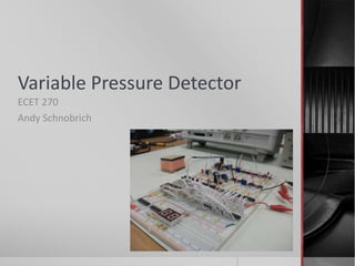


The document outlines the design of a variable pressure detector using a variable capacitor as a pressure switch, incorporating both analog and digital components for pressure detection and time display. It details various electronic circuits including a Wien bridge oscillator, active rectifiers, and a monostable multivibrator, alongside resistor and capacitor configurations necessary for operation. Additionally, it describes the integration of display and counting circuits to indicate pressure levels visually.


