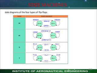
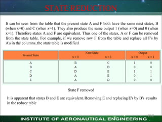
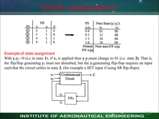
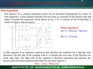
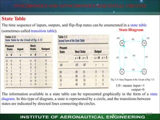
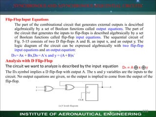
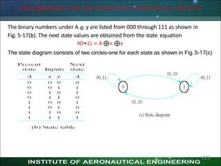
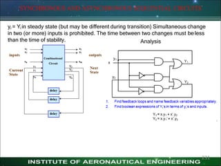
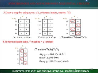
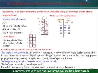
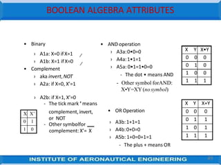
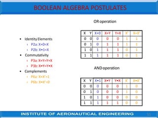
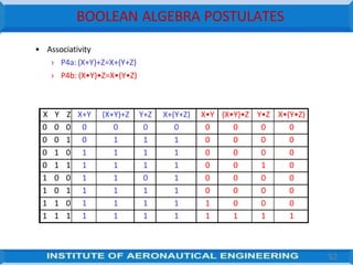
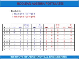
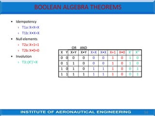
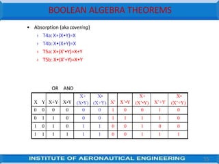
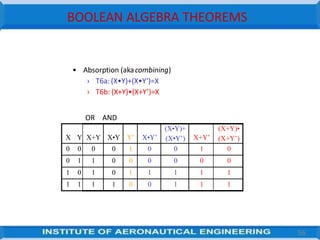
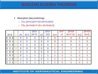
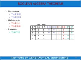
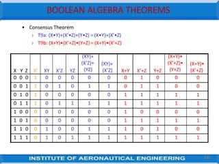
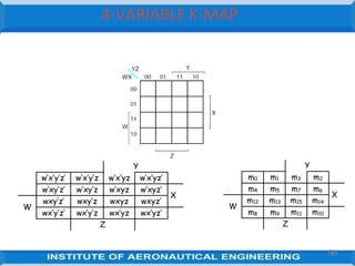
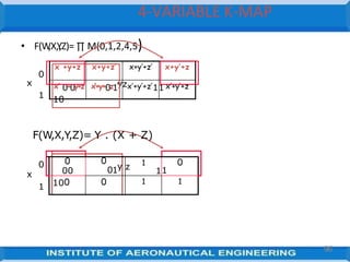
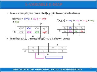
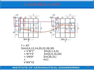
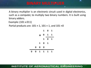
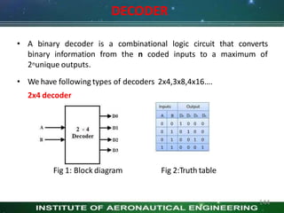
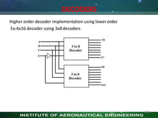
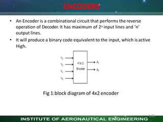
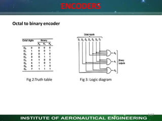
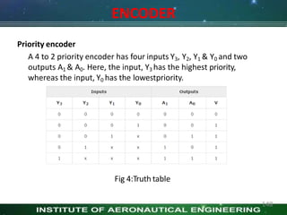
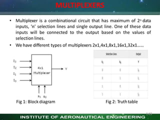
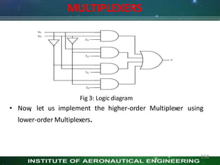
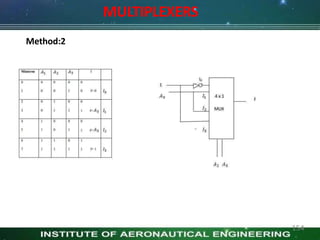
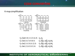
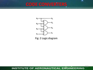
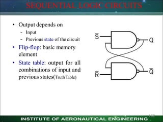
This document contains a presentation on digital logic design. It discusses topics like number systems, number base conversion, binary arithmetic operations, weighted and non-weighted binary codes, and binary coded decimal arithmetic. The presentation was created by faculty at the Institute of Aeronautical Engineering for computer science and information technology students as part of a course on digital logic design.


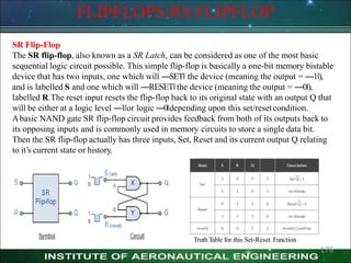


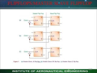
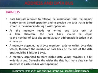
![FLIPFLOPS:MASTER SLAVE FLIPFLOP
MASTER SLAVE FLIPFLOP
Master-slave flip flop is designed using two separate flip flops. Out of these, one acts as
the master and the other as a slave. The figure of a master-slave J-K flip flop is shown
below.
From the above figure you can see that both the J-K flip flops are presented in a
series connection. The output of the master J-K flip flop is fed to the input of the slave
J-K flip flop. The output of the slave J-K flip flop is given as a feedback to the input of
the master J-K flip flop. The clock pulse [Clk] is given to the master J-K flip flop and it
is sent through a NOT Gate and thus inverted before passing it to the slave J-K flip
flop.
186](https://image.slidesharecdn.com/dldppt0-230720061112-46846e87/85/DLD_PPT_0-pptx-186-320.jpg)