Download to read offline
![Dr. D. Chinni Krishna. Int. Journal of Engineering Research and Application www.ijera.com
ISSN : 2248-9622, Vol. 7, Issue 2, ( Part -3) February 2017, pp.01-06
www.ijera.com DOI: 10.9790/9622- 0702030106 1 | P a g e
Displaying of Digital Clock through digital circuits and through
Assembly Language Programs of 8051 microcontroller
Dr. D. Chinni Krishna*
and U. Sridevi**
*Department of Physics, Bhavan’s New Science College, Narayanaguda, Hyderabad-500 029, Telangana State,
India.
**Department of Mathematics, Govt. City College, Nayapul, Hyderabad-500 001, Telangana State, India
ABSTRACT
With a view to display a Digital Clock through digital circuits using modulo-n (mod-n) counters, a
circuit diagram was designed and implemented it through multi simulation software. In the similar manner the
time digits were displayed on seven segment displays at 8255 programmable peripheral interface (PPI) ports
through 8051 microcontroller, the time digits (hours, minutes and seconds) were connected to the first 8255 PPI
and the date digits (Years, months and days) were connected to second 8255 PPI. The detailed circuit diagram
was given to understand the construction details of the circuit. The loop in a loop technique of assembly
language program was used to display date and time. After displaying a year, month and day on the date
displays through main program, it calls 1day subroutine to display time in 24 hours clock. The 1day subroutine
calls 1second delay subroutine to change the digits in seconds display. After completion of 24 hours time, the
digit will be changed in the days display to indicate the next date. After completion of 31 days in the first month,
the main program calls month subroutine to change the digit in the months display. Precautions were taken to
change the digits in months display for January 31 days, February 28 days, March 31 days, April 30 days, May
31 days, June 30 days, July 31 days, August 31 days, September 30 days, October 31 days, November 30 days
and December 31 days. After completion of a month, there will be a change in years digit and this process will
be repeated continuously.
Keywords: Digital Clock, Modulo-n Counters, Interfacing, Assembly Language program, Loop in Loop
technique, Binary Coded Decimal (BCD) number
I. INTRODUCTION
In the digital era, designing of a digital
clock and maintaining of its digits without any
error is one of the important tasks of the circuit
designer. The sequential circuits of digital
electronics were implemented to design the clock.
The modulo-n counters are used to give the
required data to display the digits of a digital clock
on 7 segment displays.
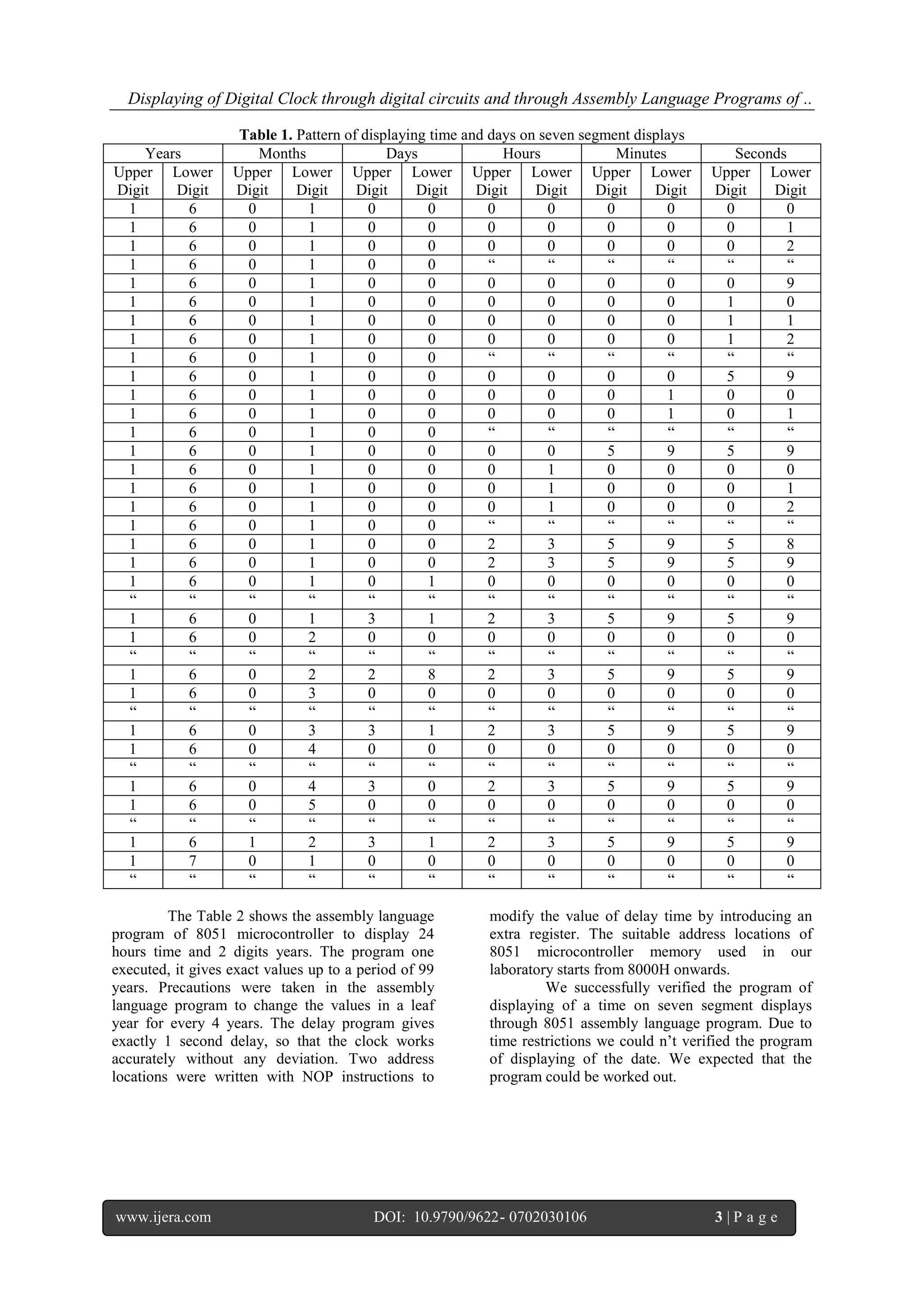
II. RESULTS AND DISCUSSIONS
The general circuit diagram of 24 hours Digital
Clock with digital circuits as given in a text book
[1] with clock input was designed by using mod-n
counters as shown in Fig. 1.
Fig. 1. Digital clock by using mod-n counter digital circuits
RESEARCH ARTICLE OPEN ACCESS](https://image.slidesharecdn.com/a0702030106-170221094615/75/Displaying-of-Digital-Clock-through-digital-circuits-and-through-Assembly-Language-Programs-of-8051-microcontroller-1-2048.jpg)
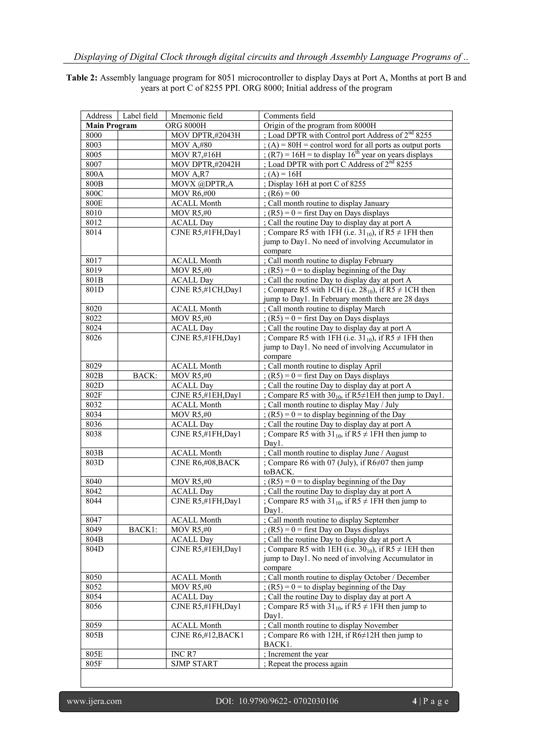
![Dr. D. Chinni Krishna. Int. Journal of Engineering Research and Application www.ijera.com
ISSN : 2248-9622, Vol. 7, Issue 2, ( Part -3) February 2017, pp.01-06
www.ijera.com DOI: 10.9790/9622- 0702030106 2 | P a g e
The practical circuit diagram to design a 24 hours
digital clock by using mod-n counters on Multi-
simulation software [2] with execution results were
shown in Fig. 2.
Fig. 2. The 24 hours digital clock
It is observed from figure 2 that, each digit
in LSB reaches its required value may apply a
clock pulse to its next higher digit. When the clock
pulse reached to minutes place, it clears all digits in
seconds place. Similarly, when a clock pulse
reached to hours place, then all digits in minutes
and seconds place will be cleared. When it reaches
highest value all digits were cleared and it repeated
in incrementing mode. Change the clock position to
set or reset any of the digits in a digital clock.
The experimental diagram to display Time
and date through 8051 microcontroller as its ports
information given in a text book [3] was given in
Fig. 3. One 8255 ports are used to control the Time
digits and another 8255 PPI ports are used to
control the digits of the date. The Table 1 shows
the 8255 ports bit conditions to display time and
date in a systematic manner.
Fig. 3. Displaying of Time and Date through 8051 microcontroller and 8255 PPI ports](https://image.slidesharecdn.com/a0702030106-170221094615/75/Displaying-of-Digital-Clock-through-digital-circuits-and-through-Assembly-Language-Programs-of-8051-microcontroller-2-2048.jpg)
![Displaying of Digital Clock through digital circuits and through Assembly Language Programs of ..
www.ijera.com DOI: 10.9790/9622- 0702030106 6 | P a g e
III. CONCLUSIONS
1. The modulo-n counters were used to generate a
digital clock
2. Change the clock position to set or reset any of
the digits in the digital clock.
3. The lower digits reaches its maximum value, it
supplies a clock pulse to its higher digit.
4. When higher digits are resetting, they clears all
its lower positions.
5. Two separate 8255 PPIs required to display
time and date separately
6. The delay subroutine must give exactly 1
second delay to display time and date
accurately.
7. It is cheapest to design the digital clock with
digital circuits than with the microprocessors.
ACKNOWLEDGEMENT
The first & corresponding author would
like to express thanks to Dr. S. Jaikishan garu, the
Chairman, Secretary & Correspondent of Bhavan’s
New Science College for encouraging him to carry
out the research work and publish papers. He also
thanks the management for providing the facilities
in Department of Physics to carry out the above
project. He also likes to wishes his thanks to his
colleagues Dr. P. Indira, Dr. S. Laxmi Srinivasa
Rao (The In charge Principal of BNSC (Day)), Sri.
D. Sambasiva Rao, Dr. B.V. Prasad, Dr. RVGK
Mohan, Dr. S. Jagan Mohan, Mr. B. Anjaiah, Ms.
Shahenn Sk, Mr. N. Venkateswar Reddy and Ms.
Asiya for their encouragement and support. He
would also like to express his thanks to Mr. Balraj,
Mr. Suresh, Mr. Sriram, the Non teaching staff of
Dept. of Physics of BNSC for their support.
He also wishes his thanks to his family
members and friends for their support. He would
like to convey his best wishes to his small kid
Master Krishna Chaithanya, who makes the author
in a refreshing mind by his smile and kidding
actions. Finally he would like to express his thanks
to his M.Sc. Applied Electronics students for their
support.
REFERENCES
[1] R.P. Jain and M.M.S. Anand; Digital
Electronics Practice using Integrated
Circuits, Tata McGraw-Hill Publishing
Company Limited, New Delhi.
[2] Dr. D. Chinni Krishna, Volume 3,
Number 2, Gaussian Journal of Science &
Applications, July-December 2015. ISSN:
2348-0440
[3] Muhammad Ali Mazidi, Jainice Gillispie
Mazidi and Rolin D. McKinlay; The 8051
Microcontrollers and Embedded Systems
using Assembly and C, Second Edition,
Eastern Economy Edition-2006, Prentice
Hall of India Private Limited, New Delhi-
110001.
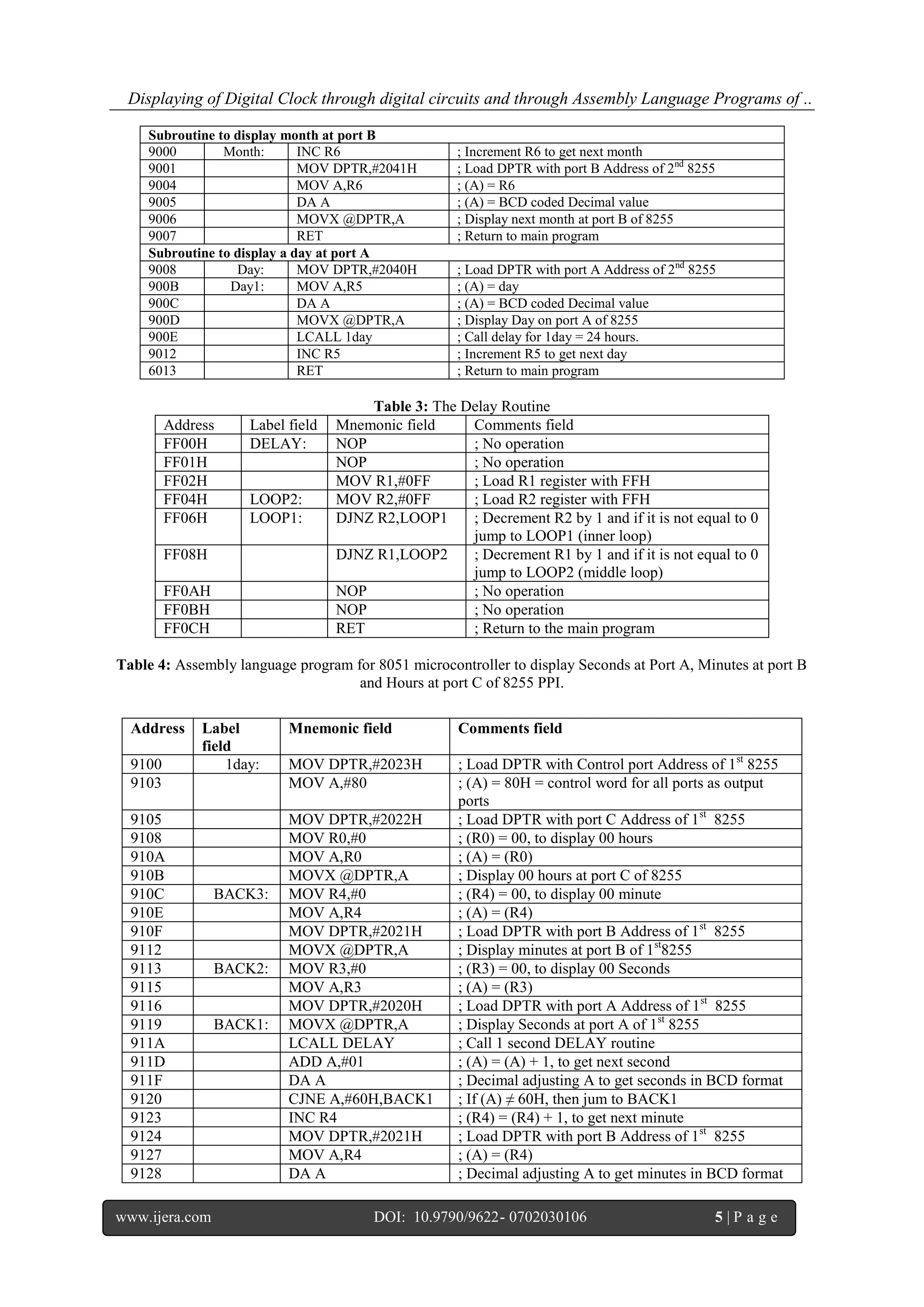
9129 MOVX @DPTR,A ; Display minutes at port B of 1st
8255
912A CJNE A,#60H,BACK2 ; If (A) ≠ 60H, then jump to BACK1
912D INC R0 ; (R0) = (R0) + 01, to get next hour
912E MOV A,R0 ; (A) = (R0)
912F DA A ; Decimal adjusting A to get hours in BCD format
9130 CJNE A,#24H,BACK2 ; If (A) ≠ 24H, then jump to BACK3
9133 RET ; Return to main program](https://image.slidesharecdn.com/a0702030106-170221094615/75/Displaying-of-Digital-Clock-through-digital-circuits-and-through-Assembly-Language-Programs-of-8051-microcontroller-6-2048.jpg)

This document presents the design and implementation of a digital clock using digital circuits and assembly language programs for the 8051 microcontroller. It details circuit diagrams, the use of modulo-n counters, and methods for interacting with 8255 programmable peripheral interface ports for displaying time and date. The assembly language program enables accurate display of time, incorporating subroutines for date management, including handling of varying month lengths.