Download to read offline
![41 International Journal for Modern Trends in Science and Technology
Volume: 2 | Issue: 08 | August 2016 | ISSN: 2455-3778IJMTST
Design and implementation of Closed
Loop Control of Three Phase Interleaved
PFC AC-DC Converter
K. Vasantha Lakshmi1
| P.C. Chakravarthy2
1PG Scholar, Department of Electrical & Electronics Engineering, Sarada Institute of Science
Technology & Management, Srikakulam (Dt), A.P, India.
2Associate Professor & Head, Department of Electrical & Electronics Engineering, Sarada Institute of
Science Technology & Management, Srikakulam (Dt), A.P, India.
A single-phase, three-level, single-stage power-factor corrected AC/DC converter operated under closed
loop manner is presented. That operates with a single controller to regulate the output voltage and the input
inductor act as a boost inductor to have a single stage power factor correction with good output response. The
paper deals with a new single stage three level ac-dc converter which performs both power factor correction
and voltage regulation in a single stage. The proposed converter has two separate controllers, one for power
factor correction and the other for regulating the output voltage. A comprehensive review of the existing single
stage topologies has been carried out. Then the operating principle, control scheme and the design of the new
converter are presented. The proposed converter is having an input power factor close to unity and better
voltage regulation compared to the conventional ac-dc converter topologies. Proposed topology is evaluated
through Matlab/Simulink platform and simulation results are conferred.
KEYWORDS: Power Factor Correction, Single Stage Converters, AC–DC Power Factor Correction, Three
Level Converters, Closed Loop Control Logic.
Copyright © 2016 International Journal for Modern Trends in Science and Technology
All rights reserved.
I. INTRODUCTION
Power-electronic converters are becoming
popular for various industrial drives applications.
In recent years also high-power and
medium-voltage drive applications have been
installed. To overcome the limited semiconductor
voltage and current ratings, some kind of series
and/or parallel connection will be necessary. Due
to their ability to synthesize waveforms with a
better harmonic spectrum and attain higher
voltages, multi-level inverters are receiving
increasing attention in the past few years. THE
ac–dc power supplies with transformer isolation
are typically implemented with some sort of input
power factor correction (PFC) to comply with
harmonic standards such as IEC 1000-3-2 [1]-[3].
Although it is possible to satisfy these standards by
adding passive filter elements to the traditional
passive diode rectifier/LC filter input combination,
the resulting converter would be very bulky and
heavy due to the size of the low-frequency
inductors and capacitors. The most common
approach to PFC is to use two-stage power
conversion schemes. These two-stage schemes use
a front-end ac–dc converter stage to perform ac–dc
conversion with PFC with the output of the
front-end converter fed to a back-end dc–dc
converter stage that produces the desired isolated
dc output voltage [4]. Using two converter stages in
this manner, however, increases the cost, size, and
complexity of the overall ac–dc converter, and this
has led to the emergence of single-stage
power-factor-corrected converters.
In order to reduce the cost, size, and complexity
associated with two-stage ac–dc power conversion
and PFC, researchers have tried to propose
single-stage converters that integrate the functions
of PFC and isolated dc–dc conversion in a single
power converter. Several single-phase [5]–[10] and
three-phase [4] converters have been proposed in
the literature, with three-phase converters being
preferred over single-phase converters for higher
power applications. Previously proposed
ABSTRACT](https://image.slidesharecdn.com/122ijmtst020845-160901161648/75/Design-and-implementation-of-Closed-Loop-Control-of-Three-Phase-Interleaved-PFC-AC-DC-Converter-1-2048.jpg)
![42 International Journal for Modern Trends in Science and Technology
Design and implementation of Closed Loop Control of Three Phase Interleaved PFC AC-DC Converter
three-phase single-stage ac–dc converters,
however, have at least one of the following
drawbacks that have limited their widespread use.
1) They are implemented with three separate ac–dc
single stage modules
2) The converter components are exposed to very
high dc bus voltages so that switches and bulk
capacitors with very high voltage ratings are
required.
3) The input currents are distorted and contain a
significant amount of low-frequency harmonics
because the converter has difficulty performing
PFC and dc–dc conversion simultaneously.
4) The converter must be controlled using very
sophisticated techniques and/or nonstandard
techniques [5]–[11]. This is particularly true for
resonant-type converters that need
variable-switching-frequency control methods to
operate.
5) The output inductance must be very low, which
makes the output current to be discontinuous.
This results in a very high output ripple so that
secondary diodes with high peak current ratings
and large output capacitors to filter the ripple are
needed.
6) Most of them are in discontinuous conduction
mode at the input and need to have a large input
filter to filter out large high-frequency harmonics
[4].
II. THE SINGLE STAGE POWER FACTOR CORRECTED
TOPOLOGIES
One classification of the SSPFC circuits is based
on the number of switches in the converter. The
SSPFC circuits provide the features of the power
factor pre-regulators in addition to those of dc-dc
converters cascaded with it. The basic SSPFC
circuit was introduced in early 1990s by Madigan.
This was achieved by integrating the boost input
shaping converter with either a fly-back or a
forward topology.
A. Single switch topologies:
Many single switch single stage converter
topologies have been proposed. A single stage ac-dc
converter is proposed in which the dc voltage is less
dependent on the operating conditions. But the
voltage stress is more on the switch. Also it
contains low frequency output voltage ripples. The
various problems associated with single switch
topologies are lower power factor at low line input,
dead angle problem of input current high capacitor
voltage stress and higher switch voltage.
B. Two switch topologies:
Half bridge converters have also been integrated
in SSPFC topologies either in symmetrical or
asymmetrical modes of operation. They are able to
provide high input power factor. Still they suffer
from high circulating currents, high dc bus
voltages or discontinuous currents.
Fig.1 proposed three level single stage converters
The topology proposed in has an auxiliary circuit
which is used to get a reduced capacitor voltage
stress. Here the converter is operated in DCM, thus
achieving high input power factor. But the current
stress on the converter switches becomes high.
Thus the conduction losses increase resulting in
lower efficiency. Hence these converters cannot be
used for higher power applications.
Fig.1 shows a new three level single stage
converter which eliminates the limitations of the
previous topologies. It consists of a boost converter
section and an isolated forward converter section.
The authors proposed a three-phase single-stage
three-level converter to mitigate these drawbacks.
Although the converter proposed in that paper was
an advance over previously proposed three-phase
single-stage converters, it still suffered from the
need to have a discontinuous output inductor
current at light-load conditions to keep the dc bus
capacitor voltage<450 V, and it needed to operate
with discontinuous input current, which resulted
in high component current stress and the need for
significant input filtering due to the large amount
of ripple.
This paper presents a new interleaved
three-phase single stage rectifier that does not
have any of these drawbacks. The work presented
in this paper can be considered to be a follow-up
work in relation to what was presented. In
comparison to the converter presented, the
converter presented in this paper has an
interleaved structure, requires two fewer diodes in
the dc bus, has an output current which is
continuous for all load ranges, has a dc bus voltage
that is less than 450 V for all load conditions, and](https://image.slidesharecdn.com/122ijmtst020845-160901161648/75/Design-and-implementation-of-Closed-Loop-Control-of-Three-Phase-Interleaved-PFC-AC-DC-Converter-2-2048.jpg)
![43 International Journal for Modern Trends in Science and Technology
Volume: 2 | Issue: 08 | August 2016 | ISSN: 2455-3778IJMTST
has a much better input current harmonic content.
In this paper, the operation of the new converter is
explained; its features and design are discussed.
Fig.2 Proposed interleaved three-phase three-level
converter
Several SSPFC topologies have been introduced
so far by various power electronic researchers. In
the next section a review of the various SSPFC
topologies is been carried out.
III. PROPOSED CONVERTER OPERATION
The proposed converter and its key waveforms
are shown in Figs. 2 and 3, respectively. The
proposed converter uses auxiliary windings that
are taken from the converter transformer to act as
―magnetic switches‖ to cancel the dc bus capacitor
voltage so that the voltage that appears across the
diode bridge output is zero. When the primary
voltage of the main transformer is positive,
auxiliary winding 1 (Naux1/N1=2) cancels out the
dc bus voltage so that the output voltage of diode
bridge 1(DB1) is zero and the currents in input
inductors La1, Lb1, and Lc1 rise. When the
primary voltage of the main transformer is
negative, auxiliary winding 2 (Naux2/N1=2)
cancels out the dc bus voltage so that the output
voltage of diode bridge 2(DB2) is zero and the
currents in input inductors La2, Lb2, and Lc2 rise.
When there is no voltage across the main
transformer primary winding, the total voltage
across the dc bus capacitors appears at the output
of the diode bridges and the input currents fall
since this voltage is greater than the input voltage.
If the input currents are discontinuous, the
envelope of the input current will be sinusoidal and
in phase with the input voltages. The converter
modes of operation are explained in this section.
The typical converter waveforms are shown in Fig.
3. The equivalent circuit in each stage is shown in
Fig. 4. The converter goes through the following
modes of operation.
Mode 1(t0<t<t1)[Fig. 4(a)]: During this interval,
switches S1andS2are ON. In this mode, the energy
from dc bus capacitorC1 flows to the output load.
Due to magnetic coupling, a voltage appears across
auxiliary winding 1 which is equal to the dc bus
voltage but has opposite polarity and cancels the
total dc bus capacitor voltage; the voltage at the
diode bridge output is zero, and the input currents
inLa1,Lb1, andLc1rise.
Mode 2(t1<t<t2) [Fig. 4(b)]: In this mode, S1 is OFF,
and S2 remains ON. The energy stored in
L1(L1=Labc1) during the previous mode starts to
transfer into the dc bus capacitors. The voltage
that appears across auxiliary winding 1 is zero. The
primary current of the main transformer circulates
throughD1 andS2. With respect to the converter’s
output section, the load inductor current
freewheels in the secondary of the transformer,
which defines a voltage across the load filter
inductor equal to−VL.
Mode 3(t2<t<t3)[Fig. 4(c)]: In this mode,S1 and S2
are OFF. The energy stored inL1still is transferring
into the dc bus capacitor. The primary current of
the transformer charges C2 through the body
diodes of S3and S4. Switches S3andS4are
switched ON at the end of this mode.
Mode 4(t3<t<t4) [Fig. 4(d)]: In this mode, S3 andS4
are ON, and the energy flows from capacitor C2
into the load. The voltage appears across auxiliary
winding 2 which is equal to the dc bus voltage but
acts like a magnetic switch and cancels out the dc
bus voltage. The voltage across the boost inductors
L2(L2=Labc2)becomes only the rectified supply
voltage of each phase, and the current flowing
through each inductor increases. This mode ends
when the energy stored inL1completely transfers
into the dc bus capacitor. For the remainder of the
switching cycle, the converter goes through modes
1–4 but with S3andS4 ON instead ofS1andS2and
with DB2instead of DB1.
Fig.3 Typical waveforms describing the modes of operation](https://image.slidesharecdn.com/122ijmtst020845-160901161648/75/Design-and-implementation-of-Closed-Loop-Control-of-Three-Phase-Interleaved-PFC-AC-DC-Converter-3-2048.jpg)
![44 International Journal for Modern Trends in Science and Technology
Design and implementation of Closed Loop Control of Three Phase Interleaved PFC AC-DC Converter
Fig. 4. Modes of operation. (a) Mode 1(t0<t<t1). (b) Mode 2
(t1<t<t2). (c) Mode 3 (t2<t<t3). (d) Mode 4 (t3<t<t4). (e) Mode
5 (t4<t<t5). (f) Mode 6(t5<t<t6). (g) Mode 7(t6<t<t7). (h) Mode
8(t7<t<t8)
Mode 5(t4<t<t5)[Fig. 4(e)]: In this mode,S3 and S4
are ON, and a symmetrical period begins. In this
mode, the energy flows from capacitor C2 into the
load. The voltage across the boost inductors L2
becomes only the rectified supply voltage of each
phase, and the current flowing through each
inductor increases.
Mode 6(t5<t<t6)[Fig. 4(f)]: In this mode,S3 is ON
and S4 is OFF, and the primary current of the main
transformer circulates through diodeD2 andS3.
The energy stored in the boost inductors L2during
the previous mode starts transferring into the dc
bus capacitor. The output inductor current also
freewheels in the secondary of the transformer
during this mode.
Mode 7(t6<t<t7)[Fig. 4(g)]: In this
mode,S3andS4are
OFF, and the primary current of the transformer
charges capacitorC1through the body diodes of
S1andS2.The energy stored in the boost
inductorsL2transfers into the dc bus capacitor.
Mode 8(t7<t<t8)[Fig. 4(h)]: In this mode,S1and
S2are ON. In this mode, the energy from dc bus
capacitor C1 flows to the output load. This mode
ends when the energy in the inductors L2
completely transfers into the dc bus capacitors.
Time t8 is the end of the switching cycle, and
another switching cycle begins with the same
modes
It should be noted that the input current is the
summation of inductor currentsiL1andiL2which
are both discontinuous. However, by selecting
appropriate values for L1 (=La1=Lb1=Lc1) and
L2(=La2=Lb2=Lc2) in such a way that two inductor
currents such as iLa1andiLa2have to overlap each](https://image.slidesharecdn.com/122ijmtst020845-160901161648/75/Design-and-implementation-of-Closed-Loop-Control-of-Three-Phase-Interleaved-PFC-AC-DC-Converter-4-2048.jpg)
![46 International Journal for Modern Trends in Science and Technology
Design and implementation of Closed Loop Control of Three Phase Interleaved PFC AC-DC Converter
Case 2: Design of Closed -Loop Circuit of Proposed AC-DC
Converter:
Fig.11. Matlab/Simulink Model of Proposed Converter
Operated under Closed Loop Manner
Fig.12.
Output Voltage & Current of Proposed Converter Operated
under Closed Loop Manner
Fig.13. Simulated input wave form of the Voltage and
current of the closed loop of proposed converter.
Fig.13. Source Side Voltage & Current – in Phase
Condition, depicts the unity power factor at source
side, with low THD response and maintain
qualities power at utility side, as per IE standards
VI. CONCLUSION
Numerous industrial applications have begun to
require higher power apparatus in recent years.
Power-electronic converters are becoming popular
for various industrial applications. In this concept
a new three level AC to DC converter for closed loop
control logic for updating the performance of the dc
drive and also a new three-phase three-level
single-stage power-factor corrected ac–dc converter
with interleaved input has been proposed in this
paper. The converter operates with a single
controller to regulate the output voltage and uses
auxiliary windings taken from its power
transformer as magnetic switches to cancel the dc
bus voltage so that the input section operates like a
boost converter. The proposed converter can
operate with input current harmonic content that
meets the IEC1000-3-2 standard. The converter
can operate with lower peak voltage stresses across
the switches and the DC bus capacitors as it is a
three-level converter. This converter provides
variable output voltage with improved power factor.
The all simulation results are verified through
Matlab/simulink software.
REFERENCES
[1] Limits for Harmonic Current Emission (Equipment
Input Current>16 Aper Phase), IEC1000-3-2 Int.
Std., 1995.
[2] Limits for Harmonic Current Emission (Equipment
Input Current>16 Aper Phase), IEC1000-3-4 Int.
Std., 1998.
[3] IEEE Recommended Practices and Requirements for
Harmonic Control in Electric Power Systems, IEEE
Std. 519-1992, Apr. 1993.
[4] B. Tamyurek and D. A. Torrey, ―A three-phase unity
power factor single stage AC–DC converter based on
an interleaved fly back topology, ‖IEEE Trans. Power
Electron., vol. 26, no. 1, pp. 308–318, Jan. 2011.
[5] J. M. Kwon, W. Y. Choi, and B. H. Kwon,
―Single-stage quasi-resonant fly back converter for a
cost-effective PDP sustain power module, ‖IEEE
Trans. Ind. Electron., vol. 58, no. 6, pp. 2372–2377,
Jun. 2011.
[6] H. L. Cheng, Y. C. Hsieh, and C. S. Lin, ―A novel
single-stage high-power factor AC/DC converter
featuring high circuit efficiency,‖ IEEE Trans. Ind.
Electron., vol. 58, no. 2, pp. 524–532, Feb. 2011.
[7] S. K. Ki and D. D.-C. Lu, ―Implementation of an
efficient transformer-less single-stage single-switch
AC/DC converter, ‖IEEE Trans. Ind. Electron., vol.
57, no. 12, pp. 4095–4105, Dec. 2010.
[8] H. Ma, Y. Ji, and Y. Xu, ―Design and analysis of
single-stage power factor correction converter with a
feedback winding, ‖IEEE Trans. Power Electron., vol.
25, no. 6, pp. 1460–1470, Jun. 2010.
[9] H. J. Chiu, Y. K. Lo, H. C. Lee, S. J. Cheng, Y. C. Yan,
C. Y. Lin, T. H. Wang, and S. C. Mou, ―A single-stage
soft-switching fly back converter for
power-factor-correction applications ,‖IEEE Trans.
Ind. Electron., vol. 57, no. 6, pp. 2187–2190, Jun.
2010.
[10]J. Zhang, D. D.-C. Lu, and T. Sun, ―Fly back-based
single-stage power factor-correction scheme with
time-multiplexing control,‖ IEEE Trans. Ind.
Electron., vol. 57, no. 3, pp. 1041–1049, March](https://image.slidesharecdn.com/122ijmtst020845-160901161648/75/Design-and-implementation-of-Closed-Loop-Control-of-Three-Phase-Interleaved-PFC-AC-DC-Converter-6-2048.jpg)

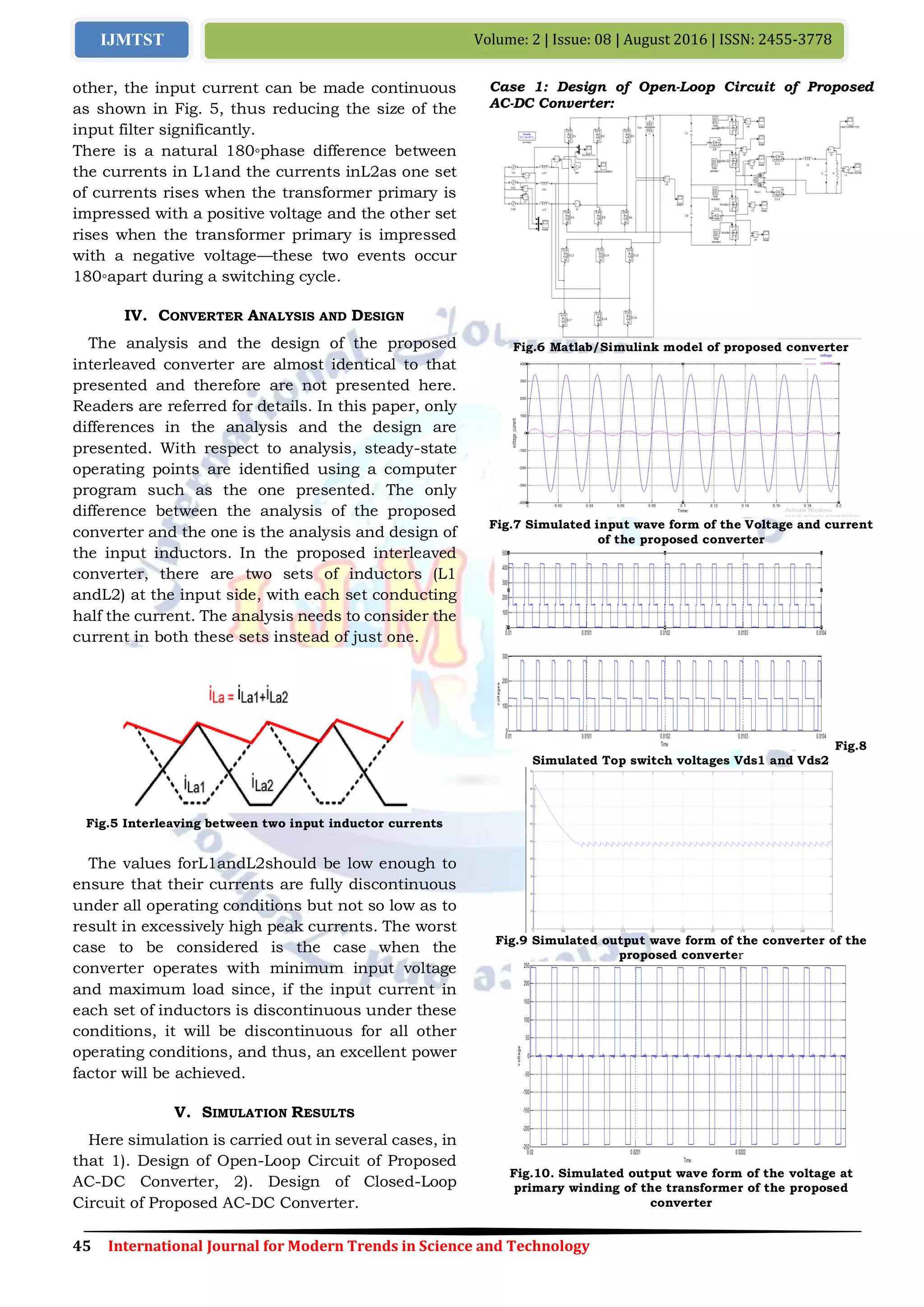
The document presents the design and implementation of a closed-loop control system for a three-phase interleaved power-factor-corrected (PFC) AC-DC converter. It introduces a new single-stage three-level converter that improves upon existing designs by achieving high input power factor and better voltage regulation while eliminating issues like high peak currents and the need for sophisticated control techniques. Simulation results demonstrate the effectiveness of the proposed converter, revealing continuous output current and improved harmonic content compared to traditional methodologies.


![[IJET V2I5P8] Authors: Lakshmi K R, Kavitha Issac, Kiran Boby](https://cdn.slidesharecdn.com/ss_thumbnails/ijet-v2i5p8-161107140749-thumbnail.jpg?width=640&height=640&fit=bounds)


![[IJET- V2I2P17] Authors: Gaurav B. Patil., Paresh J. Shah](https://cdn.slidesharecdn.com/ss_thumbnails/ijet-v2i2p17-160609042055-thumbnail.jpg?width=640&height=640&fit=bounds)


