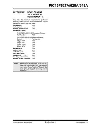
The document describes the PIC16F627A/628A/648A family of 8-bit microcontrollers. It includes a table comparing the features of devices in the family, such as available memory sizes and timers. The microcontrollers have integrated features to reduce external components and power consumption. Development support includes an assembler, simulator, emulator, and programmer.


![PIC16F627A/628A/648A
DS40044A-page 58 Preliminary 2002 Microchip Technology Inc.
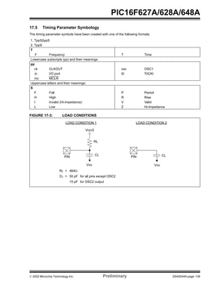
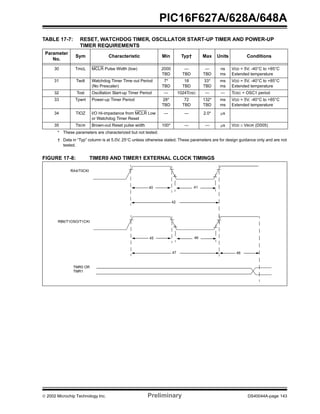
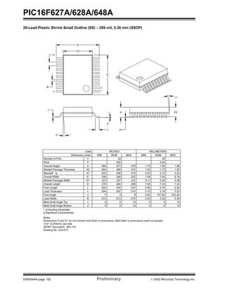
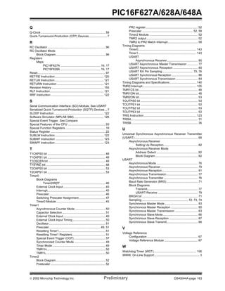
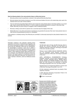
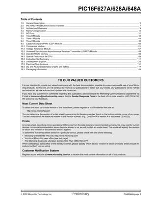
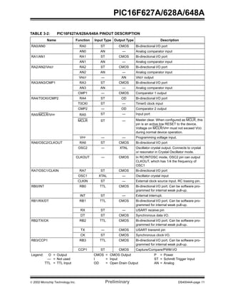
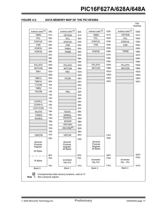
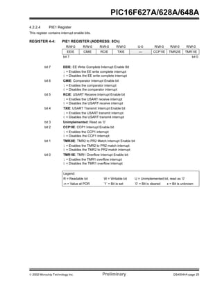
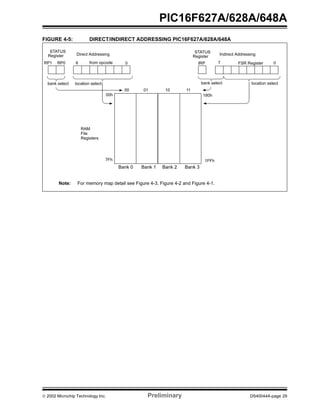
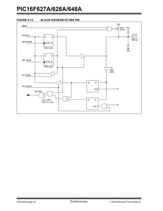
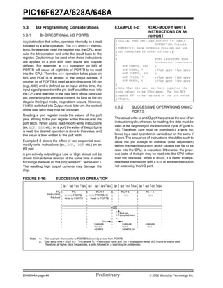
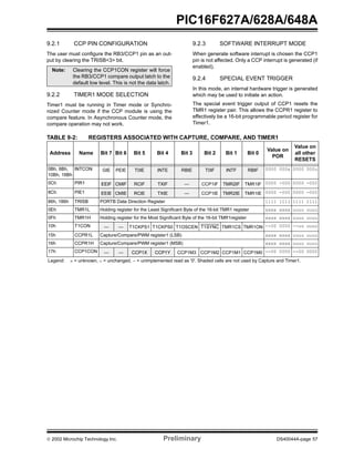
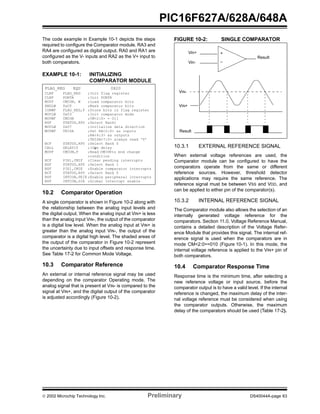
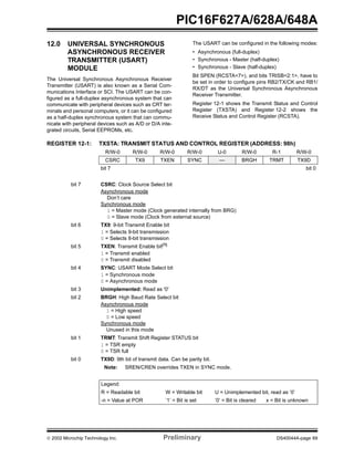
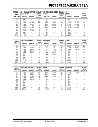
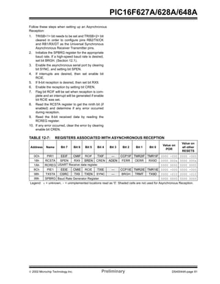
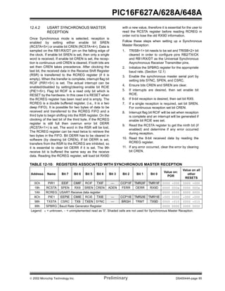
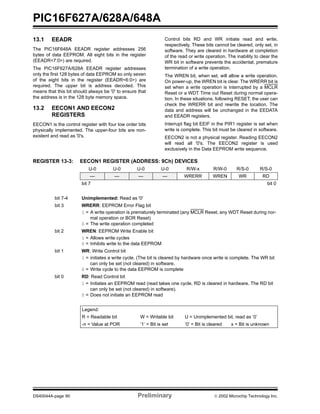
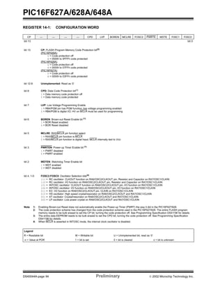
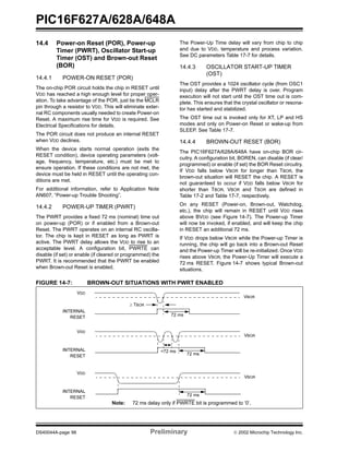
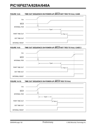
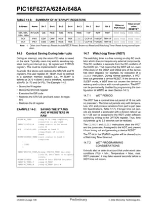
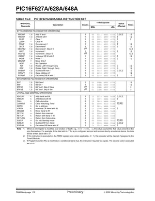
9.3 PWM Mode
In Pulse Width Modulation (PWM) mode, the CCP1 pin
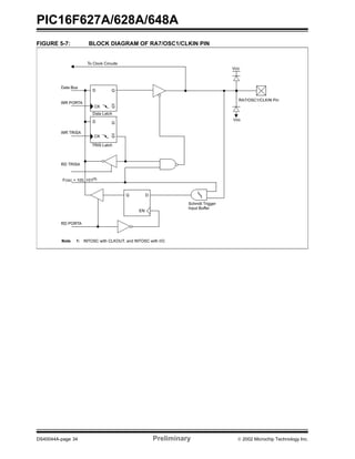
produces up to a 10-bit resolution PWM output. Since
the CCP1 pin is multiplexed with the PORTB data latch,
the TRISB<3> bit must be cleared to make the CCP1
pin an output.
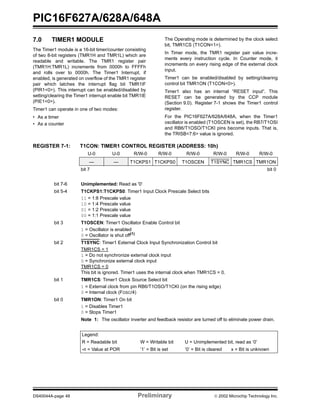
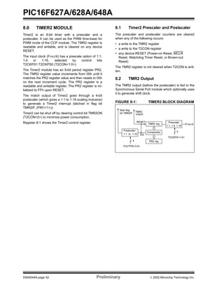
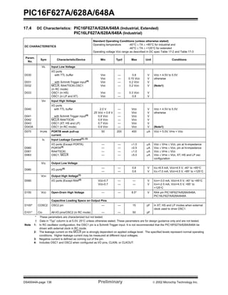
Figure 9-3 shows a simplified block diagram of the
CCP module in PWM mode.
For a step by step procedure on how to set up the CCP
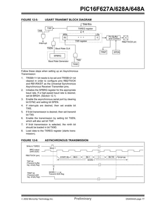
module for PWM operation, see Section 9.3.3.
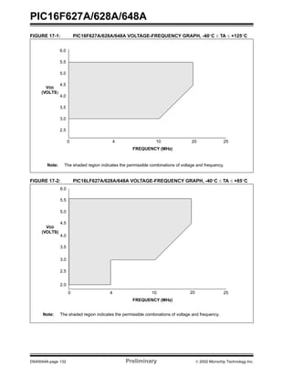
FIGURE 9-3: SIMPLIFIED PWM BLOCK
DIAGRAM
A PWM output (Figure 9-4) has a time base (period)
and a time that the output stays high (duty cycle). The
frequency of the PWM is the inverse of the period (fre-
quency = 1/period).
FIGURE 9-4: PWM OUTPUT
9.3.1 PWM PERIOD
The PWM period is specified by writing to the PR2 reg-
ister. The PWM period can be calculated using the fol-
lowing formula:
PWM frequency is defined as 1 / [PWM period].
When TMR2 is equal to PR2, the following three events
occur on the next increment cycle:
• TMR2 is cleared
• The CCP1 pin is set (exception: if PWM duty
cycle = 0%, the CCP1 pin will not be set)
• The PWM duty cycle is latched from CCPR1L into
CCPR1H
Note: Clearing the CCP1CON register will force
the CCP1 PWM output latch to the default
low level. This is not the PORTB I/O data
latch.
CCPR1L
CCPR1H (Slave)
Comparator
TMR2
Comparator
PR2
(1)
R Q
S
Duty cycle registers CCP1CON<5:4>
Clear Timer,
CCP1 pin and
latch D.C.
TRISB<3>
RB3/CCP1
Note 1: 8-bit timer is concatenated with 2-bit internal Q
clock or 2 bits of the prescaler to create 10-bit
time-base.
Note: The Timer2 postscaler (see Section 8.0) is
not used in the determination of the PWM
frequency. The postscaler could be used to
have a servo update rate at a different fre-
quency than the PWM output.
Period
Duty Cycle
TMR2 = PR2
TMR2 = Duty Cycle
TMR2 = PR2
PWM period PR2( ) 1+[ ] 4⋅ ⋅= Tosc TMR2 prescale⋅
value](https://image.slidesharecdn.com/datasheet-151201210636-lva1-app6891/85/Datasheet-60-320.jpg)


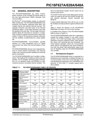
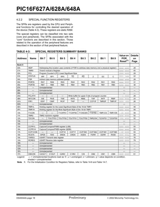
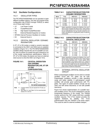
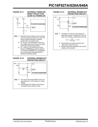
![ 2002 Microchip Technology Inc. Preliminary DS40044A-page 67
PIC16F627A/628A/648A
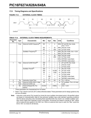
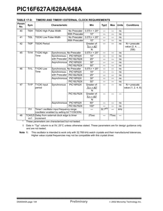
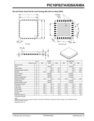
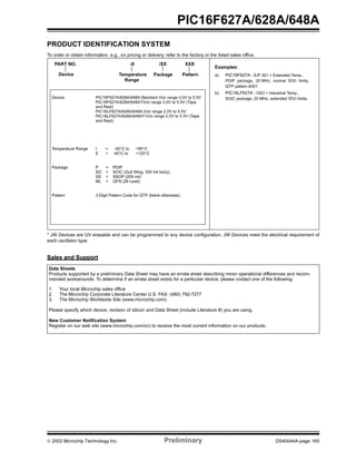
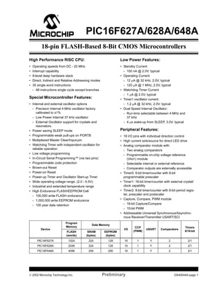
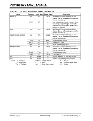
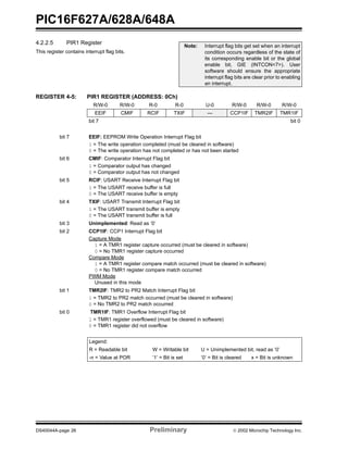
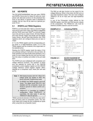
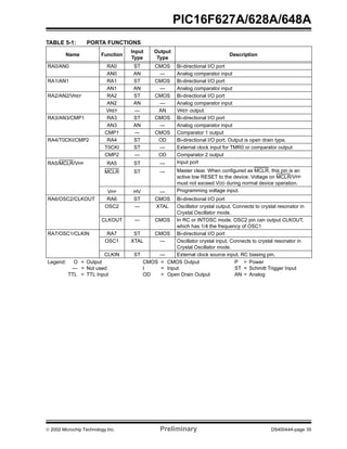
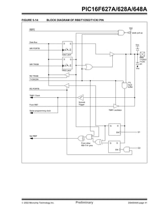
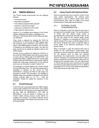
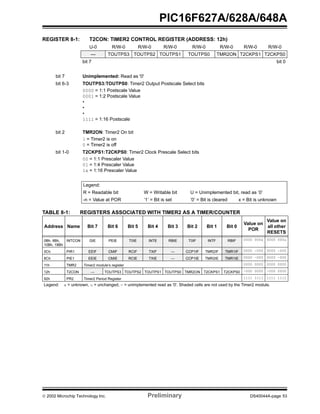
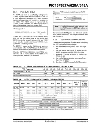
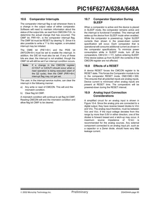
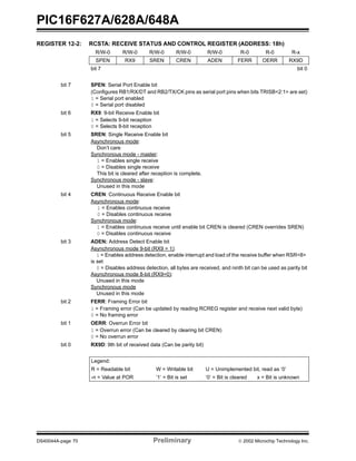
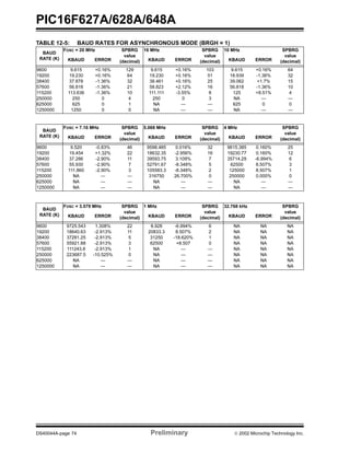
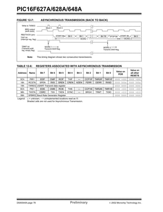
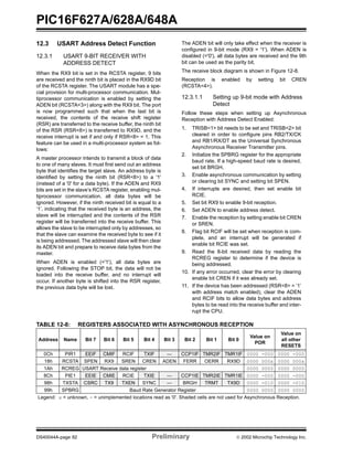
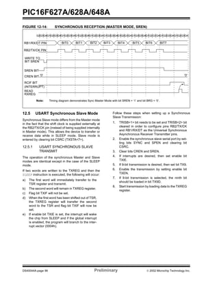
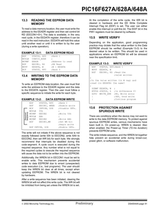
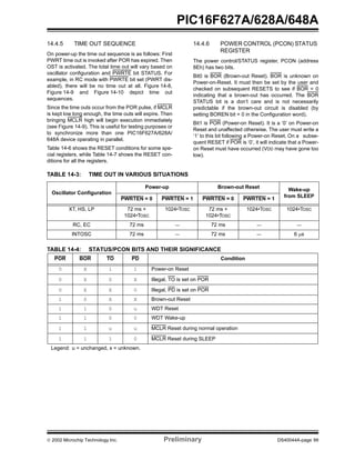
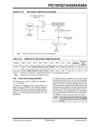
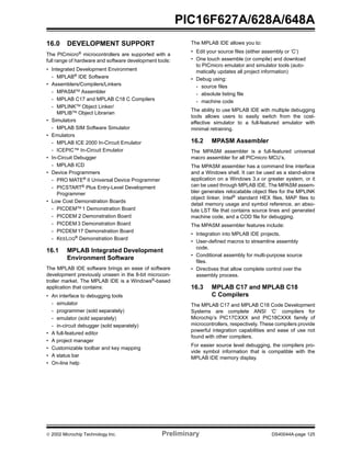
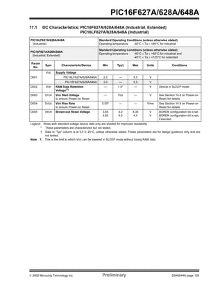
11.0 VOLTAGE REFERENCE
MODULE
The Voltage Reference is a 16-tap resistor ladder
network that provides a selectable voltage reference.
The resistor ladder is segmented to provide two ranges
of VREF values and has a power-down function to
conserve power when the reference is not being used.
The VRCON register controls the operation of the
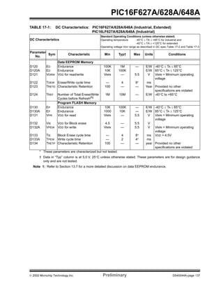
reference as shown in Figure 11-1. The block diagram
is given in Figure 11-1.
11.1 Voltage Reference Configuration
The Voltage Reference can output 16 distinct voltage
levels for each range.
The equations used to calculate the output of the
Voltage Reference are as follows:
if VRR = 1:
if VRR = 0:
The setting time of the Voltage Reference must be
considered when changing the VREF output
(Table 17-3). Example 11-1 demonstrates how Voltage
Reference is configured for an output voltage of 1.25V
with VDD = 5.0V.
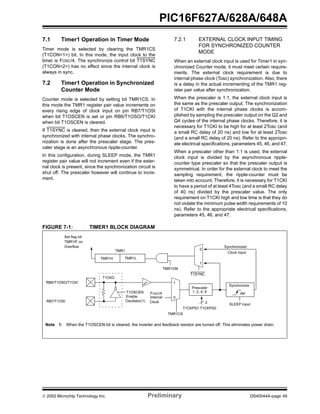
REGISTER 11-1: VRCON REGISTER (ADDRESS: 9Fh)
FIGURE 11-1: VOLTAGE REFERENCE BLOCK DIAGRAM
VREF
VR<3:0>
24
---------------------- VDD×=
VREF VDD
1
4
---×
VR<3:0>
32
----------------------+ VDD×=
R/W-0 R/W-0 R/W-0 U-0 R/W-0 R/W-0 R/W-0 R/W-0
VREN VROE VRR — VR3 VR2 VR1 VR0
bit 7 bit 0
bit 7 VREN: VREF Enable
1 = VREF circuit powered on
0 = VREF circuit powered down, no IDD drain
bit 6 VROE: VREF Output Enable
1 = VREF is output on RA2 pin
0 = VREF is disconnected from RA2 pin
bit 5 VRR: VREF Range selection
1 = Low Range
0 = High Range
bit 4 Unimplemented: Read as '0'
bit 3-0 VR<3:0>: VREF value selection 0 ≤ VR [3:0] ≤ 15
When VRR = 1: VREF = (VR<3:0>/ 24) * VDD
When VRR = 0: VREF = 1/4 * VDD + (VR<3:0>/ 32) * VDD
Legend:
R = Readable bit W = Writable bit U = Unimplemented bit, read as ‘0’
-n = Value at POR ’1’ = Bit is set ’0’ = Bit is cleared x = Bit is unknown
Note: R is defined in Table 17-3.
VRR8R
VR3
VR0
(From VRCON<3:0>)16-1 Analog Mux
8R R R R R
VREN
VREF
16 StagesVDD
VSS VSS](https://image.slidesharecdn.com/datasheet-151201210636-lva1-app6891/85/Datasheet-69-320.jpg)


![ 2002 Microchip Technology Inc. Preliminary DS40044A-page 111
PIC16F627A/628A/648A
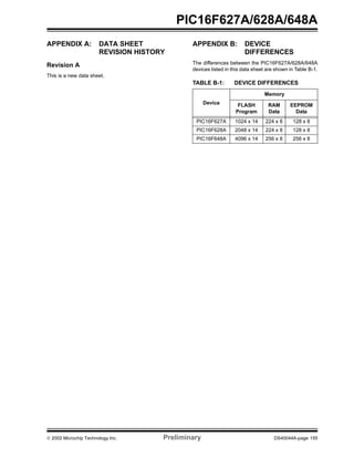
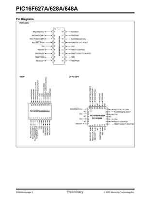
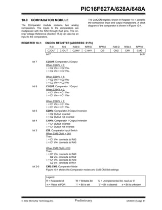
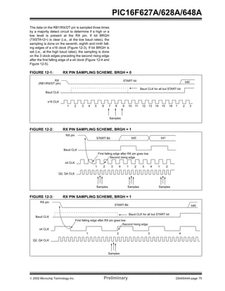
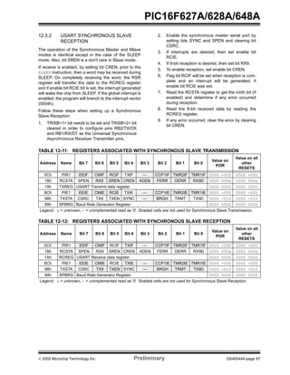
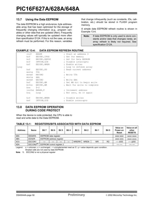
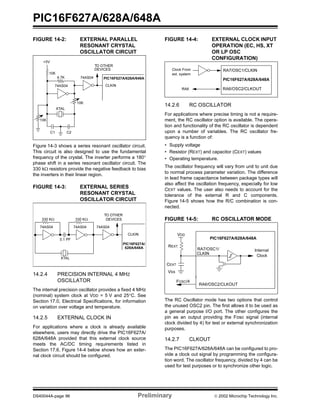
15.0 INSTRUCTION SET SUMMARY
Each PIC16F627A/628A/648A instruction is a 14-bit
word divided into an OPCODE which specifies the
instruction type and one or more operands which fur-
ther specify the operation of the instruction. The
PIC16F627A/628A/648A instruction set summary in
Table 15-2 lists byte-oriented, bit-oriented, and lit-
eral and control operations. Table 15-1 shows the
opcode field descriptions.
For byte-oriented instructions, 'f' represents a file
register designator and 'd' represents a destination
designator. The file register designator specifies which
file register is to be used by the instruction.
The destination designator specifies where the result of
the operation is to be placed. If 'd' is zero, the result is
placed in the W register. If 'd' is one, the result is placed
in the file register specified in the instruction.
For bit-oriented instructions, 'b' represents a bit field
designator which selects the number of the bit affected
by the operation, while 'f' represents the number of the
file in which the bit is located.
For literal and control operations, 'k' represents an
eight or eleven bit constant or literal value.
TABLE 15-1: OPCODE FIELD
DESCRIPTIONS
The instruction set is highly orthogonal and is grouped
into three basic categories:
• Byte-oriented operations
• Bit-oriented operations
• Literal and control operations
All instructions are executed within one single
instruction cycle, unless a conditional test is true or the
program counter is changed as a result of an
instruction. In this case, the execution takes two
instruction cycles with the second cycle executed as a
NOP. One instruction cycle consists of four oscillator
periods. Thus, for an oscillator frequency of 4 MHz, the
normal instruction execution time is 1 µs. If a
conditional test is true or the program counter is
changed as a result of an instruction, the instruction
execution time is 2 µs.
Table 15-2 lists the instructions recognized by the
MPASM™ assembler.
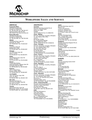
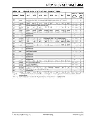
Figure 15-1 shows the three general formats that the
instructions can have.
All examples use the following format to represent a
hexadecimal number:
0xhh
where h signifies a hexadecimal digit.
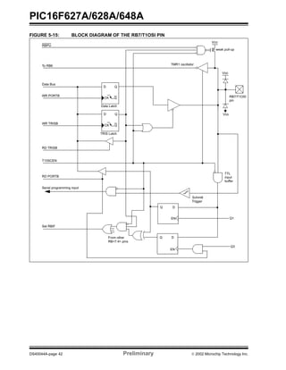
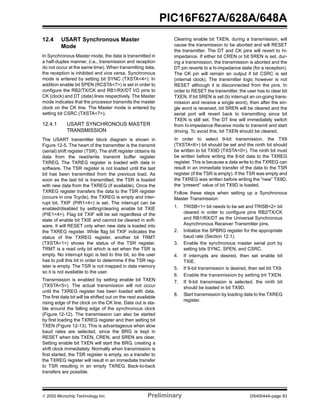
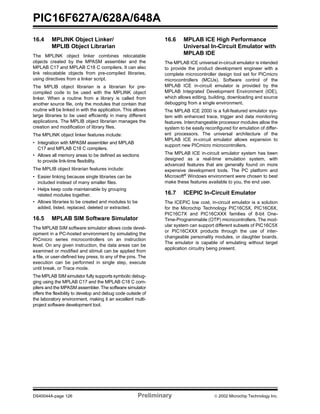
FIGURE 15-1: GENERAL FORMAT FOR
INSTRUCTIONS
Field Description
f Register file address (0x00 to 0x7F)
W Working register (accumulator)
b Bit address within an 8-bit file register
k Literal field, constant data or label
x Don't care location (= 0 or 1)
The assembler will generate code with x = 0. It is the
recommended form of use for compatibility with all
Microchip software tools.
d Destination select; d = 0: store result in W,
d = 1: store result in file register f.
Default is d = 1
label Label name
TOS Top of Stack
PC Program Counter
PCLATH Program Counter High Latch
GIE Global Interrupt Enable bit
WDT Watchdog Timer/Counter
TO Time out bit
PD Power-down bit
dest Destination either the W register or the specified regis-
ter file location
[ ] Options
( ) Contents
→ Assigned to
< > Register bit field
∈ In the set of
italics User defined term (font is courier)
Note 1: Any unused opcode is reserved. Use of
any reserved opcode may cause unex-
pected operation.
2: To maintain upward compatibility with
future PICmicro products, do not use the
OPTION and TRIS instructions.
Byte-oriented file register operations
d = 0 for destination W
OPCODE d f (FILE #)
d = 1 for destination f
f = 7-bit file register address
Bit-oriented file register operations
OPCODE b (BIT #) f (FILE #)
b = 3-bit bit address
f = 7-bit file register address
Literal and control operations
OPCODE k (literal)
k = 8-bit immediate value
OPCODE k (literal)
k = 11-bit immediate value
General
CALL and GOTO instructions only
13 8 7 6 0
13 10 9 7 06
13 8 7 0
13 11 10 0](https://image.slidesharecdn.com/datasheet-151201210636-lva1-app6891/85/Datasheet-113-320.jpg)
![ 2002 Microchip Technology Inc. Preliminary DS40044A-page 113
PIC16F627A/628A/648A
15.1 Instruction Descriptions
ADDLW Add Literal and W
Syntax: [ label ] ADDLW k
Operands: 0 ≤ k ≤ 255
Operation: (W) + k → (W)
Status Affected: C, DC, Z
Encoding: 11 111x kkkk kkkk
Description: The contents of the W register are
added to the eight bit literal 'k' and
the result is placed in the W register.
Words: 1
Cycles: 1
Example ADDLW 0x15
Before Instruction
W = 0x10
After Instruction
W = 0x25
ADDWF Add W and f
Syntax: [ label ] ADDWF f,d
Operands: 0 ≤ f ≤ 127
d ∈ [0,1]
Operation: (W) + (f) → (dest)
Status Affected: C, DC, Z
Encoding: 00 0111 dfff ffff
Description: Add the contents of the W register
with register 'f'. If 'd' is 0 the result is
stored in the W register. If 'd' is 1 the
result is stored back in register 'f'.
Words: 1
Cycles: 1
Example ADDWF REG1, 0
Before Instruction
W = 0x17
REG1 = 0xC2
After Instruction
W = 0xD9
REG1 = 0xC2
Z = 0
C = 0
DC = 0
ANDLW AND Literal with W
Syntax: [ label ] ANDLW k
Operands: 0 ≤ k ≤ 255
Operation: (W) .AND. (k) → (W)
Status Affected: Z
Encoding: 11 1001 kkkk kkkk
Description: The contents of W register are
AND’ed with the eight bit literal 'k'.
The result is placed in the W regis-
ter.
Words: 1
Cycles: 1
Example ANDLW 0x5F
Before Instruction
W = 0xA3
After Instruction
W = 0x03
ANDWF AND W with f
Syntax: [ label ] ANDWF f,d
Operands: 0 ≤ f ≤ 127
d ∈ [0,1]
Operation: (W) .AND. (f) → (dest)
Status Affected: Z
Encoding: 00 0101 dfff ffff
Description: AND the W register with register 'f'.
If 'd' is 0 the result is stored in the W
register. If 'd' is 1 the result is stored
back in register 'f'.
Words: 1
Cycles: 1
Example ANDWF REG1, 1
Before Instruction
W = 0x17
REG1 = 0xC2
After Instruction
W = 0x17
REG1 = 0x02](https://image.slidesharecdn.com/datasheet-151201210636-lva1-app6891/85/Datasheet-115-320.jpg)
![PIC16F627A/628A/648A
DS40044A-page 114 Preliminary 2002 Microchip Technology Inc.
BCF Bit Clear f
Syntax: [ label ] BCF f,b
Operands: 0 ≤ f ≤ 127
0 ≤ b ≤ 7
Operation: 0 → (f<b>)
Status Affected: None
Encoding: 01 00bb bfff ffff
Description: Bit 'b' in register 'f' is cleared.
Words: 1
Cycles: 1
Example BCF REG1, 7
Before Instruction
REG1 = 0xC7
After Instruction
REG1 = 0x47
BSF Bit Set f
Syntax: [ label ] BSF f,b
Operands: 0 ≤ f ≤ 127
0 ≤ b ≤ 7
Operation: 1 → (f<b>)
Status Affected: None
Encoding: 01 01bb bfff ffff
Description: Bit 'b' in register 'f' is set.
Words: 1
Cycles: 1
Example BSF REG1, 7
Before Instruction
REG1 = 0x0A
After Instruction
REG1 = 0x8A
BTFSC Bit Test f, Skip if Clear
Syntax: [ label ] BTFSC f,b
Operands: 0 ≤ f ≤ 127
0 ≤ b ≤ 7
Operation: skip if (f<b>) = 0
Status Affected: None
Encoding: 01 10bb bfff ffff
Description: If bit 'b' in register 'f' is '0' then the
next instruction is skipped.
If bit 'b' is '0' then the next instruction
fetched during the current instruction
execution is discarded, and a NOP is
executed instead, making this a two-
cycle instruction.
Words: 1
Cycles: 1(2)
Example HERE
FALSE
TRUE
BTFSC
GOTO
•
•
•
REG1
PROCESS_CODE
Before Instruction
PC = address HERE
After Instruction
if REG<1> = 0,
PC = address TRUE
if REG<1>=1,
PC = address FALSE](https://image.slidesharecdn.com/datasheet-151201210636-lva1-app6891/85/Datasheet-116-320.jpg)
![ 2002 Microchip Technology Inc. Preliminary DS40044A-page 115
PIC16F627A/628A/648A
BTFSS Bit Test f, Skip if Set
Syntax: [ label ] BTFSS f,b
Operands: 0 ≤ f ≤ 127
0 ≤ b < 7
Operation: skip if (f<b>) = 1
Status Affected: None
Encoding: 01 11bb bfff ffff
Description: If bit 'b' in register 'f' is '1' then the
next instruction is skipped.
If bit 'b' is '1', then the next instruc-
tion fetched during the current
instruction execution, is discarded
and a NOP is executed instead,
making this a two-cycle instruc-
tion.
Words: 1
Cycles: 1(2)
Example HERE
FALSE
TRUE
BTFSS
GOTO
•
•
•
REG1
PROCESS_CODE
Before Instruction
PC = address HERE
After Instruction
if FLAG<1> = 0,
PC = address FALSE
if FLAG<1> = 1,
PC = address TRUE
CALL Call Subroutine
Syntax: [ label ] CALL k
Operands: 0 ≤ k ≤ 2047
Operation: (PC)+ 1→ TOS,
k → PC<10:0>,
(PCLATH<4:3>) → PC<12:11>
Status Affected: None
Encoding: 10 0kkk kkkk kkkk
Description: Call Subroutine. First, return
address (PC+1) is pushed onto
the stack. The eleven bit imme-
diate address is loaded into PC
bits <10:0>. The upper bits of
the PC are loaded from
PCLATH. CALL is a two-cycle
instruction.
Words: 1
Cycles: 2
Example HERE CALL THERE
Before Instruction
PC = Address HERE
After Instruction
PC = Address THERE
TOS = Address HERE+1
CLRF Clear f
Syntax: [ label ] CLRF f
Operands: 0 ≤ f ≤ 127
Operation: 00h → (f)
1 → Z
Status Affected: Z
Encoding: 00 0001 1fff ffff
Description: The contents of register 'f' are
cleared and the Z bit is set.
Words: 1
Cycles: 1
Example CLRF REG1
Before Instruction
REG1 = 0x5A
After Instruction
REG1 = 0x00
Z = 1](https://image.slidesharecdn.com/datasheet-151201210636-lva1-app6891/85/Datasheet-117-320.jpg)
![PIC16F627A/628A/648A
DS40044A-page 116 Preliminary 2002 Microchip Technology Inc.
CLRW Clear W
Syntax: [ label ] CLRW
Operands: None
Operation: 00h → (W)
1 → Z
Status Affected: Z
Encoding: 00 0001 0000 0011
Description: W register is cleared. Zero bit
(Z) is set.
Words: 1
Cycles: 1
Example CLRW
Before Instruction
W = 0x5A
After Instruction
W = 0x00
Z = 1
CLRWDT Clear Watchdog Timer
Syntax: [ label ] CLRWDT
Operands: None
Operation: 00h → WDT
0 → WDT prescaler,
1 → TO
1 → PD
Status Affected: TO, PD
Encoding: 00 0000 0110 0100
Description: CLRWDT instruction resets the
Watchdog Timer. It also resets
the prescaler of the WDT. Status
bits TO and PD are set.
Words: 1
Cycles: 1
Example CLRWDT
Before Instruction
WDT counter = ?
After Instruction
WDT counter = 0x00
WDT prescaler = 0
TO = 1
PD = 1
COMF Complement f
Syntax: [ label ] COMF f,d
Operands: 0 ≤ f ≤ 127
d ∈ [0,1]
Operation: (f) → (dest)
Status Affected: Z
Encoding: 00 1001 dfff ffff
Description: The contents of register 'f' are
complemented. If 'd' is 0 the
result is stored in W. If 'd' is 1 the
result is stored back in register
'f'.
Words: 1
Cycles: 1
Example COMF REG1, 0
Before Instruction
REG1 = 0x13
After Instruction
REG1 = 0x13
W = 0xEC
DECF Decrement f
Syntax: [ label ] DECF f,d
Operands: 0 ≤ f ≤ 127
d ∈ [0,1]
Operation: (f) - 1 → (dest)
Status Affected: Z
Encoding: 00 0011 dfff ffff
Description: Decrement register 'f'. If 'd' is 0
the result is stored in the W reg-
ister. If 'd' is 1 the result is stored
back in register 'f'.
Words: 1
Cycles: 1
Example DECF CNT, 1
Before Instruction
CNT = 0x01
Z = 0
After Instruction
CNT = 0x00
Z = 1](https://image.slidesharecdn.com/datasheet-151201210636-lva1-app6891/85/Datasheet-118-320.jpg)
![ 2002 Microchip Technology Inc. Preliminary DS40044A-page 117
PIC16F627A/628A/648A
DECFSZ Decrement f, Skip if 0
Syntax: [ label ] DECFSZ f,d
Operands: 0 ≤ f ≤ 127
d ∈ [0,1]
Operation: (f) - 1 → (dest); skip if result =
0
Status Affected: None
Encoding: 00 1011 dfff ffff
Description: The contents of register 'f' are
decremented. If 'd' is 0 the result
is placed in the W register. If 'd'
is 1 the result is placed back in
register 'f'.
If the result is 0, the next instruc-
tion, which is already fetched, is
discarded. A NOP is executed
instead making it a two-cycle
instruction.
Words: 1
Cycles: 1(2)
Example HERE DECFSZ REG1, 1
GOTO LOOP
CONTINUE •
•
•
Before Instruction
PC = address HERE
After Instruction
REG1 = REG1 - 1
if REG1 = 0,
PC = address CONTINUE
if REG1 ≠ 0,
PC = address HERE+1
GOTO Unconditional Branch
Syntax: [ label ] GOTO k
Operands: 0 ≤ k ≤ 2047
Operation: k → PC<10:0>
PCLATH<4:3> → PC<12:11>
Status Affected: None
Encoding: 10 1kkk kkkk kkkk
Description: GOTO is an unconditional
branch. The eleven-bit immedi-
ate value is loaded into PC bits
<10:0>. The upper bits of PC
are loaded from PCLATH<4:3>.
GOTO is a two-cycle instruction.
Words: 1
Cycles: 2
Example GOTO THERE
After Instruction
PC = Address THERE](https://image.slidesharecdn.com/datasheet-151201210636-lva1-app6891/85/Datasheet-119-320.jpg)
![PIC16F627A/628A/648A
DS40044A-page 118 Preliminary 2002 Microchip Technology Inc.
INCF Increment f
Syntax: [ label ] INCF f,d
Operands: 0 ≤ f ≤ 127
d ∈ [0,1]
Operation: (f) + 1 → (dest)
Status Affected: Z
Encoding: 00 1010 dfff ffff
Description: The contents of register 'f' are
incremented. If 'd' is 0 the result
is placed in the W register. If 'd'
is 1 the result is placed back in
register 'f'.
Words: 1
Cycles: 1
Example INCF REG1, 1
Before Instruction
REG1 = 0xFF
Z = 0
After Instruction
REG1 = 0x00
Z = 1
INCFSZ Increment f, Skip if 0
Syntax: [ label ] INCFSZ f,d
Operands: 0 ≤ f ≤ 127
d ∈ [0,1]
Operation: (f) + 1 → (dest), skip if result = 0
Status Affected: None
Encoding: 00 1111 dfff ffff
Description: The contents of register 'f' are
incremented. If 'd' is 0 the result
is placed in the W register. If 'd'
is 1 the result is placed back in
register 'f'.
If the result is 0, the next instruc-
tion, which is already fetched, is
discarded. A NOP is executed
instead making it a two-cycle
instruction.
Words: 1
Cycles: 1(2)
Example HERE INCFSZ REG1, 1
GOTO LOOP
CONTINUE •
•
•
Before Instruction
PC = address HERE
After Instruction
REG1 = REG1 + 1
if CNT = 0,
PC = address CONTINUE
if REG1≠ 0,
PC = address HERE +1](https://image.slidesharecdn.com/datasheet-151201210636-lva1-app6891/85/Datasheet-120-320.jpg)
![ 2002 Microchip Technology Inc. Preliminary DS40044A-page 119
PIC16F627A/628A/648A
IORLW Inclusive OR Literal with W
Syntax: [ label ] IORLW k
Operands: 0 ≤ k ≤ 255
Operation: (W) .OR. k → (W)
Status Affected: Z
Encoding: 11 1000 kkkk kkkk
Description: The contents of the W register is
OR’ed with the eight bit literal 'k'.
The result is placed in the W
register.
Words: 1
Cycles: 1
Example IORLW 0x35
Before Instruction
W = 0x9A
After Instruction
W = 0xBF
Z = 0
IORWF Inclusive OR W with f
Syntax: [ label ] IORWF f,d
Operands: 0 ≤ f ≤ 127
d ∈ [0,1]
Operation: (W) .OR. (f) → (dest)
Status Affected: Z
Encoding: 00 0100 dfff ffff
Description: Inclusive OR the W register with
register 'f'. If 'd' is 0 the result is
placed in the W register. If 'd' is
1 the result is placed back in
register 'f'.
Words: 1
Cycles: 1
Example IORWF REG1, 0
Before Instruction
REG1 = 0x13
W = 0x91
After Instruction
REG1 = 0x13
W = 0x93
Z = 1
MOVLW Move Literal to W
Syntax: [ label ] MOVLW k
Operands: 0 ≤ k ≤ 255
Operation: k → (W)
Status Affected: None
Encoding: 11 00xx kkkk kkkk
Description: The eight bit literal 'k' is loaded
into W register. The don’t cares
will assemble as 0’s.
Words: 1
Cycles: 1
Example MOVLW 0x5A
After Instruction
W = 0x5A
MOVF Move f
Syntax: [ label ] MOVF f,d
Operands: 0 ≤ f ≤ 127
d ∈ [0,1]
Operation: (f) → (dest)
Status Affected: Z
Encoding: 00 1000 dfff ffff
Description: The contents of register f is
moved to a destination depen-
dent upon the status of d. If d =
0, destination is W register. If d
= 1, the destination is file regis-
ter f itself. d = 1 is useful to test
a file register since status flag Z
is affected.
Words: 1
Cycles: 1
Example MOVF REG1, 0
After Instruction
W= value in REG1 register
Z = 1](https://image.slidesharecdn.com/datasheet-151201210636-lva1-app6891/85/Datasheet-121-320.jpg)
![PIC16F627A/628A/648A
DS40044A-page 120 Preliminary 2002 Microchip Technology Inc.
MOVWF Move W to f
Syntax: [ label ] MOVWF f
Operands: 0 ≤ f ≤ 127
Operation: (W) → (f)
Status Affected: None
Encoding: 00 0000 1fff ffff
Description: Move data from W register to regis-
ter 'f'.
Words: 1
Cycles: 1
Example MOVWF REG1
Before Instruction
REG1 = 0xFF
W = 0x4F
After Instruction
REG1 = 0x4F
W = 0x4F
NOP No Operation
Syntax: [ label ] NOP
Operands: None
Operation: No operation
Status Affected: None
Encoding: 00 0000 0xx0 0000
Description: No operation.
Words: 1
Cycles: 1
Example NOP
OPTION Load Option Register
Syntax: [ label ] OPTION
Operands: None
Operation: (W) → OPTION
Status Affected: None
Encoding: 00 0000 0110 0010
Description: The contents of the W register are
loaded in the OPTION register.
This instruction is supported for
code compatibility with PIC16C5X
products. Since OPTION is a
readable/writable register, the
user can directly address it. Using
only register instruction such as
MOVWF.
Words: 1
Cycles: 1
Example
To maintain upward compatibil-
ity with future PICmicro®
prod-
ucts, do not use this
instruction.
RETFIE Return from Interrupt
Syntax: [ label ] RETFIE
Operands: None
Operation: TOS → PC,
1 → GIE
Status Affected: None
Encoding: 00 0000 0000 1001
Description: Return from Interrupt. Stack is
POPed and Top of Stack (TOS)
is loaded in the PC. Interrupts
are enabled by setting Global
Interrupt Enable bit, GIE
(INTCON<7>). This is a two-
cycle instruction.
Words: 1
Cycles: 2
Example RETFIE
After Interrupt
PC = TOS
GIE = 1](https://image.slidesharecdn.com/datasheet-151201210636-lva1-app6891/85/Datasheet-122-320.jpg)
![ 2002 Microchip Technology Inc. Preliminary DS40044A-page 121
PIC16F627A/628A/648A
RETLW Return with Literal in W
Syntax: [ label ] RETLW k
Operands: 0 ≤ k ≤ 255
Operation: k → (W);
TOS → PC
Status Affected: None
Encoding: 11 01xx kkkk kkkk
Description: The W register is loaded with
the eight bit literal 'k'. The pro-
gram counter is loaded from the
top of the stack (the return
address). This is a two-cycle
instruction.
Words: 1
Cycles: 2
Example
TABLE
CALL TABLE;W contains table
;offset value
• ;W now has table value
•
•
ADDWF PC;W = offset
RETLW k1;Begin table
RETLW k2;
•
•
•
RETLW kn; End of table
Before Instruction
W = 0x07
After Instruction
W = value of k8
RETURN Return from Subroutine
Syntax: [ label ] RETURN
Operands: None
Operation: TOS → PC
Status Affected: None
Encoding: 00 0000 0000 1000
Description: Return from subroutine. The
stack is POPed and the top of
the stack (TOS) is loaded into
the program counter. This is a
two-cycle instruction.
Words: 1
Cycles: 2
Example RETURN
After Interrupt
PC = TOS
RLF Rotate Left f through Carry
Syntax: [ label ] RLF f,d
Operands: 0 ≤ f ≤ 127
d ∈ [0,1]
Operation: See description below
Status Affected: C
Encoding: 00 1101 dfff ffff
Description: The contents of register 'f' are
rotated one bit to the left through
the Carry Flag. If 'd' is 0 the result
is placed in the W register. If 'd' is
1 the result is stored back in reg-
ister 'f'.
Words: 1
Cycles: 1
Example RLF REG1, 0
Before Instruction
REG1=1110 0110
C = 0
After Instruction
REG1=1110 0110
W = 1100 1100
C = 1
REGISTER FC](https://image.slidesharecdn.com/datasheet-151201210636-lva1-app6891/85/Datasheet-123-320.jpg)
![PIC16F627A/628A/648A
DS40044A-page 122 Preliminary 2002 Microchip Technology Inc.
RRF Rotate Right f through Carry
Syntax: [ label ] RRF f,d
Operands: 0 ≤ f ≤ 127
d ∈ [0,1]
Operation: See description below
Status Affected: C
Encoding: 00 1100 dfff ffff
Description: The contents of register 'f' are
rotated one bit to the right
through the Carry Flag. If 'd' is 0
the result is placed in the W reg-
ister. If 'd' is 1 the result is
placed back in register 'f'.
Words: 1
Cycles: 1
Example RRF REG1, 0
Before Instruction
REG1 = 1110 0110
C = 0
After Instruction
REG1 = 1110 0110
W = 0111 0011
C = 0
SLEEP
Syntax: [ label ] SLEEP
Operands: None
Operation: 00h → WDT,
0 → WDT prescaler,
1 → TO,
0 → PD
Status Affected: TO, PD
Encoding: 00 0000 0110 0011
Description: The power-down STATUS bit,
PD is cleared. Time out STA-
TUS bit, TO is set. Watchdog
Timer and its prescaler are
cleared.
The processor is put into
SLEEP mode with the oscilla-
tor stopped. See Section 14.8
for more details.
Words: 1
Cycles: 1
Example: SLEEP
REGISTER FC
SUBLW Subtract W from Literal
Syntax: [ label ] SUBLW k
Operands: 0 ≤ k ≤ 255
Operation: k - (W) → (W)
Status
Affected:
C, DC, Z
Encoding: 11 110x kkkk kkkk
Description: The W register is subtracted (2’s
complement method) from the eight
bit literal 'k'. The result is placed in
the W register.
Words: 1
Cycles: 1
Example 1: SUBLW 0x02
Before Instruction
W = 1
C = ?
After Instruction
W = 1
C = 1; result is positive
Example 2: Before Instruction
W = 2
C = ?
After Instruction
W = 0
C = 1; result is zero
Example 3: Before Instruction
W = 3
C = ?
After Instruction
W = 0xFF
C = 0; result is negative](https://image.slidesharecdn.com/datasheet-151201210636-lva1-app6891/85/Datasheet-124-320.jpg)
![ 2002 Microchip Technology Inc. Preliminary DS40044A-page 123
PIC16F627A/628A/648A
SUBWF Subtract W from f
Syntax: [ label ] SUBWF f,d
Operands: 0 ≤ f ≤ 127
d ∈ [0,1]
Operation: (f) - (W) → (dest)
Status
Affected:
C, DC, Z
Encoding: 00 0010 dfff ffff
Description: Subtract (2’s complement method)
W register from register 'f'. If 'd' is 0
the result is stored in the W register.
If 'd' is 1 the result is stored back in
register 'f'.
Words: 1
Cycles: 1
Example 1: SUBWF REG1, 1
Before Instruction
REG1 = 3
W = 2
C = ?
After Instruction
REG1 = 1
W = 2
C = 1; result is positive
Z = DC = 1
Example 2: Before Instruction
REG1 = 2
W = 2
C = ?
After Instruction
REG1 = 0
W = 2
C = 1; result is zero
Z = DC = 1
Example 3: Before Instruction
REG1 = 1
W = 2
C = ?
After Instruction
REG1 = 0xFF
W = 2
C = 0; result is negative
Z = DC = 0
SWAPF Swap Nibbles in f
Syntax: [ label ] SWAPF f,d
Operands: 0 ≤ f ≤ 127
d ∈ [0,1]
Operation: (f<3:0>) → (dest<7:4>),
(f<7:4>) → (dest<3:0>)
Status Affected: None
Encoding: 00 1110 dfff ffff
Description: The upper and lower nibbles of
register 'f' are exchanged. If 'd' is
0 the result is placed in W regis-
ter. If 'd' is 1 the result is placed in
register 'f'.
Words: 1
Cycles: 1
Example SWAPF REG1, 0
Before Instruction
REG1 = 0xA5
After Instruction
REG1 = 0xA5
W = 0x5A
TRIS Load TRIS Register
Syntax: [ label ] TRIS f
Operands: 5 ≤ f ≤ 7
Operation: (W) → TRIS register f;
Status Affected: None
Encoding: 00 0000 0110 0fff
Description: The instruction is supported for
code compatibility with the
PIC16C5X products. Since TRIS
registers are readable and writ-
able, the user can directly
address them.
Words: 1
Cycles: 1
Example
To maintain upward compatibil-
ity with future PICmicro®
prod-
ucts, do not use this
instruction.](https://image.slidesharecdn.com/datasheet-151201210636-lva1-app6891/85/Datasheet-125-320.jpg)
![PIC16F627A/628A/648A
DS40044A-page 124 Preliminary 2002 Microchip Technology Inc.
XORLW Exclusive OR Literal with W
Syntax: [ label ] XORLW k
Operands: 0 ≤ k ≤ 255
Operation: (W) .XOR. k → (W)
Status Affected: Z
Encoding: 11 1010 kkkk kkkk
Description: The contents of the W register
are XOR’ed with the eight bit lit-
eral 'k'. The result is placed in
the W register.
Words: 1
Cycles: 1
Example: XORLW 0xAF
Before Instruction
W = 0xB5
After Instruction
W = 0x1A
XORWF Exclusive OR W with f
Syntax: [ label ] XORWF f,d
Operands: 0 ≤ f ≤ 127
d ∈ [0,1]
Operation: (W) .XOR. (f) → (dest)
Status Affected: Z
Encoding: 00 0110 dfff ffff
Description: Exclusive OR the contents of the
W register with register 'f'. If 'd' is
0 the result is stored in the W reg-
ister. If 'd' is 1 the result is stored
back in register 'f'.
Words: 1
Cycles: 1
Example XORWF REG1, 1
Before Instruction
REG1 = 0xAF
W = 0xB5
After Instruction
REG1 = 0x1A
W = 0xB5](https://image.slidesharecdn.com/datasheet-151201210636-lva1-app6891/85/Datasheet-126-320.jpg)
![PIC16F627A/628A/648A
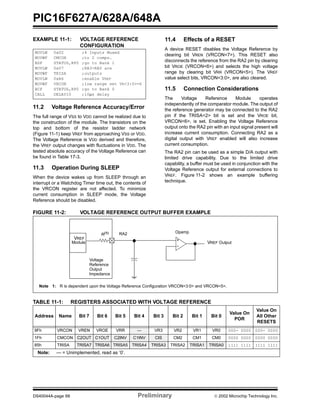
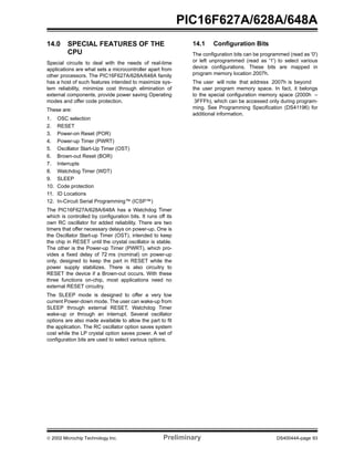
DS40044A-page 138 Preliminary 2002 Microchip Technology Inc.
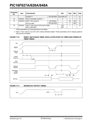
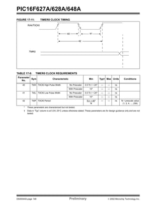
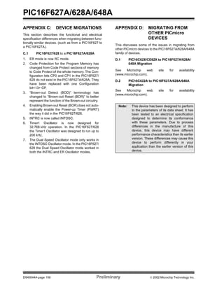
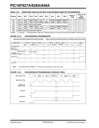
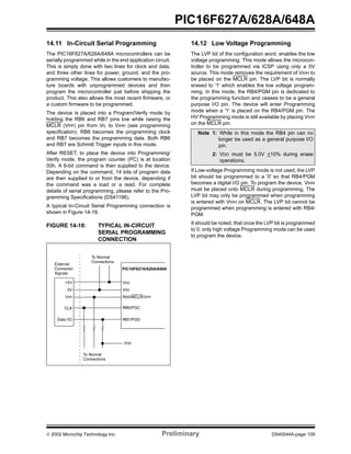
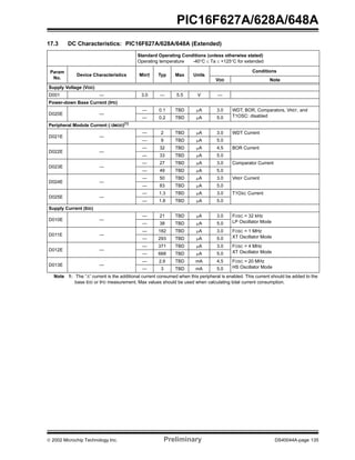
TABLE 17-2: COMPARATOR SPECIFICATIONS
TABLE 17-3: VOLTAGE REFERENCE SPECIFICATIONS
Operating Conditions: 2.0V < VDD <5.5V, -40°C < TA < +125°C, unless otherwise stated.
Param
No.
Characteristics Sym Min Typ Max Units Comments
D300 Input Offset Voltage VIOFF — ±5.0 ±10 mV
D301 Input Common Mode Voltage VICM 0 — VDD - 1.5* V
D302 Common Mode Rejection Ratio CMRR 55* — — db
D303 Response Time(1)
TRESP —
—
—
300
400
400
400*
600*
600*
ns
ns
ns
VDD = 3.0V to 5.5V
-40° to +85°C
VDD = 3.0V to 5.5V
-85° to +125°C
VDD = 2.0V to 3.0V
-40° to +85°C
D304 Comparator Mode Change to
Output Valid
TMC2OV — 300 10* µs
* These parameters are characterized but not tested.
Note 1: Response time measured with one comparator input at (VDD - 1.5)/2 while the other input transitions from
VSS to VDD.
Operating Conditions: 2.0V < VDD < 5.5V, -40°C < TA < +125°C, unless otherwise stated.
Spec
No.
Characteristics Sym Min Typ Max Units Comments
D310 Resolution VRES — — VDD/24
VDD/32
LSb
LSb
Low Range (VRR = 1)
High Range (VRR = 0)
D311 Absolute Accuracy VRAA —
—
—
—
1/4(2)
*
1/2(2)
*
LSb
LSb
Low Range (VRR = 1)
High Range (VRR = 0)
D312 Unit Resistor Value (R) VRUR — 2k* — Ω
D313 Settling Time(1)
TSET — — 10* µs
* These parameters are characterized but not tested.
Note 1: Settling time measured while VRR = 1 and VR<3:0> transitions from 0000 to 1111.
2: When VDD is between 2.0V and 3.0V the VREF output voltage levels on RA2 descirbed by the equa-
tion:[VDD/2 ± (3-VDD)/2] may cause the Absolute Accuracy (VRAA) of the VREF output signal on RA2 to be
greater than the stated max.](https://image.slidesharecdn.com/datasheet-151201210636-lva1-app6891/85/Datasheet-140-320.jpg)