Downloaded 11 times

![ENC28J60
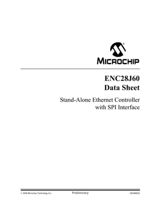
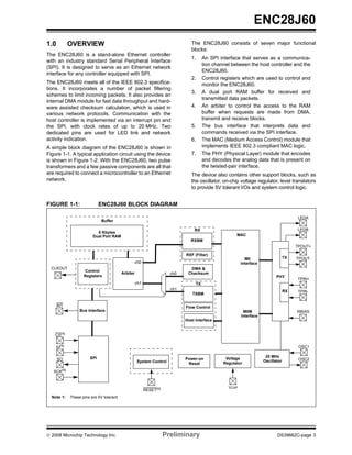
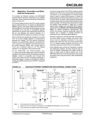
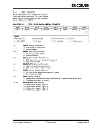
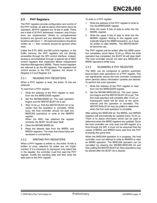
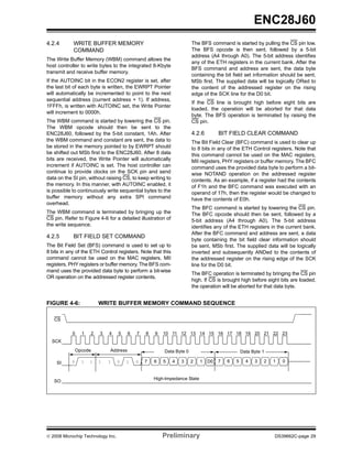
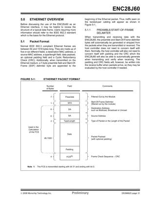
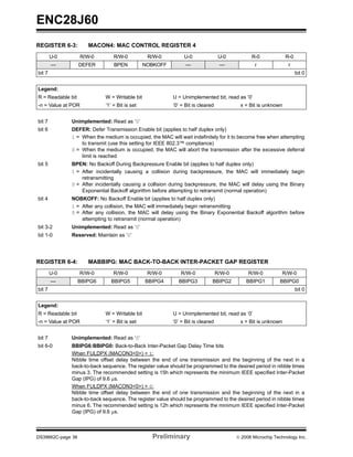
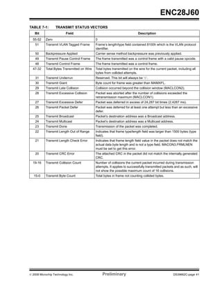
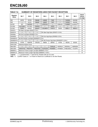
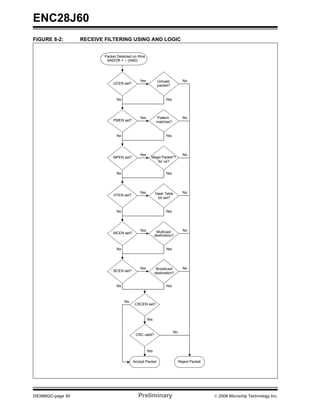
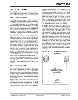
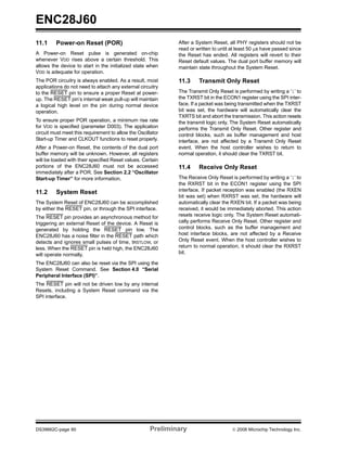
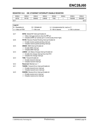
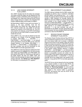
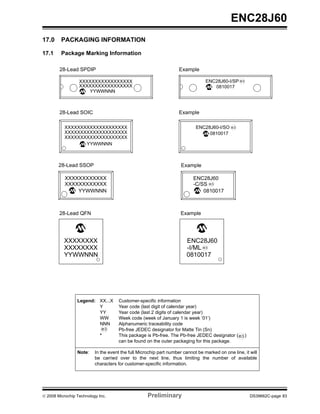
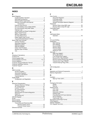
FIGURE 7-2: SAMPLE TRANSMIT PACKET LAYOUT
Buffer Pointers Address Memory Description
0120h 0Eh Control PHUGEEN, PPADN,
ETXST = 0120h
PCRCEN and POVERRIDE
0121h data[1]
0122h data[2]
Destination Address,
Data Packet Source Address,
Type/Length and Data
ETXND = 0156h 0156h data[m]
0157h tsv[7:0]
0158h tsv[15:8]
0159h tsv[23:16]
016Ah Status Vector
tsv[31:24] Status Vector
Written by the Hardware
016Bh tsv[39:32]
016Ch tsv[47:40]
016Dh tsv[55:48]
016Eh
Start of the Next Packet
To achieve the example layout shown in Figure 7-2 and DMA and transmission engine share the same memory
to transmit a packet, the host controller should: access port. Similarly, if the DMAST bit in ECON1 is set
1. Appropriately program the ETXST Pointer to after TXRTS is already set, the DMA will wait until the
point to an unused location in memory. It will TXRTS bit becomes clear before doing anything. While
point to the per packet control byte. In the the transmission is in progress, none of the unshaded
example, it would be programmed to 0120h. It is bits (except for the EECON1 register’s bits) in Table 7-2
recommended that an even address be used for should be changed. Additionally, none of the bytes to be
ETXST. transmitted should be read or written to through the SPI.
If the host controller wishes to cancel the transmission,
2. Use the WBM SPI command to write the per
it can clear the TXRTS bit.
packet control byte, the destination address, the
source MAC address, the type/length and the When the packet is finished transmitting or is aborted
data payload. due to an error/cancellation, the ECON1.TXRTS bit will
3. Appropriately program the ETXND Pointer. It be cleared, a seven-byte transmit status vector will be
should point to the last byte in the data payload. written to the location pointed to by ETXND + 1, the
In the example, it would be programmed to EIR.TXIF will be set and an interrupt will be generated
0156h. (if enabled). The ETXST and ETXND Pointers will not
be modified. To check if the packet was successfully
4. Clear EIR.TXIF, set EIE.TXIE and set EIE.INTIE
transmitted, the ESTAT.TXABRT bit should be read. If
to enable an interrupt when done (if desired).
it was set, the host controller may interrogate the
5. Start the transmission process by setting ESTAT.LATECOL bit in addition to the various fields in
ECON1.TXRTS. the transmit status vector to determine the cause. The
If a DMA operation was in progress while the TXRTS bit transmit status vector is organized as shown in
was set, the ENC28J60 will wait until the DMA opera- Table 7-1. Multi-byte fields are written in little-endian
tion is complete before attempting to transmit the format.
packet. This possible delay is required because the
DS39662C-page 40 Preliminary © 2008 Microchip Technology Inc.](https://image.slidesharecdn.com/datasheetenc28j60-110323021930-phpapp01/85/Datasheet-enc28j60-42-320.jpg)
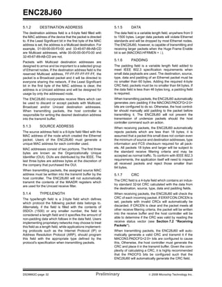
![ENC28J60
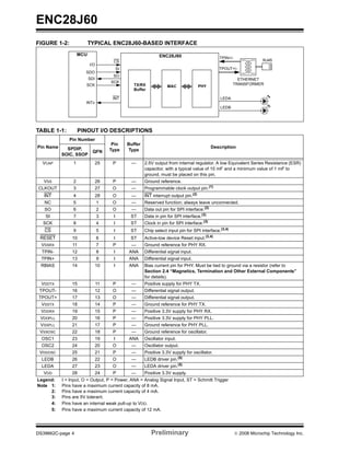
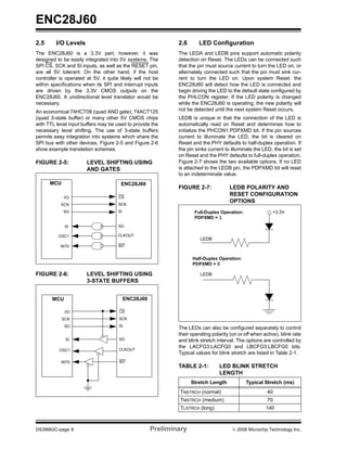
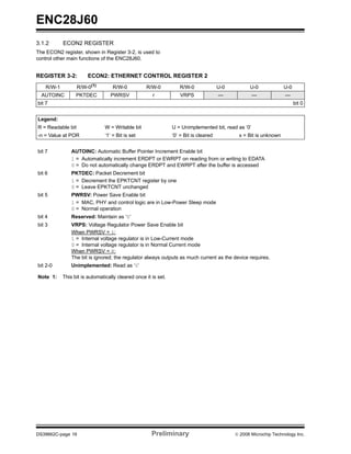
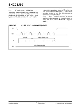
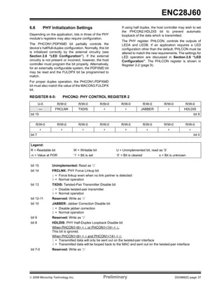
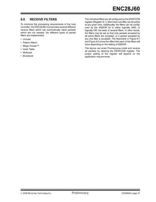
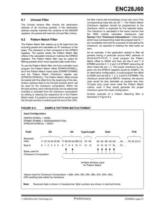
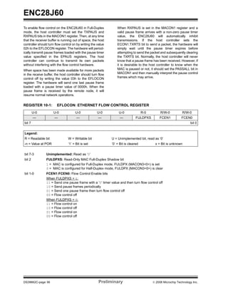
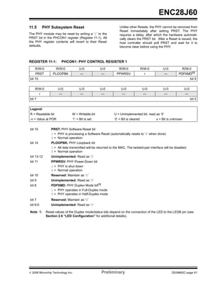
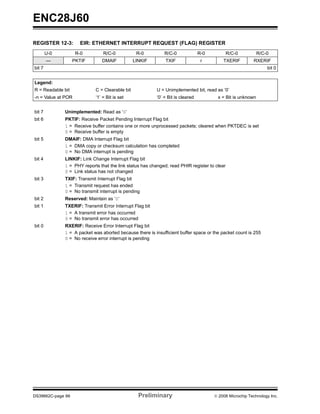
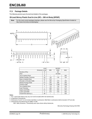
7.2 Receiving Packets After reception is enabled, packets which are not
filtered out will be written into the circular receive buffer.
7.2.1 ENABLING RECEPTION Any packet which does not meet the necessary filter
criteria will be discarded and the host controller will not
Assuming that the receive buffer has been initialized,
have any means of identifying that a packet was thrown
the MAC has been properly configured and the receive
away. When a packet is accepted and completely
filters have been configured to receive Ethernet
written into the buffer, the EPKTCNT register will incre-
packets, the host controller should:
ment, the EIR.PKTIF bit will be set, an interrupt will be
1. If an interrupt is desired whenever a packet is generated (if enabled) and the Hardware Write Pointer,
received, set EIE.PKTIE and EIE.INTIE. ERXWRPT, will automatically advance.
2. If an interrupt is desired whenever a packet is
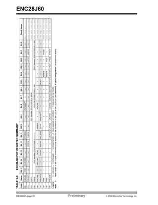
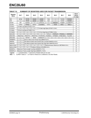
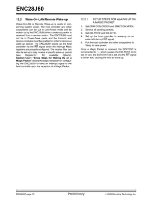
dropped due to insufficient buffer space, clear 7.2.2 RECEIVE PACKET LAYOUT
EIR.RXERIF and set both EIE.RXERIE and Figure 7-3 shows the layout of a received packet. The
EIE.INTIE packets are preceded by a six-byte header which
3. Enable reception by setting ECON1.RXEN. contains a Next Packet Pointer, in addition to a receive
After setting RXEN, the Duplex mode and the Receive status vector which contains receive statistics, includ-
Buffer Start and End Pointers should not be modified. ing the packet’s size. This receive status vector is
Additionally, to prevent unexpected packets from arriv- shown in Table 7-3.
ing, it is recommended that RXEN be cleared before If the last byte in the packet ends on an odd value
altering the receive filter configuration (ERXFCON) and address, the hardware will automatically add a padding
MAC address. byte when advancing the Hardware Write Pointer. As
such, all packets will start on an even boundary.
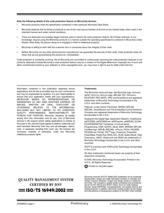
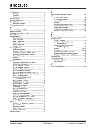
FIGURE 7-3: SAMPLE RECEIVE PACKET LAYOUT
Address Memory Description
Packet N – 1 End of the Previous Packet
101Fh
1020h 6Eh Low Byte
Next Packet Pointer
1021h 10h High Byte
1022h rsv[7:0] status[7:0]
1023h rsv[15:8] status[15:8]
Receive Status Vector
1024h rsv[23:16] status[23:16]
1025h rsv[30:24] status[31:24]
1026h data[1]
1027h data[2]
Packet N
Packet Data: Destination Address,
Source Address, Type/Length, Data,
Padding, CRC
1059h data[m-3] crc[31:24]
106Ah data[m-2] crc[23:16]
106Bh data[m-1] crc[15:8]
106Ch data[m] crc[7:0]
106Dh Byte Skipped to Ensure
Even Buffer Address
106Eh
Packet N + 1 Start of the Next Packet
© 2008 Microchip Technology Inc. Preliminary DS39662C-page 43](https://image.slidesharecdn.com/datasheetenc28j60-110323021930-phpapp01/85/Datasheet-enc28j60-45-320.jpg)


The ENC28J60 is a stand-alone Ethernet controller with an SPI interface. It contains an 8KB transmit/receive packet buffer, MAC and PHY modules to implement 10Base-T Ethernet connectivity. It interfaces to a host processor via SPI and interrupts. Key features include packet filtering, internal DMA, and hardware assisted checksum calculation to support Ethernet networking.


