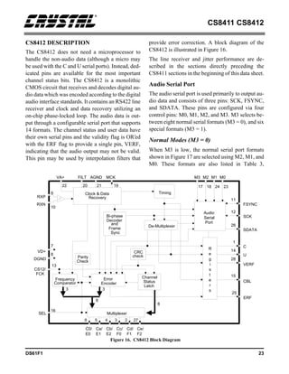
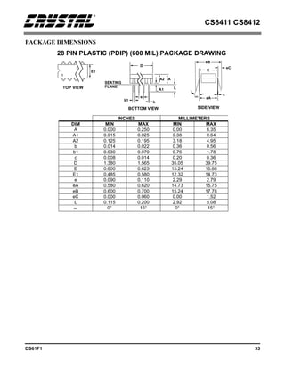
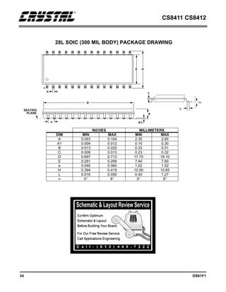
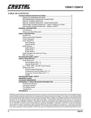
The document describes the CS8411/12, monolithic CMOS digital audio interface receivers that support various audio data formats including AES/EBU and IEC958. These devices feature low-jitter clock recovery, extensive error reporting, and a configurable buffer memory for the CS8411, while the CS8412 directly outputs demultiplexed data. Additionally, it includes detailed technical specifications, operating conditions, and compliance with established audio interface standards.
![CS8411 CS8412
12 DS61F1
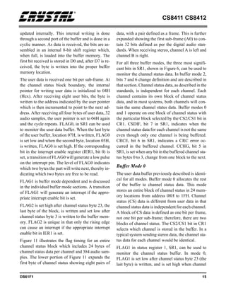
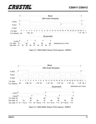
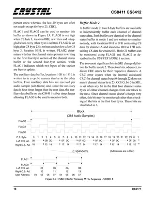
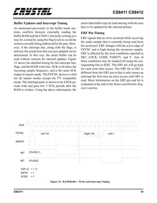
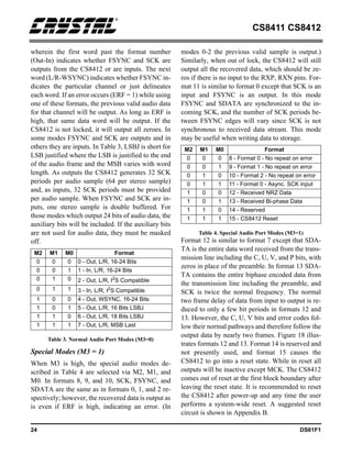
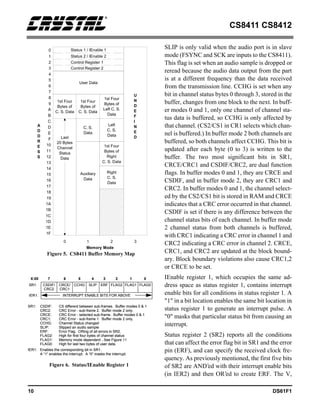
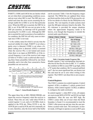
high. B0 and B1 select one of three buffer modes
listed in Table 2 and illustrated in Figure 5. In all
modes four bytes of user data are stored. In mode 0,
one entire block of channel status is stored. In mode
1 eight bytes of channel status and sixteen bytes of
auxiliary data are stored. In mode 2, eight bytes of
channel status from each sub-frame are stored. The
buffer modes are discussed in more detail in the
Buffer Memory section. The next bit, CS2/CS1, se-
lects the particular sub-frame of channel status to
buffer in modes 0 and 1, and has no effect in mode
2. When CS2/CS1 is low, sub-frame 1 is buffered,
and when CS2/CS1 is high, sub-frame 2 is buff-
ered. IER/SR selects which set of registers, either
IEnable or status, occupy addresses 0 and 1. When
IER/SR is low, the status registers occupy the first
two addresses, and when IER/SR is high, the IEn-
able registers occupy those addresses. FCEN en-
ables the internal frequency counter. A 6.144 MHz
clock must be connected to the FCK pin as a refer-
ence. The value of the FREQ bits in SR2 are not
valid until two thirds of a block of data is received.
Since FCK and A4, the most significant address bit,
occupy the same pin, A4 is internally set to zero
when FCEN is high. Since A4 is forced to zero, the
upper half of the buffer is not accessible while us-
ing the frequency compare feature. FPLL deter-
mines how FSYNC is derived. When FPLL is low,
FSYNC is derived from the incoming data, and
when FPLL is high, it is derived from the internal
phase-locked loop.
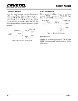
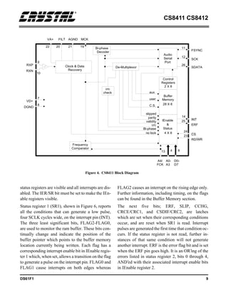
Control Register 2 configures the serial port which
consists of three pins: SCK, SDATA, and FSYNC.
SDATA is always an output, but SCK and FSYNC
can be configured as inputs or outputs. FSYNC and
SDATA can have a variety of relationships to each
other, and the polarity of SCK can be controlled.
The large variety of audio data formats provides an
easy interface to most DSPs and other audio pro-
cessors. SDATA is normally just audio data, but
special modes are provided that output received bi-
phase data, or received NRZ data with zeros substi-
tuted for preamble. Another special mode allows an
asynchronous SCK input to read audio data from
the serial port without slipping samples. In this
mode FSYNC and SDATA are outputs synchro-
nized to the SCK input. Since SCK is asynchronous
to the received clock, the number of SCK cycles
between FSYNC edges will vary.
ROER, when set, causes the last audio sample to be
reread if the error pin, ERF, is active. When out of
lock, the CS8411 will output zeros if ROER is set
and output random data if ROER is not set. The
conditions that activate ERF are those reported in
SR2 and enabled in IER2. Figure 10 illustrates the
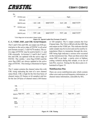
modes selectable by SDF2-SDF0 and FSF1-FSF0.
MSTR, which in most applications will be set to
one, determines whether FSYNC and SCK are out-
puts (MSTR = 1) or inputs (MSTR = 0). When
FSYNC and SCK are inputs (slave mode) the audio
Figure 8. Control Register 1
CR1: FPLL: 0 - FSYNC from RXP/RXN, 1 - FSYNC from PLL
FCEN: enables freq. comparator (FCK must be 6.144 MHz).
IER/SR: [X:00,01] 0 - status, 1 - interrupt enable registers.
CS2/CS1: ch. status to buffer; 0 - sub-frame 1, 1 - sub-frame 2.
B1: with B0, selects the buffer memory mode.
B0: with B1, selects the buffer memory mode.
RST: Resets internal counters. Set to “1” for normal operation.
X:02 7 6 5 4 3 2 1 0
CR1. FPLL FCEN IER/SR CS2/CS1 B1 B0 RST
B1 B0 Mode Buffer Memory Contents
0 0 0 Channel Status
0 1 1 Auxiliary Data
1 0 2 Independent Channel Status
1 1 3 Reserved
Table 2. Buffer Memory Modes
Figure 9. Control Register 2
CR2: ROER: Repeat previous value on error (audio data)
SDF2: with SDF0 & SDF1, select serial data format.
SDF1: with SDF0 & SDF2, select serial data format.
SDF0: with SDF1 & SDF2, select serial data format.
FSF1: with FSF0, select FSYNC format.
FSF0: with FSF1, select FSYNC format.
MSTR: When set, SCK and FSYNC are output
SCED: When set, falling edge of SCK outputs data.
When clear, rising edge of SCK outputs data.
X:03 7 6 5 4 3 2 1 0
CR2. ROER SDF2 SDF1 SDF0 FSF1 FSF0 MSTR SCED](https://image.slidesharecdn.com/cs8411-240822040358-5a362a3f/85/CS8411-Data-sheet-for-enginering-and-electric-technology-12-320.jpg)