Downloaded 90 times


![© Dr. Lynn Fuller, Motorola Professor
Rochester Institute of Technology
Microelectronic Engineering
GaAs Device Technology
Page 18
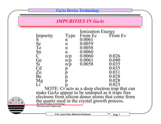
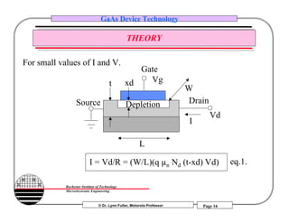
THEORY
Gate
Source Drain
L
Id
W
t xd
Vd
For larger values of I and V.
Depletion
Id = Go { V -2/3(2εs/qNdt2)0.5 [(Ψo-Vg+Vd)1.5 - (Ψo-Vg )1.5]}
Vg
eq. 2.](https://image.slidesharecdn.com/gaas-150924090435-lva1-app6891/85/Gaas-18-320.jpg)
![© Dr. Lynn Fuller, Motorola Professor
Rochester Institute of Technology
Microelectronic Engineering
GaAs Device Technology
Page 19
THEORY
Gate
Source Drain
L
Isat
W
t
Vd
For Pinch Off
Channel Pinched Off
Isat = Go [ qNd t2 - (Ψo-Vg ){1- 2/3[2εs (Ψo-Vg ) ]0.5}]
Depletion
Vg
qNdt26εs
eq. 3.](https://image.slidesharecdn.com/gaas-150924090435-lva1-app6891/85/Gaas-19-320.jpg)


This document is a presentation by Dr. Lynn Fuller on Gallium Arsenide (GaAs) devices, technologies, and integrated circuits. It provides an overview and comparison of silicon and GaAs, describes GaAs crystal growth techniques like molecular beam epitaxy (MBE), and discusses GaAs field effect transistors (MESFETs) and the fabrication process for GaAs integrated circuits. The presentation contains numerous diagrams and equations to illustrate concepts in GaAs device physics and fabrication processes.


