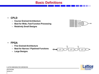
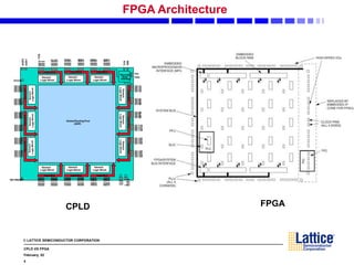
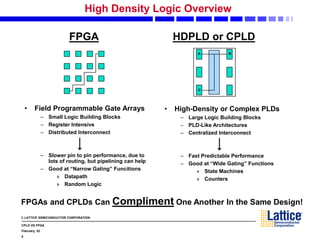
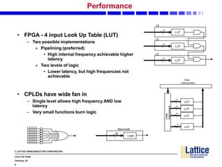
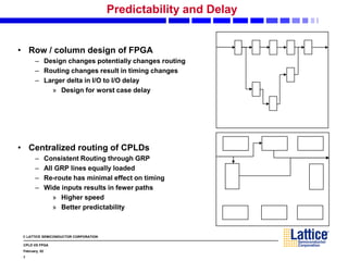
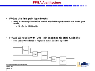
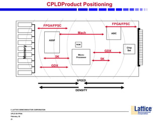
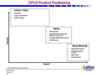
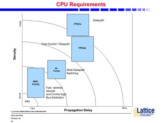
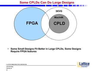
More Related Content
Similar to cpld vs fpga Positionning presentation.ppt
Similar to cpld vs fpga Positionning presentation.ppt (20)
cpld vs fpga Positionning presentation.ppt
- 2. © LATTICE SEMICONDUCTOR CORPORATION
CPLD VS FPGA
February, 02
2
Agenda
• Architecture Descriptions
– CPLD
– FPGA
– Advantages / Disadvantages
• Gate Counting
• Common Terms
• Positioning
- 3. © LATTICE SEMICONDUCTOR CORPORATION
CPLD VS FPGA
February, 02
3
Basic Definitions
• CPLD
– Course Grained Architecture
– Best for Wide, Fast Function Processing
– Relatively Small Designs
• FPGA
– Fine Grained Architecture
– Best for Narrow / Pipelined Functions
– Large Designs
LUT
4
LUT LUT
- 4. © LATTICE SEMICONDUCTOR CORPORATION
CPLD VS FPGA
February, 02
4
FPGA Architecture
FPGA
CPLD
Global Routing Pool
(GRP)
Boundary
Scan
Interface
SET/RESET
TDI
TDO
VCCIO
Input Bus
Generic
Logic Block
Input Bus
Generic
Logic Block
Input Bus
Input Bus
Input Bus Input Bus
Generic
Logic Block
Generic
Logic Block
Generic
Logic Block
Generic
Logic Block
Input
Bus
Generic
Logic
Block
Input
Bus
Generic
Logic
Block
Input
Bus
Generic
Logic
Block
I/O 72
I/O 73
I/O 74
I/O 75
I/O 92
I/O 93
I/O 94
I/O 95
I/O 96
I/O 97
I/O 98
I/O 99
I/O 116
I/O 117
I/O 118
I/O 119
I/O 120
I/O 121
I/O 122
I/O 123
I/O 140
I/O 141
I/O 142
I/O 143
I/O 239
I/O 238
I/O 237
I/O 236
I/O 219
I/O 218
I/O 217
I/O 216
I/O 263
I/O 262
I/O 261
I/O 260
I/O 243
I/O 242
I/O 241
I/O 240
I/O 287
I/O 286
I/O 285
I/O 284
I/O 267
I/O 266
I/O 265
I/O 264
- 5. © LATTICE SEMICONDUCTOR CORPORATION
CPLD VS FPGA
February, 02
5
High Density Logic Overview
• Field Programmable Gate Arrays
– Small Logic Building Blocks
– Register Intensive
– Distributed Interconnect
– Slower pin to pin performance, due to
lots of routing, but pipelining can help
– Good at “Narrow Gating” Funcitions
» Datapath
» Random Logic
• High-Density or Complex PLDs
– Large Logic Building Blocks
– PLD-Like Architectures
– Centralized Interconnect
– Fast Predictable Performance
– Good at “Wide Gating” Functions
» State Machines
» Counters
A B
C
FPGA HDPLD or CPLD
FPGAs and CPLDs Can Compliment One Another In the Same Design!
- 6. © LATTICE SEMICONDUCTOR CORPORATION
CPLD VS FPGA
February, 02
6
Performance
• FPGA - 4 input Look Up Table (LUT)
– Two possible implementations
» Pipelining (preferred)
• High internal frequency achievable higher
latency
» Two levels of logic
• Lower latency, but high frequencies not
achievable
• CPLDs have wide fan in
– Single level allows high frequency AND low
latency
– Very small functions burn logic
LUT
LUT
LUT
4
4
4
LUT
4
Local
Interconnect
Row
Interconnect
Local
Interconnect
LUT
4
LUT
4
LUT
4
LE
LE
LE
Logic
68
Macrocell
- 7. © LATTICE SEMICONDUCTOR CORPORATION
CPLD VS FPGA
February, 02
7
Predictability and Delay
• Row / column design of FPGA
– Design changes potentially changes routing
– Routing changes result in timing changes
– Larger delta in I/O to I/O delay
» Design for worst case delay
• Centralized routing of CPLDs
– Consistent Routing through GRP
– All GRP lines equally loaded
– Re-route has minimal effect on timing
– Wide inputs results in fewer paths
» Higher speed
» Better predictability
- 8. © LATTICE SEMICONDUCTOR CORPORATION
CPLD VS FPGA
February, 02
8
FPGA Architecture
• FPGAs use fine grain logic blocks
– Many of these logic blocks are used to implement logic functions due to fine grain
blocks,
» 16 LBs for 16-Bit adder
• FPGAs Work Best With One - hot encoding for state functions
– Fine Grain / Abundance of Registers makes One-Hot a good fit
Register
Register
Register
Logic
Logic
- 9. © LATTICE SEMICONDUCTOR CORPORATION
CPLD VS FPGA
February, 02
9
FPGA EPROM
• Most FPGAs are volatile SRAM
• Devices are reprogrammed on power-up
– Program can be stored in companion, EPROM next to FPGAs
– Device can be programmed with P via Flash programming
– Logic is not available when power is initially applied
FPGA
EPROM
or P
- 10. © LATTICE SEMICONDUCTOR CORPORATION
CPLD VS FPGA
February, 02
10
FPGA Vs CPLD Logic Element
• FPGA Has a Basic, Fine Grain Logic Element
– Typical FPGA has 4 Inputs and 8 Product Terms Per Logic Element
– Wide Designs Speed Limitation Can be Overcome with Pipelining
• CPLD Has Complex Logic Element
– 5KVG Family has 68 Inputs and 32 Product Terms Per Logic Element
– The CPLD Has Less Registers but uses these registers more efficiently
– Simple Designs Use up the Registers and Logic Elements are Under
Utilized
Logic
Element
8 PTs
FPGA
4 1
Logic
Element
32 PTs
CPLD
68 1
CPLD vs FPGA Input Ratio = 17 : 1
CPLD vs FPGA Product Term Ratio = 4 : 1
- 11. © LATTICE SEMICONDUCTOR CORPORATION
CPLD VS FPGA
February, 02
11
Technology Comparisons
Feature E2
CMOS Flash SRAM Antifuse
Reprogrammability Yes Yes Yes NO
In-System Programmable Yes Yes Yes NO
(Volatile)
Program Time Fast Med. Fast Slow
Erase Time Fast Slow Fast N/A (OTP)
Testability Full Full Full Limited
External Hardware No No EPROM Pgmr
- 13. © LATTICE SEMICONDUCTOR CORPORATION
CPLD VS FPGA
February, 02
13
CPLD Vs. FPGA Fitting
• Number of PLD Gates or Registers Doesn’t Tell the Entire Story,
The Application Does
– Even among equivalent product types, Gate count is “specsmanship”, the only
real way to see if a design will fit or fit better is to run it!
• Applications Needing High Speed and Predictability Should Use
CPLD
• Large Register Intensive Logic Applications Should Use FPGA
• Most Designs Have a Mixture of Qualities that Could Fit Either, So
Both CPLD and FPGA Should Be Considered
- 14. © LATTICE SEMICONDUCTOR CORPORATION
CPLD VS FPGA
February, 02
14
A Gate Is a Gate Is a Gate
• FPGA and CPLD Both Build Gates Out of Transistors
• The Basic CMOS Gates Are the Same in Both Architectures
– Inverter
– NAND
– NOR
• Example NAND
B
A
F
VCC
B
A
F
- 15. © LATTICE SEMICONDUCTOR CORPORATION
CPLD VS FPGA
February, 02
15
CPLD Gate Count Vs FPGA Gate Count
• It is Difficult to Compare Apples to Apples
• What Is an “Equivalent PLD Gate”?
– A Simple PLD Gate Is Considered 2-input AND
• How Many Simple PLD Gates to Build an 8-input
AND?
– Seven
• FPGA Vendors Have Different Standards for Gate
Counts
– A Higher Percentage of Gates Are Used for Interconnect in FPGA
and some Vendors count Memory in Total Gate Count
• The First Order of Importance Is to Have Enough
Registers to Compete, Not Fight Over Gate Counts
• The Only Way To Know if a Design
Fits is to FIT IT!!!
- 17. © LATTICE SEMICONDUCTOR CORPORATION
CPLD VS FPGA
February, 02
17
FPGA Terms
• FPGA - Field Programmable Gate Array
• SRAM - Static RAM
– Program stored in outside EPROM, intelligent controller or through JTAG Port,
FPGAs must be reprogrammed on every power-up
• Configuration EPROM
– External hardware used to hold FPGA programming file
• ICR - In-Circuit Reconfigurability
• Anti-fuse - One-Time Programmable (OTP)
– (Quicklogic and Actel)
• Interconnect - Basic Routing element
– FPGAs rely on a Fine Grain routing structure
• LUT - Look-Up Table
– 4-input SRAM based look-up table produces the output of any 4 input function
• LE/CLB - Logic Element
– Smallest logic unit. 4 input Look-Up Table, Carry/cascade chains, register and
register control signals
- 18. © LATTICE SEMICONDUCTOR CORPORATION
CPLD VS FPGA
February, 02
18
FPGA Terms
• LAB - Logic Array Block (Altera)
– Consists of 8 LEs and associated control signals and routing
• EAB - Embedded Array Block (Altera)
– High level building block, includes Ram and registers
• One Hot Encoding
– When single registers (bits) are used to represent states instead of the common
binary method
– Example: 20 state-state machine
» One Hot: 20 registers (bits)
» Binary: 5 registers (bits)
• Pipeline
– Putting functions in an “assembly line” format. Small portions done quickly allows
a high clock speed and results at short intervals. The drawback is results take
longer to get from input to output (latency)
Register Register Register Register
1 Clk Delay 3 Clk Delay
2 Clk Delay
No Clk Delay
- 19. © LATTICE SEMICONDUCTOR CORPORATION
CPLD VS FPGA
February, 02
19
FPGA Terms
• SoC
– System on a Chip
• MPI
– Microprocessor Interface
• EBR
– Embedded Block RAM
• PLC
– Programmable Logic Cell
• PIO
– Programmable Input/Output Cells
• CIB
– Common Interface Block
• PFU
– Programmable Function Unit
• SLIC
– Decoder / PAL like logic
- 21. © LATTICE SEMICONDUCTOR CORPORATION
CPLD VS FPGA
February, 02
21
CPLDProduct Positioning
Memory
Micro-
Processor
ASSP
ROM
ASIC
Chip
Set
SPEED
Mach
5K
5K
FPGA/FPSC
GDX
DENSITY
FPGA/FPSC
GDX
- 22. © LATTICE SEMICONDUCTOR CORPORATION
CPLD VS FPGA
February, 02
22
CPLD Product Positioning
Mach/Mach4K
• High Speed Decode
• Small High speed
Control
• ASIC Fixes
• PCI Arbitration
FPGA / FPSC
• Data Path
• Logic consolidation
• DSP Functions
5KVG
• Wide Decode
• Buss Control (16-32-64 bit
Buses) In One Level
• Complex High Speed Control
• Fast Muxing
Speed
Density
- 23. © LATTICE SEMICONDUCTOR CORPORATION
CPLD VS FPGA
February, 02
23
CPU Requirements
Propagation Delay
Density
CPU
5K
Family
Fast Slow
M4K
Family
FPGAs
Fast address
decode
and Control logic
Bus Arbitration
Wide Datapath
Switching
Fast Control / Datapath
Datapath
Small
Large
FPSCs
- 24. © LATTICE SEMICONDUCTOR CORPORATION
CPLD VS FPGA
February, 02
24
Some CPLDs Can Do Large Designs
• Some Small Designs Fit Better in Large CPLDs, Some Designs
Require FPGA features
FPGA
Mach4K
5KVG
CPLD
- 25. © LATTICE SEMICONDUCTOR CORPORATION
CPLD VS FPGA
February, 02
25
Summary
• Understand the Design
– Don’t Assume the Best Hardware is an FPGA or CPLD
• CPLDs Are Best Suited for:
– Wide Designs
– Speed Critical, Low Latency, Low Skew
– Relatively Small
– Hot-Plugable
• FPGAs Are Best Suited for:
– Large Register Intensive Designs
– Narrow Gating, Pipeline-able
• Fit the Design to Determine the Size in Our Devices