

Recommended
More Related Content
What's hot
What's hot (20)
Similar to Giao trinh he thong nhung vdk h8
Similar to Giao trinh he thong nhung vdk h8 (20)
Recently uploaded
Recently uploaded (20)
Giao trinh he thong nhung vdk h8
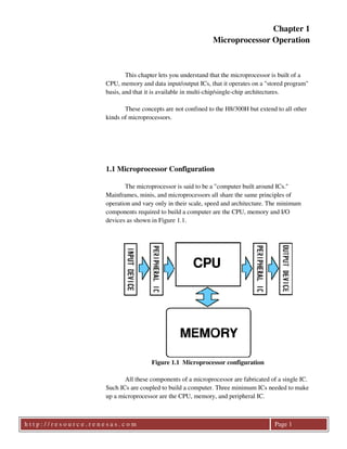
- 1. Chapter 1 Microprocessor Operation This chapter lets you understand that the microprocessor is built of a CPU, memory and data input/output ICs, that it operates on a "stored program" basis, and that it is available in multi-chip/single-chip architectures. These concepts are not confined to the H8/300H but extend to all other kinds of microprocessors. 1.1 Microprocessor Configuration The microprocessor is said to be a "computer built around ICs." Mainframes, minis, and microprocessors all share the same principles of operation and vary only in their scale, speed and architecture. The minimum components required to build a computer are the CPU, memory and I/O devices as shown in Figure 1.1. Figure 1.1 Microprocessor configuration All these components of a microprocessor are fabricated of a single IC. Such ICs are coupled to build a computer. Three minimum ICs needed to make up a microprocessor are the CPU, memory, and peripheral IC. h t t p : / / r e s o u r c e . r e n e s a s . c o m Page 1
- 2. CPU (Central Processing Unit) The CPU forms the nucleus of any computer by executing instructions. Microprocessors are grouped into 4-bit, 8-bit, 16-bit, and 32-bit microprocessors according to the length of bits they can handle at a time. A 4- bit microprocessor can handle four binary digits in a single instance of calculation, but as many as eight digits in two instances and 16 in four instances. The microprocessor is also known as a "MPU (microprocessing unit)", "microprocessor", or simply "processor." Memory (Memory) A device on which instructions and data are stored. Without memory, programs and data cannot be used. In a microprocessor, ROM (read-only memory) and RAM (random access memory) are used. Input device (Input) A data input device. The keyboard and mouse of a PC, for example, are data input devices. With a built-in controller, switches and sensors are input devices. These input devices cannot be directly connected to a CPU, but they must be attached to the CPU by way of a "peripheral IC," containing connection circuitry. Depending on the kind of input device to be connected to the CPU, an appropriate peripheral IC is used. Output device (Output) A data output device. The display and printer of a PC, for example, are data output devices. With a built-in controller, display LEDs, motors, heaters and so on are output devices. Like input devices, output devices are attached to a CPU by way of a "peripheral IC." Depending on the kind of output device to be connected to the CPU, an appropriate peripheral IC is used. Input devices and output devices are collectively called "peripherals." 1.2 Stored Program Computers The stored program computer provides a most precise concept of the operating principles of a computer. It might be safely said that "All modern computers are stored program computers." The stored program computer was first conceptualized in 1947 by John von Neumann and is also known as a "Neumann computer." In the stored program computer, the CPU reads instructions stored in memory in sequence, decodes and executes them. The act of the CPU reading an instruction from memory is called "fetch." Interpreting the fetched instruction to see what operation it defines is called "decode." The CPU then proceeds to perform, or "execute," the operation defined by the instruction. When the CPU has finished executing the h t t p : / / r e s o u r c e . r e n e s a s . c o m Page 2
- 3. instruction, it fetches the next instruction. After all, the CPU infinitely repeats the following cycle of operations: - Instruction fetch - Instruction decoding - Instruction execution Any microprocessor has a program counter in its CPU. The program counter always holds the "address of the next instruction to be executed." When the CPU reads an instruction, the program is automatically updated to indicate the address of the next instruction in sequence. The program counter thus ensures that instructions stored in memory will be executed in correct sequence. Figure 1.2 Operating principles of a stored program computer 1.3 Memory Memory devices are broadly classified into two categories: ROM (read-only memory) and RAM (random access memory). You can only read stored data from ROM but cannot write to it. Stored data is preserved intact, however, when the microprocessor is switched off. Use ROM to store valuable data that needs to be protected from erasure in times of power failures, typically, programs. Instructions are stored in ROM. Each meaningful collection of instructions is a program. Any microprocessor would be inoperable unless it comes up with "programs available for ready use" when switched on. ROM fills this need. Data can be written to and read from RAM as desired. Stored data would be lost, however, once the microprocessor is switched off. Even when h t t p : / / r e s o u r c e . r e n e s a s . c o m Page 3
- 4. the microprocessor is switched on again, previous data is no longer left. Hence, RAM is used as temporary data storage. Programs may also be placed in RAM, but will be lost once the microprocessor is switched off. To run programs in RAM, it is necessary to attach an external storage device, such as a floppy disk or hard disk drive, and transfer the programs to RAM from external storage to RAM when the microprocessor is switched on. Mask ROM (Mask ROM) When a memory IC is manufactured in the factory, programs are written to it. A mask is a plate of glass imprinted with patterns of wirings and transistors used in the IC manufacturing process. Users have a semiconductor manufacture custom-build a mask to manufacture a memory IC. Advantages - Suitable for volume production - Low cost Disadvantages - Long lead-time from ordering to completion - Not reprogrammable once built EPROM (Erasable & Programmable ROM) Stored data can be erased by ultraviolet irradiation. To this end, a special package with a glass window is used. An EPROM writer is used to write to EPROM. EPROM is erasable and programmable about 100 times. Advantage - Erasable and programmable and thus convenient for testing and debugging Disadvantage - Expensive because of the use of a special package OTPROM (One Time Programmable ROM) An EPROM chip housed in an inexpensive plastic package. Stored data cannot be erased by ultraviolet irradiation because no glass window can be attached to the plastic package. OPTROM can be written only once, but it comes by far cheaper than EPROM. Programs are debugged in EPPROM and, when finalized, moved to OTPROM for volume production. Advantage - Cheaper than EPROM and suitable for small-batch production Disadvantage - Not erasable and programmable EEPROM (Electrically Erasable & Programmable ROM) EEPROM can be electrically erased and programmable, and can be reprogrammed when mounted on a board as a finished product. EEPROM is reprogrammable about tens of thousand times. h t t p : / / r e s o u r c e . r e n e s a s . c o m Page 4
- 5. Advantages - Onboard reprogrammable - Ready for infinite times of reprogramming Disadvantage - Expensive Flash memory (Flash Memory) A variation of flash memory, which is cheaper and larger-sized. Advantage - Cheaper and larger-sized than EEPROM Disadvantages - Unable to write address by address, unlike EEPROM - Memory IC divided into blocks for erasure and reprogramming block by block Static RAM (Static RAM) RAM with its storage circuit built of flip-flops. Given a supply voltage, static RAM preserves stored data intact. It dissipates least power when out of use. Because six transistors are used to build its flip-flops, static RAM offers less storage capacity than does ROM. Advantages - Fast - Low power consumption and suitable for battery backup Disadvantages - Expensive - Small storage capacity Dynamic RAM (Dynamic RAM) Simplified storage circuitry with only one capacitor and one transistor to provide each bit of memory, and hence larger-sized than static RAM. Charges on the capacitors, however, drain with time, resulting ultimately in loss of stored data. Before such loss, all stored data must be read out and refreshed. Power alone does not allow dynamic RAM to retain stored data but requires refreshing for that purpose. Advantage - Cheap and large-sized Disadvantage - Refreshing required Table 1.1 summarizes features of key ROM and RAM devices. h t t p : / / r e s o u r c e . r e n e s a s . c o m Page 5
- 6. Table 1.1 Kinds and features of memory devices Kind Features ROM Mask ROM Large-sized, cheap, volume production use, custom fabrication, not reprogrammable EPROM Programmable and erasable by ultraviolet irradiation. Testing, debugging OTPROM Low-volume production use, one-time programmable EEPROM Electrically programmable, onboard reprogrammable Flash memory Electrically erasable and programmable, cheaper and larger sized than EEPROM RAM Static RAM Stored data preserved under voltage input alone, fast, battery backup use Dynamic RAM Refreshing required to preserve data, large-sized, cheap 1.4 Single-Chip/Multi-Chip Microprocessors Putting a CPU, ROM, RAM, and data input/output circuitry into a single IC will make a single-chip microprocessor. Single-chip microprocessors come compact and cheap, but do not allow users to choose built-in functions at their option. Single-chip microprocessors are also known as "microcomputer units (MCUs)," because they are made of a single IC. On the other hand, a computer fabricated from a mix of a CPU, memory and data input/output devices is called a "multi-chip microprocessor." Multi-chip microprocessors offer users greater freedom in their component choice. Multi-chip microprocessors will prove more advantageous for larger systems involving complexities of input/output. See how a single-chip microprocessor and a multi-chip microprocessor differ in Figure 1.3. h t t p : / / r e s o u r c e . r e n e s a s . c o m Page 6
- 7. Figure 1.3 Single-chip microprocessor and multi-chip microprocessor Single-chip microprocessors are used as built-in controllers. When a single-chip microprocessor is switched on, the control program stored in its internal ROM launches instantly. Internal RAM is used as temporary storage. The internal data input/output circuits, too, have been chosen to support the single-chip microprocessor as s controller. Kinds of internal ROM Early single-chip microprocessors included only mask ROM and were available only for use in mass-produced products. Subsequently EPROM has made inroads into single-chip microprocessors as internal ROM. As testing and debugging was carried out in erasable and programmable packages with windows and inexpensive plastic-packaged OTPROM used on commercialization, single-chip microprocessors came to be used in products manufactured in small batches as well. Now, single-chip microprocessors with internal EEPROM and flash memory are available for use in various applications. As the IC manufacturing technology has been advancing from year to year, with continuing increases in the sizes of internal ROM and RAM, state-of-the-art data input/output functions have been used in single-chip microprocessors in an expanding of applications. Microprocessors and memory A memory device organized into 8 bits per address is used. Each sequence of 8 bits is called a "byte," and memory sizes are stated in the unit byte. 64K bytes of memory could be connected to classical 8-bit microprocessors as standard. This memory size indicates 8 bits per address in a memory space of 64K (65536 addresses). Eight bits of memory per address are h t t p : / / r e s o u r c e . r e n e s a s . c o m Page 7
- 8. also connected to 16- and 32-bit microprocessors, as well as 8-bit microprocessors. 1. What are the three key ICs needed to make up a microprocessor? (CPU (MPU ) ) (Memory ) (Peripheral IC) Mainframes and minis share the same computer architecture. Microprocessors are characterized by the fact that three components of the computer - namely, the CPU, memory, and input/output circuit (peripheral IC) - are each fabricated as an IC. 2. Fill the blanks with appropriate words or phrases. The (stored program computer) provides a most precise concept of the operating principles of a computer. This was first conceptualized in 1947 by (John von Neumann). The stored program computer materializes the principles of a computer in which the CPU reads instructions from memory and executes them. This is also known as a "Neumann computer," because of its conceptualization by John von Neumann. 3. Mention one advantage and one disadvantage for each of the following kinds of memory: Mask ROM Advantage (Inexpensive, large-sized ) Disadvantage (Available only on order, not reprogrammable) EPROM Advantage (Erasable and programmable) Disadvantage (Expensive ) Dynamic RAM Advantage (Inexpensive, large-sized ) Disadvantage (Refreshing required ) Mask ROM is volume-produced at factory at low cost, and features circuit simplicity, offering large-sized memory. Mask ROM can be manufactured only by order and is not reprogrammable after it is built. EPROM allows about 100 times of erasure and reprogramming using a special writer, but the special package with a glass window adds to its cost. Using capacitors as storage devices, DRAM is simple in circuitry, inexpensive, and large-sized, but what is inconvenient, it must be refreshed so that charges on the capacitors do not drain. h t t p : / / r e s o u r c e . r e n e s a s . c o m Page 8
- 9. 4. Mention one advantage and one disadvantage for the microprocessor. Advantage (Compact, inexpensive ) Disadvantage (Limited internal functionality ) (Small memory size Not suitable for use in larger systems ) A single-chip microprocessor has all functions assembled on a single chip and therefore comes compact and more inexpensive than purchasing its components separately. Its scale of integration is limited and is not suitable for mounting extra-large-sized memory. h t t p : / / r e s o u r c e . r e n e s a s . c o m Page 9
- 10. Chapter 2 Knowledge of Binary Numbers Prerequisite to Writing a Program There are close links between the computer and binary numbers. This chapter covers the minimum knowledge of binary numbers prerequisite to writing a program in an assembler language. The concept of binary numbers is not restricted to the H8/300H but broadly pertains to computers in general. Without a correct understanding of the topics covered here, you would not be able to write correct programs. The key concepts of "Signed binary numbers," "Carry," and "Overflow," among other things, would be needed instantly. Even when you have finished with this chapter, refer back to it from time to time as needed. The reason why binary numbers are used in the computer is that the computer is built of digital circuitry. Digital circuitry concerns only two states - whether a voltage of interest is higher or lower than a given voltage - and not any intermediate voltage. A higher-voltage state is designated by H, a lower-voltage state by L. As the computer is a calculator, the two states of H and L can be more conveniently expressed in numeric terms as 1 and 0 in binary. All binary numbers that the computer handles correspond to H and L in digital circuitry. The unit bit, or binary digit, is used to count binary numbers. For example, a reference to 8 bits means 8 digits in binary. A sequence of 8 bits is called a "byte." 2.1 Kinds of Data Handled by Microprocessors Before starting to consider how data is represented in binary numbers, let's see what kinds of data are available. Here, data is broadly grouped into numeric data and character data as shown in Figure 2.1. Figure 2.1 Kinds of data h t t p : / / r e s o u r c e . r e n e s a s . c o m Page 10
- 11. Numeric data is classified into unsigned binary numbers, signed binary numbers that distinguish between positive and negative, and BCD code used to express decimal numbers. Character data is used to print or display characters, or enter characters from the keyboard. The ASCII code is mainly used in microprocessors. 2.2 Numeric Representation in Unsigned Binary Number Unsigned binary numbers do not allow for the positive or negative signs. To promote understanding, unsigned binary number may be conceptually converted to decimal numbers to express values. Consider an eight-digit binary number as an example. Since each digit of a binary number has a weight of 2, the least significant digit is 20, or 1, the next digit is 21, or 2, and still the next digit is 22, or 4. Thus, the weight doubles on each carry. In converting an 8-bit binary number to a decimal number, assuming we get Decimal representation = a7*27 + a6*26 + a5*25 + a4*24 + a3*23 + a2*22 + a1*21+ a0*20 10110010 in binary, for example, is converted to a decimal equivalent as 1*27 + 0*26 + 1*25 + 1*24 + 0*23 + 0*22 + 1*21 + 0*20 = 128 + 32 + 16 + 2 = 178 All-one data "11111111" is the largest number that can be expressed in an 8-bit format. It corresponds to 255 in decimal. Eight-bit unsigned binary numbers can represent decimal numbers from 0 to 255. Generally, N-bit unsigned binary numbers can represent the range of 0 to 2N-1 Table 2.1 lists the lengths of unsigned binary numbers and the ranges they can represent. Table 2.1 Ranges of unsigned binary numbers Binary number length Range that can be represented 4 digits (4 bits) 0 to 15 8 digits (8 bits) 0 to 255 16 digits (16 bits) 0 to 65,535 32 digits (32 bits) 0 to 4,294,967,295 h t t p : / / r e s o u r c e . r e n e s a s . c o m Page 11
- 12. Examples of addition of unsigned binary numbers are given below. To their right are their decimal equivalents. 01001010 00111000 10000010 + 74 56 130 + and, 10001001 01111010 00000011 + 1 173 122 3 + This calculation, on the other hand, yields an incorrect result. The resultant 9-bit value of 255 may appear correct, but the fact is that "calculating in 8-bit terms within the computer delivers a result in 8-bit terms only." You can stretch or contract the length of a value as long as you work on its calculation on paper or in your brains, but not in the computer. You need to remember the length of arithmetic circuitry in the computer at all times. The addition of an extra digit to the length of a result is called a "carry." Figure 2.2 Carry in a binary number Next, examples of subtraction of unsigned binary numbers are given below. To their right are their decimal equivalents. 10110101 10010111 00011110 − 181 151 30 − and, h t t p : / / r e s o u r c e . r e n e s a s . c o m Page 12
- 13. 01001111 01010000 11111111 − 79 80 255 − This calculation yields an incorrect result due to its failure to subtract a given value from a smaller value, where a 1 was leased from the ninth bit of the lower value. This is called a "borrow." When a carry or borrow occurs in the course of a calculation in the computer, they are stored in status (in the H8/300H, the condition code). When writing a program, include a condition test instruction to define what specific action should be taken if a carry or borrow is encountered in the execution of a calculation instruction. Generally, no distinction is made between a carry and a borrow in the computer, but they are collectively called a "carry." 2.3 Numeric Representation in Signed Binary Number Signed binary numbers distinguish between positive and negative, but they cannot be prefixed with a sign, as in +10110001 or -11001110. This is because the computer operates on the basis of digital circuitry in which only two voltage states H and L exist, as explained earlier. As H and L are designated by 1 and 0, the positive and negative states must be designated by a combination of 1 and 0, as well. To promote understanding, the most significant bit of data is assumed to designate a sign. Eight-bit data is expressed as -(a7*27)+ a6*26 + a5*25 + a4*24 + a3*23 + a2*22 + a1*21+ a0*20 Only the most significant bit is treated as being negative. Accordingly, 00000000 represents +0 00000001 represents +1 00000010 represents +2 -------- 01111111 represents +127 Thus, signed binary values having their most significant bit being 0 are treated positive. 10000000 represents -128 10000001 represents -127 10000010 represents -126 -------- 11111111 represents -1 h t t p : / / r e s o u r c e . r e n e s a s . c o m Page 13
- 14. Thus, signed binary values having their most significant bit being 1 are treated negative. Generally, N-bit signed binary numbers can represent values in the following range: -2N-1 to +2N-1-1 Table 2.2 lists the lengths of signed binary numbers and the ranges they can represent. Table 2.2 Ranges of signed binary numbers Binary number length Range that can be represented 4 digits (4 bits) -8 to -1, +0 to +7 8 digits (8 bits) -128 to -1, +0 to 127 16 digits (16 bits) -32,768 to -1, +0 to 32,767 The most significant bit of a signed binary number is called a "sign bit" because it denotes a sign. Figure 2.3 8-bit binary numbers Examples of addition of signed binary numbers are given below. 00000001 11111111 00000000 + 1 1 1 0 + − + + h t t p : / / r e s o u r c e . r e n e s a s . c o m Page 14
- 15. The result is correct if only the low-order 8 digits are considered. 10000000 00100000 01100000 − 1 -128 + 32 + 96 − This calculation, on the other hand, gives an incorrect result, because the correct result of +144 cannot be represented by an 8-bit signed binary number. Such a state of a result exceeding a predetermined length is called an "overflow." Next, examples of subtraction of signed binary numbers are given below. 01010001 01010010 11111111 − + 81 + 82 -1 − No overflow has occurred in this calculation. 10000000 00100000 00100000 − -128 + 32 + 96 − Subtracting a positive value from a negative value should always deliver a negative value, but an overflow is seen in this case because the result is positive. Summing up, the following four conditions Positive value + Positive value = Negative value Negative value + Negative value = Positive value Positive value - Negative value = Negative value Negative value - Positive value = Positive value are called "overflows." It is important to note the length of any signed binary number, because simply prefixing a signed binary number with 0 could result in an inverted sign as in the following example: 8-bit 1000 0010 is -126 9-bit 0 1000 0010 is +130 Twos complement notation Signed binary numbers are also called a "twos complement notation." If summing up two values produces a carry, with the result of 0, then a twos complement relation exists between the two values as in the following example: 10110001 01001111 00000000 + 1 These two values have the same absolute value but differ only in their sign. Ones complements, too, exist. h t t p : / / r e s o u r c e . r e n e s a s . c o m Page 15
- 16. 10110001 01001110 11111111 + If summing up two values results in a complete sequence of 1s, a ones complement relation is said to exist between them. These two values have their 0s and 1s inverted. Changing the sign of a signed binary number can be easily done by creating its ones complement and then adding 1 to it. This is the same as calculating a complement. As an example, consider converting +12 to -12. +12 can be expressed in an 8-bit format as: 00001100 First, create the ones complement of 00001100: 11110011 Then, add 1 to it to get: 11110100, or -12 2.4 BCD Code Short for "Binary Coded Decimal," BCD code means a decimal number expressed in binary. The BCD code represents each decimal digit with a string of four binary digits. For example, decimal 156 is expressed as 0001 0101 0110 in BCD code. The addition of BCD coded characters must deliver a decimal result like 48 + 24 = 72 as in the example: 01001000 00100100 01110010 + 48 24 72 + It involves addition different from the ordinary addition of binary numbers. To this end, special instructions are needed to perform BCD calculations. 2.5 ASCII Code The ASCII (American Standard Code for Information Interchange) code is used to represent alphanumeric characters and symbols. The ASCII code represents each character with 8 bits. Table 2.3 is an ASCII code table. For example, A is represented by 01000001 and a by 01100001. When you type 123 from the keyboard and then press the return key, the following four characters are entered: Character code of 1 00110001 Character code of 2 00110010 Character code of 3 00110011 Character code of the return 00001101 h t t p : / / r e s o u r c e . r e n e s a s . c o m Page 16
- 17. To handle these characters as unsigned binary 123, they must be converted to the binary number: 01111011 On the other hand, to display signed binary number 10000000 on the display as -128, it must be converted to the four characters: Character of the minus sign 00101101 Character code of 1 00110001 Character code of 2 00110010 Character code of 8 0011100 Note that the ASCII code is characters, and 1 through 9 are "digits" and not "numeric values." [Audiovisual guidance] 2.6 Numeric Representations While the computer internally operates on the basis of binary numbers, binary numbers take more digits than decimal numbers to represent the same value. For example, decimal 100 can be expressed in three digits, but its unsigned binary equivalent would end up in a seven-digit sequence of 1100100. Hexadecimal numbers save on extra lengths and make values easier to read. Memory addresses are expressed in hexadecimal in most situations. Binary notation also comes an effective way of representation as long as economizing on lengths is concerned, but it involves a laborious binary conversion process. Hexadecimal numbers are easy to convert to and from h t t p : / / r e s o u r c e . r e n e s a s . c o m Page 17
- 18. binary numbers, because each hexadecimal digit simply represents a string of four binary digits. Table 2.4 gives the correspondence among binary, hexadecimal, and decimal numbers. Table 2.4 Correspondence among binary, hexadecimal and decimal numbers Binary Hexadecimal Decimal 0000 0 0 0001 1 1 0010 2 2 0011 3 3 0100 4 4 0101 5 5 0110 6 6 0111 7 7 1000 8 8 1001 9 9 1010 A 10 1011 B 11 1100 C 12 1101 D 13 1110 E 14 1111 F 15 In programs, H 'and B' designate hexadecimal notation and binary notation, respectively. For example, binary 12 is written as H'12, and binary 01011110 is expressed as B'01011110. 12 or 10, when simply stated, means a decimal number. Example: H'12 H' identifies a hexadecimal number. It is 18 in decimal and 00010010 in binary. B'01011100 B' identifies a binary number. It is 5C in hexadecimal and 92 in decimal. 110 Decimal number. It is 6E in hexadecimal and 01101110 in binary. h t t p : / / r e s o u r c e . r e n e s a s . c o m Page 18
- 19. 1. Fill out the blanks below. Binary notation (8 bits) Decimal notation (unsigned) Decimal notation (signed) Hexadecimal notation 01001110 78 78 H'4E 01100100 100 100 H'64 11111101 253 -3 H'FD 10000000 128 -128 H'80 Binary notation 01001110 Decimal notation (signed) 01001110 = 64 + 8 + 4 = 2 = 78 Decimal notation (signed) = positive + 78, because the most significant bit is 0 Hexadecimal notation 0100 = 4 and 1110 = E, hence H'4E Decimal notation (unsigned) 100 Binary notation 100 = 64 + 32 + 4 = 01100100 Decimal notation (signed) = positive + 100, because the most significant bit is 0 Hexadecimal notation 0110 = 6 and 0100 = 4, hence H'64 Decimal notation (signed) -3 Binary notation -3 = -128 + 64 + 32 + 16+ 8 + 4 + 1 = 11111101 Decimal notation (unsigned) 128 + 64 + 32 + 16+ 8 + 4 + 1 = 253 Hexadecimal notation 1111 = F and 1101 = D, hence H'FD Hexadecimal notation H'80 Binary notation 10000000 = -128 Decimal notation (unsigned) 10000000 = 128 Decimal notation (signed) = negative -128, because the most significant bit is 1 2. Perform the operations given below and calculate the results to a length of 8 bits. Answer also whether a carry or borrow has been produced from the operations and whether an overflow has occurred from the results when they are viewed as signed binary numbers. Carry ( Yes ) Overflow ( No ) The result is 9 digits, with a carry. +72 + (-49) = +23, or positive + negative = positive with no overflow Borrow ( No ) Overflow ( Yes ) No borrow and no carry. -116 - (+43) = +65, or negative - positive = positive, with an overflow h t t p : / / r e s o u r c e . r e n e s a s . c o m Page 19
- 20. Chapter 3 H8/300H Series Overview, and H8/3048 This chapter describes the use of an H8/3048 microcomputer from the H8/300H family. The H8/3048 is a high-performance microcomputer having ROM, RAM and peripheral functions. It will help you understand the functions of this product. 3.1 H8/300H Series Product Map The H8/300H series is a original high-performance, single-chip microcomputer having a 16-bit CPU as its core together with peripheral functions required for system configuration. Figure 3.1 shows the product lineup of the H8 family. Figure 3.1: Product Lineup of H8 Family Figure 3.2 shows the product lineup of the H8/300H series. h t t p : / / r e s o u r c e . r e n e s a s . c o m Page 20
- 21. Figure 3.2: Product Lineup of H8/300H series 3.2 H8/3048 Overview In this course, an H8/3048 is used as the sample processor from the H8/300H family. The H8/3048 includes the following three types: one having a mask ROM or OTPROM as an internal ROM (simply referred to as the H8/3048), an H8/3048F having an internal writable flash memory with two power supplies (5V and 12V) and an H8/3048F-ONE having an internal writable flash memory with a single power supply (5V). The only difference among them is the type of internal ROM, the rest are almost the same. Although this chapter describes the overview of the H8/3048F-ONE, the descriptions in this and following chapters are common to all types. Note, however, that the training board has been developed based on the H8/3048F-ONE. Figure 3.3 shows the H8/3048F-ONE internal block. h t t p : / / r e s o u r c e . r e n e s a s . c o m Page 21
- 22. Figure 3.3: H8/3048F-ONE Internal Block Features of CPU - 16-bit CPU which serves as a general-purpose register machine. Equipped with 16-bit × 16 general-purpose registers. (Also available in 8-bit × 16 + 16-bit × 8 or 32-bit × 8 form.) - High-speed CPU. The maximum operating frequency of the H8/3048F-ONE is 25MHz and addition/subtraction can be executed in 80ns and multiplication/division in 560ns. The CPU is operated based on clock signals and the higher the clock signal frequency, the faster the operation. The time of one 25MHz clock signal pulse is 0.04 microsecond (40ns), which is called "1 state". Addition/subtraction are completed in two states and multiplication/division in 14 states. - Equipped with a maximum 16M bytes of address space. (CPU, instructions and programs are described in Chapters 4, 5 and 6.) Available both as single-chip and multi-chip microcomputer It can be used as a single-chip microcomputer thanks to the internal ROM, RAM and data I/O functions in addition to the CPU. It can also be used as a multi-chip microcomputer when an external memory is added due to insufficient ROM or RAM capacity. When used as a multi-chip microcomputer, it has 24 address pins and up to 16M bytes of memory can be added. Addresses consume 16M, 8 bits per address. Since there are 16 data pins, 16 bits can be read or written simultaneously. h t t p : / / r e s o u r c e . r e n e s a s . c o m Page 22
- 23. Internal ROM It has a 128k byte, writable flash memory with a single 5V power supply. This enables onboard writing. For writing to the flash memory, a boot mode using a serial interface is supported. Writing with a user-defined program is also available. Internal RAM It has an internal, 4k byte RAM. I/O ports: 70 I/O pins and 8 input-only pins The I/O ports can be used to input switch on/off statuses or signals from various sensors. When used as output ports, they can control blinking of a display lamp or turn a motor or heater on and off. The I/O ports are widely used as general-purpose I/O functions. On the training board, they are used to read switch statuses and control LED displays. Internal SCI (serial communication interface) × 2 channels Channel 0 is available for a smart card interface. For start-stop synchronization, it is used for RS-232C and other communication functions. It is connected to a PC to enable data exchange. On the training board, it is connected to a PC via RS-232C to send a created program from a PC to the board or input a command for debugging. Internal ITU (integrated timer unit) composed of 16-bit timer × 5 channels Pulse outputs from up to 12 pins and up to 10 types of pulse inputs can be processed. It has a wide variety of uses such as measurement of time, speed and frequency as well as control of pulse motors. On the training board, a piezoelectric buzzer is provided so that pulses can be heard as sounds. Internal TPC (programmable timing pattern controller) capable of outputting up to 16-bit pulses using the ITU as a time base In combination with the ITU, a large number of pulse outputs are available. Internal watch-dog timer Program runaway can be detected. Since control using a microcomputer is based on programs, an extremely dangerous situation may occur if a program should run away. This function is indispensable for creating a highly reliable system. Internal A/D converter with 10-bit resolution × 8 channels The A/D converter is designed to input analog voltages instead of digital voltages. For example, signals from a temperature sensor are input not h t t p : / / r e s o u r c e . r e n e s a s . c o m Page 23
- 24. by high/low digital voltages but analog voltages. These signals are read after being converted into 10-bit binary numbers. On the training board, 0 to 5V analog voltages can be input with added volume. Internal 8-bit D/A converter × 2 channels Unlike the A/D converter, the D/A converter is designed to output analog voltages. It is also used to output desired waveforms or adjust volume or hue of a TV. On the training board, LEDs can be driven with D/A-converted output voltages to control brightness. Internal DMA controller × 4 channels (max.) Used for high-speed data transfer. It enables data to be transferred faster than with the CPU. It is generally used with a timer and other communication functions. Internal refresh controller Refreshing is required to retain the data in the dynamic RAM. This microprocessor has an internal controller for this purpose. The H8/3048F-ONE can be used as a single-chip microcomputer. In this form, no external memory can be added and only the internal one is available. The operating mode when it is used as a single-chip microcomputer is referred to as "single-chip mode". Figure 3.4 shows the memory map in single-chip mode. In this mode, the memory addresses are expressed with 20 bits (5 digits in hexadecimal notation). Figure 3.4: Memory Map in Single-chip Mode h t t p : / / r e s o u r c e . r e n e s a s . c o m Page 24
- 25. • For the vector area, refer to "Exception Handling". • For the memory indirect branch addresses, refer to "Addressing Modes of Instructions". • The internal I/O registers are used for peripheral functions such as the SCI and timer. Memory indirect Addressing for branching by storing the destination address in the memory and specifying it. This is written in the following format: @@ address Memory indirect is available only for the JSR and JMP instructions. An even-numbered address between H’000000 and H’0000FC can be specified for an instruction. Not all addresses can be used freely, however, since other exception handling functions also use the same range. Sample: JMP @@H'10 Branches to the address stored in the H'10 address. Although the destination is written with 32 bits in the memory, only the lower 24 bits are used. An even address must be specified by an instruction. The address of the memory storing the destination can also be specified using a symbol. The assembler converts a written symbol into an address, which is assumed to be the destination. Sample: JMP @@WORK Branches to the address written in the WORK address. h t t p : / / r e s o u r c e . r e n e s a s . c o m Page 25
- 26. The H8/3048F-ONE can also be used as a multi-chip microcomputer. The operating mode in this case is referred to as "external extension mode". In external extension mode, a memory or peripheral IC can be connected externally. Figure 3.5 shows the memory map in external extension mode. Since there are 24 address buses, up to 16M bytes of external memory can be added. Addresses are expressed with 6-digit, hexadecimal numbers. The addresses of the internal ROM, RAM and internal I/O register, however, are fixed and cannot be changed. If the address of the memory to be added is the same as that of the internal ROM, RAM or internal I/O register, the internal function has priority, disabling reading/writing from/to the external memory. h t t p : / / r e s o u r c e . r e n e s a s . c o m Page 26
- 27. Figure 3.5: Memory Map in External Extension Mode • For areas 0 to 7, refer to "Connecting CPU to Memory". When creating a program, you need not take areas 0 to 7 into account. Although this chapter has described the overview of the H8/3048F-ONE, table 3.1 shows the differences between the H8/3048, H8/3048F and H8/3048F-ONE as well as their features for summary. Table 3.1: Differences Between the H8/3048, H8/3048F and H8/3048F-ONE and Their Features H8/3048 H8F/3048 H8/3048F-ONE CPU 16-bit CPU, general-purpose register machine Maximum operating frequency 18MHz 16MHz 25MHz Address space 16Mbyte max Internal ROM Mask ROM/ OTPROM Flash memory (writable with 2 power supplies, 5V and 12V) Flash memory (writable with single 5V power supply) 128Kbyte Internal RAM 4Kbyte Operating mode Available both as single- and multi-chip microcomputer Power supply voltage Vcc -0.3 to +7.0 (V) -0.3 to +7.0 (V) 5V operation: -0.3 to +7.0 (V) operation: -0.3 to +4.6 (V) Peripheral functions - 78 I/O ports in all: 70 I/O pins and 8 input-only pins - SCI x 2 channels - ITU composed of 16-bit timer x 5 channels h t t p : / / r e s o u r c e . r e n e s a s . c o m Page 27
- 28. - TPC capable of outputting up to 16-bit pulses - Watch-dog timer for detecting program runaway - A/D converter with 10-bit resolution x 8 channels - 8-bit D/A converter x 2 channels - DMA controller x 4 channels (max.) - Refresh controller 1. Enter an appropriate word in parentheses. The H8/3048 has an internal ( 16 )-bit CPU and up to ( 16M ) bytes of memory can be connected. The H8/3048 belongs to the H8/300H series and employs a 16-bit CPU. It has up to 24 address pins and the memory addresses are expressed in 24-bit binary numbers. This means that 16M (mega) bytes of memory, or 16,777,216 addresses can be connected. 2. Enter an appropriate word in parentheses. ( SCI ) has a variety of internal I/O functions and can be connected to a PC.( ITU ) is used to control pulse motors. SCI is an acronym for Serial Communication Interface used for communication. ITU is an acronym for Integrated Timer pulse Unit which serves as a timer with a pulse I/O function. Its typical application is to control pulse motors. h t t p : / / r e s o u r c e . r e n e s a s . c o m Page 28
- 29. Chapter 4 Writing a Simple Program in an Assembly Language This chapter gives an overview of a program developed in an assembly language used by the H8/300H. Only basic instructions are introduced here to help you understand how a program proceeds and how the contents of the registers and memory change as it progresses. To understand these subjects, you need a knowledge of binary numbers described in Chapter 2. Learn how a program is configured and proceeds before going on to the next chapter which explains instructions in detail. The assembly language is the most basic programming language and corresponds to machine instructions one-to-one, making it the most suitable language for understanding microcomputer operation. Although C-language is also becoming popular in the microcomputer field, studying programs written in the assembly language will be very helpful for developing a program with C-language afterward. The CPU can execute machine instructions only. No matter in which language a program is written, it must be converted into machine instructions in the end. Since machine instructions are collections of 0s and 1s, it is difficult to develop a program directly with machine language. For this reason, assembly language is used since it enables machine language to be expressed in easily understandable alphabets. For example, a machine instruction to add the R0L and R1L as an arithmetic register is expressed as follows in 16 bits: 0000 1000 1000 1001 In assembly language, it is expressed as follows: ADD.B R0L,R1L A program written in assembly language is referred to as a source program. 4.1 CPU Internal Registers Before developing a program with assembly language, you need to know what kinds of registers and functions the CPU has. Figure 4.1 shows the CPU internal registers of the H8/300H. h t t p : / / r e s o u r c e . r e n e s a s . c o m Page 29
- 30. Figure 4.1: CPU Internal Registers The internal registers are classified into general-purpose and control registers. The general-purpose registers are used to calculate data and store addresses. The control register is further classified into the PC (program counter) to control program progress and the CCR (condition code register) to test conditions. How to use general-purpose registers The CPU has 8 general-purpose registers, each capable of storing 32- digit binary numbers.In addition to 32-bit data, they can also store 16- or 8-bit data. When 32-bit data is stored, they are described as follows in an instruction, using 8 registers in all: ER0, ER1, ER2, ER3, ER4, ER5, ER6, ER7 When 16-bit data is stored, they are described as follows in an instruction, using registers as 16 units in all: E0, E1, E2, E3, E4, E5, E6, E7, R0, R1, R2, R3, R4, R5, R6, R7 When 8-bit data is stored, they are described as follows in an instruction, using registers as 16 units in all: R0H, R0L, R1H, R1L, R2H, R2L, R3H, R3L, R4H, R4L, R5H, R5L, R6H, R6L, R7H, R7L h t t p : / / r e s o u r c e . r e n e s a s . c o m Page 30
- 31. This is illustrated in Figure 4.2. Figure 4.2: General-purpose Register Example of calculation by general-purpose registers In this example, an add instruction is used to show how general-purpose registers are actually used. ADD.B R0L,R1H is an instruction for 8-bit addition. ADD represents "ADDition" and B represents "Byte" (8 bits). The contents of the R1H and R0L are added and the results are stored in the R1H. This will not influence the E1 or R1L. Only 8-bit results are obtained. Any 8-bit register is available for this calculation. For example, you can specify the same register like "ADD.B R1L,R1L". In this case, the R1L is doubled. ADD.W R0,E1 is an instruction for 16-bit addition. ADD represents "ADDition" and W represents "Word" (16 bits). The contents of the E1 and R0 are added and the results are stored in the E1. h t t p : / / r e s o u r c e . r e n e s a s . c o m Page 31
- 32. This will not influence the R1.Only 16-bit results are obtained. ADD.L ER0,ER1 is an instruction for 32-bit addition.ADD represents "ADDition" and L represents "Long word" (32 bits). The contents of the ER1 and ER0 are added and the results are stored in the ER1. The 32-bit results are stored in the ER1. SP (stack pointer) A special function has been added to the ER7 as a stack pointer. The ER7 is usually not used for calculation but as a stack pointer. The stack pointer function is described in detail in "Subroutines" and "Interrupt Operations". PC (program counter) n the program counter, the "address of the instruction to be executed next" is always stored and the data is automatically updated every time the CPU reads instructions. Since the addresses are 24 bits, the PC also has 24-bit configuration. Programmers need not pay special attention to how the PC is configured. Every time an instruction is read, the address of the next instruction is automatically stored. In the case of the H8/300H, an instruction is always read from an even-numbered address first. This means that an even-numbered address is always stored in the PC (see "Data in the memory"). CCR (condition code register) This is used to control interrupts or test conditions. Although it is an 8- bit register, every bit has a different meaning. Interrupt control is described in detail in "Exception Handling". This section describes the part used for conditional test. Every time an instruction is executed, the N, Z, V and C bits change to reflect the results. Conditions are tested based on their changes. An instruction to be tested exists separately. The N, Z, V and C bits are called "flags". N (Negative) flag: When the execution results are regarded to be a signed binary number, set to 1 if it is negative, or 0 if positive. Z (Zero) flag: Set to 1 if the execution results are zero, otherwise, 0. V (oVerflow) flag: When the execution results are regarded to be a signed binary number, set to 1 if it overflows, otherwise, 0. C (Carry) flag: Set to 1 if execution results in a carry or borrow, otherwise, 0. h t t p : / / r e s o u r c e . r e n e s a s . c o m Page 32
- 33. Conditional test in a program is performed by these four flags. Any condition can be tested using them. Conditional test using the CCR As for two numeric values, X and Y, let's consider how to test their collating sequence.To test the collating sequence, subtraction is used. By subtracting Y from X, the sequence can be tested based on how N, Z, V and C in the CCR change. Let's assume that C becomes 1 after subtracting Y from X. This means that a borrow occurred after subtraction. A borrow occurs when X is less than Y. If a borrow does not occur, you can judge that X is equal to or greater than Y. If Z is 1, X is equal to Y since the subtraction results are zero.If Z is 0, you can judge that X is not equal to Y. As described above, the collating sequence can be tested based on C and Z obtained after subtraction. In this case, however, X and Y are assumed to be unsigned binary numbers. If they are signed binary numbers, the N or V flag, instead of C, is used for conditional test. Data in the memory The following describes how to store 8-, 16- and 32-bit data into the memory. Not only the H8/300H but all 16-bit microcomputers use 8 bits of the memory per address. So, one 8-bit data block exactly occupies one address. One 16-bit data block occupies two addresses. The upper 8 bits are stored in a smaller address and the lower 8 bits in a larger one. The smaller one must be an even-numbered address. Although each data block is stored separately in two addresses, the smaller one is regarded to be the address storing the data. For example, "16-bit data in the H'1000 address" means that the upper 8 bits are stored in the H'1000 address and the lower in the H'1001 address. h t t p : / / r e s o u r c e . r e n e s a s . c o m Page 33
- 34. In an instruction to read or write 16-bit data, you should specify an even-numbered address (smaller address). If you attempt to read or write 16-bit data by specifying an odd-numbered address, reading/writing will fail. For the reason why this restriction applies, refer to "Connecting CPU to Memory (16- bit Data Bus)". In the case of the H8/300H, an instruction is always read in 16-bit units. This means that an instruction must be stored in an even-numbered address. H8/300H machine instructions are composed in 16-bit integral multiples. If the first instruction falls in an even-numbered address, the subsequent instructions also fall in even-numbered addresses. One 32-bit data block occupies four addresses of the memory. Since the H8/300H cannot read or write 32-bit data at a time, data are divided into 16-bit units for reading/writing. In this case, the first data must also fall in an even-numbered address. Likewise, the most significant 8 bits are stored in the smallest address and the least significant 8 bits in the largest one. [Explanation with motion pictures and sound] h t t p : / / r e s o u r c e . r e n e s a s . c o m Page 34
- 35. 1. ( T ) There are eight 32-bit general-purpose registers in all. There are eight general-purpose registers, from ER0 to ER7. 2. ( T ) The ER7 is a stack pointer. Among the general-purpose registers, only the ER7 has a special stack pointer function. 3. ( F ) The CCR is a 16-bit register. The CCR (Condition Code Register) is a control registers with 8-bit configuration. 4. ( F ) The PC stores the instruction currently being executed. The PC (Program Counter) does not store instructions but the "address" of the instruction to be executed next. 5. ( F ) Although the ER0 can perform addition, the ER6 cannot. All general purpose registers from ER0 to ER7 can handle the same instructions.(The ER7, however, has a special stack pointer function) 6. ( T ) The least significant 8 bits of the ER0 is the R0L. The upper 16 bits of the ER0 are the E0 and the lower 16 bits are the R0.And the upper 8 bits of the R0 are the R0H and the lower 8 bits are the R0L. 7. ( F ) The upper 16 bits of the ER0 is the R0. The upper 16 bits of the ER0 are the E0 and the lower 16 bits are the R0. 8. ( F ) The Z flag in the CCR is set to zero when calculation results in zero. Since this flag is named "Zero", it is set to 1 when calculation results in zero. 9. ( T ) The N flag in the CCR is set to zero when the calculation results are positive. Since this flag is named "Negative", it is set to 1 when the calculation results are negative. Zero when positive. 10. ( F )The C flag in the CCR is set to zero when calculation results in a carry. Since this flag is named "Carry", it is set to 1 when calculation results in a carry. Otherwise, zero. 11. ( T )One address of the memory is 8 bits. Except for special microcomputers such as 4-bit types, 8 bits (1 byte) of the memory are used per address. 12. ( T )8-bit data can be stored in both even- and odd-numbered addresses. Since 8-bit data exactly occupies one address of the memory, it can be stored in either an even- or odd-numbered address. 13. ( T )16-bit data must be stored in an even-numbered address. Since the H8/3048 reads and writes 16 bits of data at a time, the upper 8 bits must be stored in an even-numbered address and the lower 8 bits in the next address. If 16-bit data is stored in an odd-numbered address and the next even-numbered address, reading/writing will fail. h t t p : / / r e s o u r c e . r e n e s a s . c o m Page 35
- 36. 4.2 Instruction Configuration This section describes some basic instructions used in assembly language. And the subsequent sections explain how to develop a program using them. MOV instruction The MOV (MOVe data) instruction is used for data transfer. Although "transfer" may sound like moving the original data, the function of this instruction is similar to copying and the original data remains. It is available from the memory to a general-purpose register, from a general-purpose register to the memory, between general-purpose registers and from data to a general-purpose register. This instruction is most frequently used in a program. Samples MOV.B R0L,R1L Transfers 8-bit data from the R0L to the R1L. MOV.B @H'1000,R0L Transfers the 8 bits in the H'1000 address to the R0L. MOV.B R1L,@H'2000 Transfers the R1L to the 8 bits in the H'2000 address. MOV.B #1,R0L Inputs (transfers) data "1" in the R0L. ADD instruction The ADD (ADD binary) instruction is used for addition. The results are stored in the general-purpose register written on the right. Samples ADD.B R0L,R1L Adds the R1L and R0L and stores the results in the R1L. ADD.B #H'12,R0L Adds the R0L and H'12 (18 in decimal notation) and stores the results in the R0L. SUB instruction The SUB instruction (SUBtract binary) is used for subtraction. It subtracts the contents of the general-purpose register written on the left from those on the right and stores the results in the register written on the right. Sample SUB.B R0L,R1L Subtracts the R0L from the R1L and stores the results in the R1L. CMP instruction The CMP (CoMPare) instruction is used for comparison. It performs subtraction not to obtain the results but simply for comparison. What matters most is not what the answer is but how N, Z, V and C in the CCR change after subtraction. In other words, the CMP instruction simply performs subtraction and changes N, Z, V and C in the CCR. A CMP instruction must be followed by a conditional branch instruction. This is because comparison is meaningless without conditional test. h t t p : / / r e s o u r c e . r e n e s a s . c o m Page 36
- 37. Samples CMP.B R0L,R1L Subtracts the R0L from the R1L, changing the CCR. Conditional branch instruction CMP.B #H'12,R0L Subtracts H'12 (18 in decimal notation) from the R0L, changing the CCR. Conditional branch instruction BRA instruction The BRA (BRanch Always) instruction is called "unconditional branch instruction". Executing this instruction results in branching to the specified address. Branching is similar to "jumping". It causes jumping forward or backward, skipping some instructions. The destination address is specified by giving it a name ("symbol") Sample BRA ABC Unconditionally branches to the symbol ABC. Instruction ABC: Instruction BGT instruction The BGT (Branch Greater Than) instruction is one type of conditional branch instruction. It compares data as a "signed binary number" and branches to the specified instruction if it is greater. Otherwise, it does nothing and the next instruction is executed. Sample CMP.B R0L,R1L Compares the R1L with the R0L. BGT ABC If the R1L is greater, branches to the symbol ABC. Instruction Otherwise, the next instruction is executed. Instruction ABC: Instruction BHI instruction The BHI (Branch HIgh) instruction is another type of conditional branch instruction. It compares data as an "unsigned binary number" and branches to the specified instruction if it is greater. Otherwise, it does nothing and the next instruction is executed. Sample CMP.B R0L,R1L Compares the R1L with the R0L. BHI ABC If the R1L is greater, branches to the symbol ABC. Instruction Otherwise, the next instruction is executed. Instruction ABC: Instruction h t t p : / / r e s o u r c e . r e n e s a s . c o m Page 37
- 38. 4.3 Adder Program 4.3.1 How to Develop a Source Program This section describes how to develop a source program to add 8-bit data with assembly language. It is assumed that 8-bit unsigned binary numbers are stored in the H'2000 and H'2001 addresses of the memory. Here, you will create a program to add these two data blocks and write the results in the H'2002 address. Up to 8 bits of results are obtained even if addition results in a carry, generating 9 bits. Since addition is performed, the following instruction is used: ADD.B R0L,R1L Any 8-bit register can be used as general-purpose registers other than the R0L or R1L. To perform addition using this instruction, you must input data to be added in the R0L and R1L beforehand. To input data from the H'2000 address of the memory to the R0L general-purpose register, use the following instruction: MOV.B @H'2000,R0L To input data from the H'2001 address to the R1L general-purpose register, use the following instruction: MOV.B @H'2001,R1L H'2000 represents an address in hexadecimal notation. Memory addresses are generally expressed in this notation. "@" is a mandatory prefix to indicate a memory address. The above instructions should be arranged as follows for addition: MOV.B @H'2000,R0L MOV.B @H'2001,R1L ADD.B R0L,R1L This, however, simply stores the addition results in the R1L and they are not written in the H'2002 address of the memory. MOV.B R1L, @H'2002 Use the above instruction to write the addition results in the H'2002 address of the memory. MOV.B @H'2000,R1L MOV.B @H'2001,R1L ADD.B R0L,R1L MOV.B R1L,@H'2002 Consequently, addition is completed with the above four instructions. Simply arranging these four instructions, however, will not make a complete program. h t t p : / / r e s o u r c e . r e n e s a s . c o m Page 38
- 39. After reading one instruction, the CPU automatically stores the address of the next instruction in the PC and reads the next instruction after execution is completed. Since the CPU does not understand whether the next address has an instruction or not, it assumes that there must be an instruction in the next address and executes it even after executing the above four instructions. This results in a runaway since the CPU executes non-existing instructions. To prevent this, use the BRA instruction as follows: MOV.B @H'2000,R1L MOV.B @H'2001,R1L ADD.B R0L,R1L MOV.B R1L,@H'2002 ABC: BRA ABC The above instruction leads to unlimited execution of the BRA instruction. This prevents the program from proceeding and running away. The program, however, is still incomplete. This program does not indicate at which address of the memory the program itself should be located. It is indicated using an assembler control instruction. The assembler control instruction is not executed by the CPU but used to instruct an assembler, which is machine language conversion software. .SECTION PROG,CODE,LOCATE=H'1000 Use the control instruction shown above. Every assembler control instruction is prefixed with "." (period). With it, you can easily distinguish between assembler control instructions and those executed by the CPU (execution instructions). .SECTION indicates the section control instruction, PROG represents the section name (section can be named originally based on certain rules), CODE refers to the instruction code, and LOCATE=H'1000 specifies that instructions should be located starting from the H'1000 address of the memory. The .CPU control instruction to specify the CPU type is also required since the assembler for the H8/300H is compatible with several CPU types. In addition, the .END control instruction must be written on the last line. Finally, a complete program is written as shown in List 4.1. List 4.1: Simplest Program h t t p : / / r e s o u r c e . r e n e s a s . c o m Page 39
- 40. This source program is converted into machine instructions by the assembler as follows: Address Machine instruction Instruction .CPU 300HA .SECTION PROG,CODE,LOCATE=H'1000 H'001000 6A082000 MOV.B @H'2000,R0L H'001004 6A092001 MOV.B @H'2001,R1L H'001008 0889 ADD.B R0L,R1L H'00100A 6A892002 MOV.B R1L,@H'2002 H'00100E 40FE ABC: BRA ABC .END The machine instruction is expressed in hexadecimal notation. Since one address of the memory is 8 bits, it is expressed with a 2-digit, hexadecimal number. Since the machine instruction "MOV.B @H'2000,R0L" is eight digits, four addresses of the memory are used to store it (called "4-byte instruction"). In the case of the H8/300H, the shortest instruction is 2 bytes and the longest is 10 bytes. The first MOV instruction is stored in the four addresses starting from H'1000 (H'001000) and the next MOV instruction in the four addresses from H'1004. The ADD instruction is stored from H'1008, the next MOV instruction from H'100A and the last BRA instruction from H'100E. Since .CPU, .SECTION and .END are control instructions, they do not correspond to machine instructions. Let's consider how the contents of general-purpose registers and the memory change when a program is executed. It is assumed that H'4C (B'01001100) is stored in the H'2000 address and H'40 (B'01000000) in the H'2001 address. Also, the contents of the R0L general-purpose register is assumed to be H'00 and those of the R1L to be H'00. [Simulation] h t t p : / / r e s o u r c e . r e n e s a s . c o m Page 40
- 41. 4.3.2 Rules on Source Programs There are some rules when developing source programs in assembly language. If they are not followed, an error will occur on assembly. This section describes the rules relating to source programs. Configuration of an instruction An instruction is configured as follows: Sample instruction ADD.B R0L,R1L ADD is the operation portion of the instruction representing "ADDition". .B is the size specification portion indicating that the instruction's operation is in 8 bit units. (.W represents 16 bits and L represents 32 bits.) The R0L and R1L are collectively called "operand", which is an operation target. The R0L (on the left) is specifically called the source operand. And the R1L (on the right) is specifically called the destination operand. The results and answers to calculations are stored in the destination operand. Note that some instructions have only one operand (destination operand) or none at all. Sample instruction with one operand INC.B R0L Sample instruction with no operand RTS How to write one line (without a symbol) Rules: One or more spaces or tabs must be placed at the beginning. Instructions and operands must be separated by one or more spaces or tabs. An instruction may be written in both upper and lower cases. A line must end with a return. h t t p : / / r e s o u r c e . r e n e s a s . c o m Page 41
- 42. Samples: MOV.B R0L,R1L Good sample mov.b r0l,r1l Good sample Mov.b @h'1000,R1h Good sample MOV.B R0L,R1L Bad sample (no space or tab at the beginning) MOV.BR0L,R1L Bad sample (instruction and operand are not separated by one or more spaces or tabs) How to write one line (with a symbol) Rules: Write a symbol first. Suffix the symbol with ":" (colon). The rest are the same for a line without a symbol. Rules on symbols: Available characters are A to Z, a to z, 0 to 9, _ and $ Upper and lower cases are handled as different characters The first character must not be a numeric value The same name as a CPU internal register must not be used Samples: LOOP: MOV.B R0L,R1L Good sample R1: MOV.B R0L,R1L Bad sample (the same name as an internal register is used as a symbol) Samples available as symbols: Loop Upper and lower cases may be mixed End_of_Loop "_" is available as a character DATA1 A numeric value can be used except at the beginning Samples not available as symbols: 1second Starts with a numeric value Second/100 "/" is used Total.Data "." is used CCR The same name as an internal register Lines with symbols only Only symbols may be written on lines. In this case, they are treated like those written for the following instruction. So, the two samples below represent exactly the same program: Samples: LOOP: MOV.B R0L,R1L Sample with symbol and instruction written on the same line LOOP: Sample with symbol and instruction MOV.B R0L,R1L written on different lines 4.3.3 Inserting Comments Comments are inserted to make programs readily understood. They serve as memos and have no influence on program operation. Comments can be h t t p : / / r e s o u r c e . r e n e s a s . c o m Page 42
- 43. inserted in two ways. One is to place ";" (semicolon) at the beginning of a line, which causes the entire line to be treated as a comment. All characters such as alphabets, numeric values and special symbols can be used. Sample: ;******************************** ;* H8/300H Sample program * ;* 2002.9.1 * ;******************************** Another is to insert a comment by suffixing an instruction with ";".This way, you can add a comment to each instruction. Program operation is easy to understand when each instruction has a comment. In List 4.2, comments have been added to the adder program described earlier. List 4.2: Program with Comments 4.3.4 How to Use .EQU Control Instruction If a memory address is written in hexadecimal notation in a program, it is difficult to determine what kind of data is included. So, it is helpful if an address including data can be expressed by a symbol, rather than in hexadecimal notation. The .EQU control instruction is the simplest way to express an address with a symbol. DATA1: .EQU H'2000 DATA2: .EQU H'2001 ANSWER: .EQU H'2002 The above instructions make DATA1 equal to H'2000.For example, in the following instruction: MOV.B @DATA1,R0L DATA1 is converted into H'2000 by the assembler and it becomes equal to: MOV.B @H'2000,R0L h t t p : / / r e s o u r c e . r e n e s a s . c o m Page 43
- 44. This method is useful when numeric values and addresses are fixed and will not be changed. List 4.3 shows a program rewritten with this method. List 4.3: Program Using .EQU 4.3.5 How to Use .RES Control Instruction The .RES control instruction is used to reserve an area for writing in the RAM.A RAM address is generally specified not by the .EQU control instruction but by a combination of .RES and .SECTION control instructions. This is because the .RES control instruction has the following benefits: The beginning address can be freely changed using .SECTION Data areas can be easily inserted or deleted The .RES control instruction is used as follows: Samples: .SECTION WORK,DATA,LOCATE=H'2000 AB: .RES.L 1 ; Reserves one 32-bit area using the symbol AB. CD: .RES.B 1 ; Reserves one 8-bit area using the symbol CD. .RES.B 1 ; Simply reserves one 8-bit area. This is used to correct the 16- or 32-bit area to be reserved next to an even-numbered address. EF: .RES.W 2 ; Reserves two 16-bit areas using the symbol EF. XYZ: .RES.B 6 ; Reserves six 8-bit areas using the symbol XYZ. A symbol attached to a reserved area represents the address. In the example below, since the WORK section is located at the H'2000 address, DATA1, DATA2 and ANSWER represent the H'2000, H'2004 and H'2006 addresses respectively. .SECTION WORK,DATA,LOCATE=H'2000 DATA1: .RES.L 1 h t t p : / / r e s o u r c e . r e n e s a s . c o m Page 44
- 45. DATA2: .RES.W 1 ANSWER: .RES.B 1 If the RAM starts from the H'2000 address as with the program described earlier, write as follows to reserve an area for writing there: .SECTION WORK,DATA,LOCATE=H'2000 DATA1: .RES.B 1 DATA2: .RES.B 1 ANSWER: .RES.B 1 In the above, DATA1, DATA2 and ANSWER represent the H'2000, H'2001 and H'2002 addresses respectively. List 4.4 shows a program rewritten using .RES control instructions. You can see that the ROM starts from the H'1000 address, in which a program is stored, and the RAM starts from the H'2000 address, which is used as a work area. h t t p : / / r e s o u r c e . r e n e s a s . c o m Page 45
- 46. List 4.4: Program Using .RES 4.3.6 How to Use .DATA Control Instruction The programs described so far require that values to be added be written at the DATA1 and DATA2 addresses by some means before they are executed. This is because DATA1 and DATA2 are stored in the RAM. Since the contents of the RAM are cleared when it is turned off, it is unpredictable what are stored there after it is turned on again. In other words, you cannot determine what must be included in the RAM data area. In the RAM, you can only reserve an area for writing data temporarily. On the contrary, the .DATA control instruction is used to set a certain value in the ROM. Although the use is similar to .RES, it differs in that the control instruction is followed by "the value to be set in an area", not by "the count of areas". Samples: .SECTION WORK,DATA,LOCATE=H'1100 AB: .DATA.B 10 ; Reserves an 8-bit area including a value "10" using the symbol AB. CD: .DATA.B H'A6 ; Reserves an 8-bit area including a value "H'A6" using the symbol CD. EF: .DATA.W H'12AB; Reserves a 16-bit area including a value "H'12AB" using the symbol EF. XYZ: .DATA.L 40000 ; Reserves a 32-bit area including a value "40000" using the symbol XYZ. In the case of the .DATA control instruction, a symbol attached to a reserved area also represents the address. .SECTION WORK,DATA,LOCATE=H'1100 DATA1: .DATA.L 10000 h t t p : / / r e s o u r c e . r e n e s a s . c o m Page 46
- 47. DATA2: .DATA.W 1000 ANSWER: .DATA.B 10 In the above example, since the WORK section is located at the H'1100 address, DATA1, DATA2 and ANSWER represent the H'1100, H'1104 and H'1106 addresses respectively. If the ROM is also located at the H'1100 address, and if "10" and "100" to be added should be provided separately, write as follows to prepare a separate section for storing the addition results in: .SECTION ROM_DATA,DATA,LOCATE=H'1100 DATA1: .DATA.B 10 DATA2: .DATA.B 100 .SECTION RAM_DATA,DATA,LOCATE=H'2000 ANSWER: .RES.B 1 The above makes DATA1 represent the H'1100 address including "10" ("H'0A" in hexadecimal notation), DATA2 represent the H'1101 address including "100" ("H'64" in hexadecimal notation) and ANSWER represent the H'2000 address. List 4.5 shows a program rewritten using .DATA control instructions. You can see that the program starts from the H'1000 address, "10" and "100" are stored in the H'1100 and H'1101 addresses respectively as data in the ROM, and the H'2000 address is used as a work area in the RAM. h t t p : / / r e s o u r c e . r e n e s a s . c o m Page 47
- 48. List 4.5: Program Using .DATA 4.4 Collating Sequence Test Program This section describes a program to test the collating sequence. Let's assume that two 8-bit data blocks (both unsigned) are stored in the RAM and you create a program to sort them in descending order. The program should also store larger data in the DATA1 (H'2000) address and smaller in the DATA2 (H'2001). As instructions to test conditions, the BHI (Branch HIgh) and BGT (Branch Greater Than) instructions have already been described. The BHI tests the collating sequence assuming data to be unsigned and the BGT assuming data to be signed. In combination with the CMP instruction, they are used as follows: CMP.B R1L,R0L ; Compares the contents of the R1L and R0L BHI ABC ; Branches to ABC if the contents of the R1L are greater Instruction ; Otherwise, the next instruction is executed Instruction ABC: Instruction The BHI is an instruction to perform branching if data is greater. "If data is greater" means "if the data on the right is greater than that on the left based on comparison" by the CMP instruction. Attach a symbol to the instruction you want to branch. If the condition is satisfied, branching forward or backward occurs, skipping some instructions. Otherwise, the next instruction is executed. The BHI instruction performs branching when both Z and C flags in the CCR are 0. The CMP instruction subtracts the R1L from the R0L. If Z is 0 as a h t t p : / / r e s o u r c e . r e n e s a s . c o m Page 48
- 49. result of subtraction, two data blocks are not equal. If C is 0, no borrow has occurred. These two conditions are satisfied simultaneously when: R0L > R1L The BHI instruction performs branching when the data on the right (R0L) is greater than that on the left (R1L) based on comparison by the CMP instruction. The flowchart of this program is shown in Figure 4.3. List 4.6 shows the source program. Figure 4.3: Flowchart to Test Collating Sequence h t t p : / / r e s o u r c e . r e n e s a s . c o m Page 49
- 50. List 4.6: Program to Test Collating Sequence [Explanation with motion pictures and sound] h t t p : / / r e s o u r c e . r e n e s a s . c o m Page 50
- 51. 1. After an ADD instruction is executed, each flag in the CCR (N, Z, V and C) changes to reflect the results. Answer how N, Z, V and C change after the following addition assuming that R0L = H'80 and R1L = H'80 before the instruction is executed. And what are the contents of the R0L? Use hexadecimal notation for them and 0 or 1 for N, Z, V and C. ADD.B R1L,R0L R0L = , N = , Z = , V = , C = Answer R0L = H'00, N = 0, Z = 1, V = 1, C = 1 The results are R0L = H'00 (Z = 1) A carry occurs (C = 1) The most significant bit of the R0L is 0 and positive (N = 0) Since Negative + Negative = Positive, an overflow occurs (V = 1) Answer how N, Z, V and C change after the following addition assuming that R0L = H'70 and R1L = H'11 before the instruction is executed. And what are the contents of the R0L? Use hexadecimal notation for them and 0 or 1 for N, Z, V and C. ADD.B R1L,R0L R0L = , N = , Z = , V = , C = Answer R0L = H'81, N = 1, Z = 0, V = 1, C = 0 The results are R0L = H'81, not zero (Z = 0) No carry occurs (C = 0) The most significant bit of the R0L is 1 and negative (N = 1) Since Positive + Positive = Negative, an overflow occurs (V = 1) 2. After a SUB instruction is executed, each flag in the CCR (N, Z, V and C) changes to reflect the results. Answer how N, Z, V and C change after the following subtraction assuming that R0L = H'70 and R1L = H'80 before the instruction is executed. And what are the contents of the R0L? Use hexadecimal notation for them and 0 or 1 for N, Z, V and C. SUB.B R1L,R0L R0L = , N = , Z = , V = , C = Answer R0L = H'F0, N = 1, Z = 0, V = 1, C = 1 The results are R0L = H'F0 and not zero (Z = 0) A carry occurs (C = 1) h t t p : / / r e s o u r c e . r e n e s a s . c o m Page 51
- 52. The most significant bit of the R0L is negative (N = 1) Since Negative - Positive = Negative, an overflow occurs (V = 1) Answer how N, Z, V and C change after the following subtraction assuming that R0L = H'70 and R1L = H'11 before the instruction is executed. And what are the contents of the R0L? Use hexadecimal notation for them and 0 or 1 for N, Z, V and C. SUB.B R1L,R0L R0L = , N = , Z = , V = , C = Answer R0L = H'5F, N = 0, Z = 0, V = 0, C = 0 The results are R0L = H'5F, not zero (Z = 0) No carry occurs (C = 0) The most significant bit of the R0L is 0 and positive (N = 0) Since Positive - Positive = Positive, no overflow occurs (V = 0) h t t p : / / r e s o u r c e . r e n e s a s . c o m Page 52
- 53. Chapter 5 H8/300H Instructions and Addressing Mode Although programs were developed using simple instructions in Chapter 4, many other instructions are available for the H8/300H. In this chapter, all instructions for the H8/300H are listed in easy-to-understand tables. Some instructions frequently appear in programs while others are hardly used. At this stage, how to use each instruction is not described in detail. It does not matter if you do not understand some points. Detailed explanations are given in the next chapter, where sample programs are introduced. Since developing programs require frequent reference to the "instruction table", you should learn how to read the table at this stage. 5.1 Instructions Instruction types This section lists instructions provided in the H8/300H CPU. Not only instructions but all descriptions in this chapter are common to the entire H8/300H series including the H8/3048. Data transfer instructions Conditional branch Unconditional instructions Arithmetic branch instructions instructions Bit Logical handling instructions Shift/Rotate instructions Block transfer instructions System control instructions - Data transfer instructions Instruction Meaning Description Sample program MOV MOVe data Data transfer PUSH PUSH data Stores data in the stack - POP POP data Restores data from the stack - - Arithmetic instructions Instruction Meaning Description Sample program ADD ADD binary Binary addition SUB SUBtract binary Binary subtraction - ADDX ADD with eXtend carry Binary addition with a carry - SUBX SUBtract with eXtend carry Binary subtraction with a carry - INC INCrement Increment DEC DECrement Decrement h t t p : / / r e s o u r c e . r e n e s a s . c o m Page 53
- 54. ADDS ADD with Sign extension Binary address data addition SUBS SUBtract with Sign extension Binary address data subtraction - DAA Decimal Adjust Add Decimal adjustment (addition) - DAS Decimal Adjust Subtract Decimal adjustment (subtraction) - MULXU MULtiply eXtend as Unsigned Unsigned multiplication MULXS MULtiply eXtend as Signed Signed multiplication DIVXU DIVide eXtend as Unsigned Unsigned division DIVXS DIVide eXtend as Signed Signed division CMP CoMPare Comparison NEG NEGate Sign change - EXTS EXTend as Signed Signed extension - EXTU EXTend as Unsigned Unsigned extension - Logical instructions Instruction Meaning Description Sample program AND AND logical Logical product OR inclusive OR logical Logical sum XOR eXclusive OR logical Exclusive logical sum NOT NOT (logical complement) Logical negation - - Conditional branch instructions Instruction Meaning Description Sample program BHI Branch HIgh Branches if larger (unsigned) - BLS Branch Low or Same Branches if smaller or the same (unsigned) - BCC Branch Carry Clear Branches if no carry occurs (unsigned) (BHS) Branch High or Same BCS (BLO) Branch Carry Set Branch LOw Branches if a carry occurs (unsigned) - BNE Branch Not Equal Branches if not equal BEQ Branch EQual Branches if equal - BVC Branch oVerflow Clear Branches if no overflow occurs - BVS Branch oVerflow Set Branches if an overflow occurs - BPL Branch PLus Branches if positive - BMI Branch MInus Branches if negative - BGE Branch Greater or Equal Branches if larger or the same (signed) - BLT Branch Less Than Branches if smaller (signed) - BGT Branch Greater Than Branches if larger (signed) - BLE Branch Less or Equal Branches if smaller or the same (signed) - - Unconditional branch instructions Instruction Meaning Description Sample program JMP JuMP Unconditional jump - JSR Jump to SubRoutine Jumps to a subroutine BRA BRanch Always Unconditional branch h t t p : / / r e s o u r c e . r e n e s a s . c o m Page 54
- 55. BSR Branch to SubRoutine Branches to a subroutine - RTS ReTurn from Subroutine Returns from a subroutine - Bit handling instructions Instruction Meaning Description Sample program BSET Bit SET Sets one bit BCLR Bit CLeaR Clears one bit BNOT Bit NOT Inverts one bit BTST Bit TeST 1-bit test BAND Bit AND 1-bit logical product - BIAND Bit Invert AND 1-bit inversion and logical product - BOR Bit inclusive OR 1-bit logical sum - BIOR Bit Invert OR 1-bit inversion and logical sum - BXOR Bit eXclusive OR Exclusive logical sum with one bit - BIXOR Bit Invert eXclusive OR 1-bit inversion and exclusive logical sum - BLD Bit LoaD Loads one bit (to a carry) - BILD Bit Invert LoaD Inverts and loads one bit (to a carry) - BST Bit STore Stores one bit (from a carry) - BIST Bit Invert STore Inverts and stores one bit (from a carry) - - Shift/Rotate instructions Instruction Meaning Description Sample program SHAL SHift Arithmetic Left Arithmetic left shift - SHAR SHift Arithmetic Right Arithmetic right shift - SHLL SHift Logical Left Logical left shift - SHLR SHift Logical Right Logical right shift - ROTL ROTate Left Left rotation - ROTR ROTate Right Right rotation - ROTXL ROTate with eXtend carry Left Left rotation with a carry - ROTXR ROTate with eXtend carry Right Right rotation with a carry - - Block transfer instructions Instruction Meaning Description Sample program EEPMOV MOVe data to EEPROM Data block transfer - * Serves as a data block transfer instruction since no EEPROM is provided with the H8/300H series. - System control instructions Instruction Meaning Description Sample program TRAPA TRAP Always Generates a trap - RTE ReTurn from Exception Returns from an exception handling routine - SLEEP SLEEP Sets the CPU in sleep state - LDC LoaD to Control register Loads data to the CCR - h t t p : / / r e s o u r c e . r e n e s a s . c o m Page 55
- 56. STC STore from Control register Stores data from the CCR - ANDC AND Control register Logical product with the CCR - ORC inclusive OR Control register Logical sum with the CCR - XORC eXclusive OR Control register Exclusive logical sum with the CCR - NOP No OPeration No operation - 5.2 Addressing Modes As described in Chapter 4, most instructions consist of mnemonics and operands (targets for calculation or operation). Addressing modes represent how to specify targets for calculation or operation, in other words, how to write operands. There are nine addressing modes in all, each of which is selected according to whether the target is a general-purpose register or memory, and other factors. Some addressing modes are available only for specific instructions. Table 5.1: Addressing Mode Types Addressing mode Symbol Description Sample program Register direct Rn, En, ERn RnL, RnH Addressing for handling the contents of a general-purpose register. Immediate #xx Addressing for handling numeric values directly. Absolute address @aa Addressing for handling the contents of the memory. A memory address is directly written in an instruction. Register indirect @ERn Addressing for handling the contents of the memory. A memory address is represented by the contents of a general-purpose register. Register indirect with displacement @(disp,ERn) Addressing for handling the contents of the memory. A memory address is represented by the contents of a general-purpose register with displacement (distance) added. Post-increment register indirect @ERn+ Addressing for handling the contents of the memory. Although the contents of a general-purpose register is used as a memory h t t p : / / r e s o u r c e . r e n e s a s . c o m Page 56
- 57. address, the contents are incremented after instruction execution. Predecrement register indirect @-ERn Addressing for handling the contents of the memory. Although the contents of a general-purpose register is used as a memory address, the contents are decremented before instruction execution. Memory indirect @@aa Addressing for branching by storing the destination address in the memory and specifying it. — Program counter relative Symbol Addressing for specifying a branch destination address. * n: General register number xx: Numeric value aa: Address disp: Displacement 5.3 Assembler Control Instructions The assembler control instructions are used to specify operation of the assembler when it converts a source program into an object program. Specifically, they instruct the assembler where a program starts and ends, how to reserve data or areas, and how to define symbols (no machine code is generated except for some data generation instructions). More than 30 assembler control instructions are available for the H8/300H series assembler. Among them, basic instructions are described in this section. For the assembler control instructions used in the sample programs in Chapter 6, check the specifications in the table below: Table 5.2: Assembler Control Instruction List Type Control instruction Functions 1.Section/ location .ALIGN Aligns an address to an even-numbered address or a 256-byte boundary. Put a boundary alignment number (2n) in the operand. Samples .ALIGN 2 ------------- (1) .DATA.W 1000 .ALIGN 256 ------------- (2) .DATA.W 2000 (1) Aligns an address to an even-numbered one. (2) Aligns an address to a 256-byte boundary. .SECTION Specifies start and resume of a section and declares the attribute. You can specify the name, attribute and start address of a section in the operand. Section attribute h t t p : / / r e s o u r c e . r e n e s a s . c o m Page 57
- 58. CODE --- Code section DATA --- Data section Samples .SECTION SCT1,CODE,LOCATE=H'1000 --- (1) MOV.W R0,R1 MOV.W R2,R3 RTS .SECTION SCT2,DATA,LOCATE=H'2000 --- (2) ABC: .RES.W 1 (1) SCT1 specifies a code section and H'1000 as the start address. (2) SCT2 specifies a data section and H'2000 as the start address. .ORG Sets an address. Samples .SECTION SCT1,DATA,LOCATE=H'0000 DATA1: .DATA.W H'1234 .ORG H'0020 ------------- (1) DATA2: .DATA.W H'5678 .ORG H'0040 ------------- (2) DATA3: .DATA.W H'ABCD (1) Sets an address to H'0020. DATA2 is allocated to the H'0020 address. (2) Sets an address to H'0040. DATA3 is allocated to the H'0040 address. 2.Setting of symbol value .EQU Sets a value for a symbol. 3.Setting of data .DATA Reserves integer data based on the specified size. Following ".", B (Byte), W (Word) or L (Long word) can be specified as the size of the data to be set. Unless specified, "W" is assumed. Put integer data to be set in the operand. You can specify multiple integer data blocks using "," as a separator. The symbol represents the start address of the reserved data. .SDATA Reserves string data. Specify the string to be reserved in the operand. Characters must be enclosed with "". You can specify up to 255 characters. The symbol represents the start address of the reserved string data. 4.Reservation of data area .RES Reserves an integer data area based on the specified size. Following ".", B (Byte), W (Word) or L (Long word) can be specified as the size of the area to be reserved. Unless specified, "W" is assumed. Put the count of areas to be reserved in the operand. The symbol represents the start address of the reserved area. 5.Specification of CPU .CPU Specifies the target CPU for the source program to be assembled. The H8/300H CPU types are as follows: h t t p : / / r e s o u r c e . r e n e s a s . c o m Page 58
- 59. 300HA:20 ------ Operates in a 1Mbyte memory space 300HA:24 ------ Operates in a 16Mbyte memory space (":24" may be omitted) 6. Other .END Indicates the end of a source program. Put this instruction in the end of a source program. If part of a source program continues following this instruction, it is ignored and not assembled. 5.4 How to Read the Instruction Table This section describes how to read the instruction table detailing each instruction. The instructions described in 5.1 have specific data size and addressing mode they can execute, and how each flag in the CCR changes after execution differs. These detailed instruction specifications are described in the instruction table. The following shows how to read it. Execution state count "Execution state count" is synonymous with "execution clock count". For example, if the system clock executes the following at 10MHz (1 clock = 0.1 microsecond): MOV.B #xx,Rd (execution state count = 2) Execution takes 0.2 microsecond. Example for referring to the execution state count Next, when execution states are referred to is described using an example. Example: There are three ways to clear a general-purpose register to zero: (1) MOV.B #0,R0L Transfers zero (2) SUB.B R0L,R0L Subtracts itself (3) XOR.B R0L,R0L Executes the exclusive logical sum with itself h t t p : / / r e s o u r c e . r e n e s a s . c o m Page 59
- 60. If the data size is byte as shown above, the execution state count is 2 for all of the three. This means that there is no difference in speed. If the data size is long word (32 bit), however, the counts change as follows: Execution state count (1) MOV.L #0,ER0 6 (2) SUB.L ER0,ER0 2 (3) XOR.L ER0,ER0 4 From the above, you can see that SUB.L ER0,ER0 has the shortest execution time. When the same process can be achieved with several methods as shown above, you should check their execution state counts (and instruction lengths) to select the one with the smallest count. 1. Point out the errors in the following instructions. (Some instructions, however, may not include errors.) (1) MOV.B #H'FF,@RESULT (2) MOV.B #H'FF,@ER0+ (3) MOV.B @-ER0,R1L (4) CMP.B R0L,#0 (5) MOV.B R0,R1 (6) MOV.B #200,R0L (7) MOV.B #500,R0L (8) ADD.B @DATA,R0L Answers (1) The MOV instruction cannot transfer immediate data directly to the memory. (2) Post-increment register indirect can only be specified for the source operand. (3) Predecrement register indirect can only be specified for the destination operand. (4) Immediate data can only be specified for the source operand. (5) The specified data size is wrong. Since the R0 and R1 are 16-bit general-purpose registers, the data size must be "W". (6) Correct. (7) A decimal number of "500" cannot be handled when the size is byte (8 bits). (8) The ADD instruction cannot directly calculate data in the memory. 2. After the following instruction is executed, by how many will the value of the ER0 be decremented from that before execution. MOV.B R1H,@-ER0 h t t p : / / r e s o u r c e . r e n e s a s . c o m Page 60
- 61. Answer: 1 One is subtracted when the size of the data to be transferred is byte. 3. All of the following instructions clear the ER0 to zero. Which has the shortest length? (1) MOV.L #0,ER0 (2) SUB.L ER0,ER0 (3) XOR.L ER0,ER0 Answer: (2) (1) is 6-byte long. (2) is 2-byte long. (3) is 4-byte long. So, (2) SUB.L ER0,ER0 is the shortest. 4. List advantage and disadvantage of single-chip microcomputers, one for each. Advantage (Small, inexpensive) Disadvantage (Limited internal functions) (Small memory capacity, unsuitable for large-scale systems) Since single-chip microcomputers have all functions on one chip, they are small and less expensive than buying components separately. Circuit integration, however, is limited and thus cannot accommodate relatively large memory. h t t p : / / r e s o u r c e . r e n e s a s . c o m Page 61
- 62. Chapter 6 Sample Programming in an Assembly Language This chapter introduces some sample programs so that you can actually develop programs using various instructions. Programs can be developed in several ways and there is no single right answer. During development, you will have many questions such as "Can the same be achieved by another method?" and "What will happen by doing this?". Rather than just worrying, go on and develop the program in mind and execute it using the simulator. If the results are the same as those obtained by the sample program, your program is also the right one. Developing a different program by modifying a sample program is another effective way of learning. This chapter will help you understand how various instructions and addressing modes described in Chapter 5 work for program development. 6.1 Conditional Test Programs This section introduces conditional test programs. To branch a process based on the collating sequence of values, the CMP (compare) instruction is used in combination with the conditional branch instruction. You will use different branch instructions depending on whether the values to be compared are signed or not. The table below shows how to select branch instructions: Table 6.1: Conditional Branch Instruction Next, check the CMP instruction specifications in the instruction table. h t t p : / / r e s o u r c e . r e n e s a s . c o m Page 62
- 63. The CMP instruction can compare 8-, 16- and 32-bit data. The comparison targets, however, must be general-purpose registers, or immediate and a general-purpose register. Before executing the CMP instruction, store data in a general-purpose register. h t t p : / / r e s o u r c e . r e n e s a s . c o m Page 63
- 64. The conditional branch instruction can also be used independent of the CMP instruction. To branch using the conditional branch instruction only, the status of each flag in the CCR changed by the previous instruction determines whether to branch or not. The table below shows the conditions for the conditional branch instruction: h t t p : / / r e s o u r c e . r e n e s a s . c o m Page 64
- 65. Table 6.2: Conditions for Conditional Branch Instruction h t t p : / / r e s o u r c e . r e n e s a s . c o m Page 65
- 66. h t t p : / / r e s o u r c e . r e n e s a s . c o m Page 66
- 67. 6.2 Programs Containing a Loop Repetitive (looping) processing in assembly language is achieved using the conditional branch instruction. This section introduces programs containing loops. After each repetitive processing, the value stored in a general-purpose register is incremented or decremented. This value is generally called "loop counter". The value of the loop counter is judged by the conditional branch instruction at the end of each processing to determine whether to repeat it or not. h t t p : / / r e s o u r c e . r e n e s a s . c o m Page 67
- 68. It is usually recommended that the loop counter be decremented for repetitive processing. This is because if the loop counter is incremented as shown in sample program 1, the CMP instruction is required to judge whether to repeat the processing or not. On the other hand, if the counter is decremented, the CMP instruction is not required since the end of repetition can be determined based on whether the counter is zero or not. This is because Z in the CCR becomes 1 for this type of instruction when the loop counter becomes 0 (otherwise, Z is 0). This enables an instruction "to repeat processing if Z in the CCR is 0". In this case, you can use the BNE instruction to branch if Z in the CCR is 0. h t t p : / / r e s o u r c e . r e n e s a s . c o m Page 68
- 69. You can also stop looping by judging that the address of the memory has reached a specific value. h t t p : / / r e s o u r c e . r e n e s a s . c o m Page 69
- 70. 6.3 Subroutines If the same collection (function) of instructions is executed several times in a program, writing the function every time makes the program difficult to understand. In addition, it makes the program larger since it also increases the instruction count. To prevent this, programs should be developed by separating repeated functions from the main flow. These separated functions are called "subroutines". (By contrast, the main program flow is called "main routine".) h t t p : / / r e s o u r c e . r e n e s a s . c o m Page 70
- 71. Moving execution to a separated function is referred to as "calling a subroutine (subroutine call)" and subroutine call instructions (BSR and JSR instructions) are used for this purpose. They are written as follows: BSR Subroutine name (Called with program counter relative addressing) JSR @Subroutine name (Called with absolute address addressing) * Subroutine name: Symbol prefixed to a subroutine In the called subroutine, instructions are executed in ordinary order and control is returned to the source after execution is completed. The RTS instruction is used to return execution to the source. This means that all subroutines end with the RTS instruction. This instruction is written as follows: RTS (The RTS instruction has no operand) After the RTS instruction is executed, processing resumes from the instruction next to the one which has called the subroutine. h t t p : / / r e s o u r c e . r e n e s a s . c o m Page 71
- 72. Let's consider how the RTS instruction returns execution to the source. If one subroutine is called from different places, execution is returned to the respective places by the RTS instruction. Before introducing the principle of subroutine operation, introduction of the stack is indispensable. What is the stack? 1. It refers to RAM space which is extended from larger to smaller addresses as necessary to input information while the direction is reversed from smaller to larger for outputting stored information. 2. In a RAM prepared as the stack, up to which addresses have been used and which will be used next are automatically managed by the stack pointer (SP). Once the stack area address has been set in the SP, programmers need not be concerned about where the current SP is. All programmers need to do before using the stack for calling a subroutine or other purpose is to set a value for "the last address of the area to be used as the stack + 1 (even number)" in the SP (the ER7 in case of the H8/300H series). In the stack, you can store even-number-sized information only. Although any RAM is available for the stack area, the internal RAM space is generally used. 3. When using the stack area in a program, programmers must take the stack capacity (how many bytes are required in all) into account. Calculate the capacity used in the developed program and be sure to secure sufficient free RAM space. Subroutines are called using the above stack function. Subroutine call instructions (JSR and BSR instructions) The CPU always maintains the address of the next instruction in the program counter. The subroutine call instruction first stores the address of the instruction written next to itself in the stack (this becomes the address returned from the subroutine). After this operation, execution moves to the subroutine. h t t p : / / r e s o u r c e . r e n e s a s . c o m Page 72
- 73. Instruction to return from subroutine (RTS instruction) The RTS instruction at the end of a subroutine writes the address stored in the stack by the subroutine call instruction to the PC. This enables the instruction next to the subroutine call instruction to be executed next to the RTS instruction. In other words, processing is returned to the source of the subroutine. h t t p : / / r e s o u r c e . r e n e s a s . c o m Page 73
- 74. 1. You want to branch if R0 is less than R1 after the following instruction. Which branch instruction do you use? It is assumed, however, that unsigned data are stored in R0 and R1. CMP.W R0,R1 Answer: BHI The destination operand plays the main role in comparison using the CMP instruction. In this question, R1 is used as the destination operand. Assuming that R1 is greater than R0, you should use BHI. 2. After the following instruction is executed, is Z in the CCR "0" or "1"? CMP.W R0,R1 h t t p : / / r e s o u r c e . r e n e s a s . c o m Page 74