Download free for 30 days
Sign in
Upload
Language (EN)
Support
Business
Mobile
Social Media
Marketing
Technology
Art & Photos
Career
Design
Education
Presentations & Public Speaking
Government & Nonprofit
Healthcare
Internet
Law
Leadership & Management
Automotive
Engineering
Software
Recruiting & HR
Retail
Sales
Services
Science
Small Business & Entrepreneurship
Food
Environment
Economy & Finance
Data & Analytics
Investor Relations
Sports
Spiritual
News & Politics
Travel
Self Improvement
Real Estate
Entertainment & Humor
Health & Medicine
Devices & Hardware
Lifestyle
Change Language
Language
English
Español
Português
Français
Deutsche
Cancel
Save
Submit search
EN
Uploaded by
niveatha1
11 views
Cache Memory: Cache Memory Principles, Elements of Cache Design-Cache Addresses, Mapping Functions.
Cache Memory: Cache Memory Principles, Elements of Cache Design-Cache Addresses, Mapping Functions.
Design
◦
Read more
0
Save
Share
Embed
Embed presentation
Download
Download to read offline
1
/ 46
2
/ 46
3
/ 46
4
/ 46
5
/ 46
6
/ 46
7
/ 46
8
/ 46
9
/ 46
10
/ 46
11
/ 46
12
/ 46
13
/ 46
14
/ 46
15
/ 46
16
/ 46
17
/ 46
18
/ 46
19
/ 46
20
/ 46
21
/ 46
22
/ 46
23
/ 46
24
/ 46
25
/ 46
26
/ 46
27
/ 46
28
/ 46
29
/ 46
30
/ 46
31
/ 46
32
/ 46
33
/ 46
34
/ 46
35
/ 46
36
/ 46
37
/ 46
38
/ 46
39
/ 46
40
/ 46
41
/ 46
42
/ 46
43
/ 46
44
/ 46
45
/ 46
46
/ 46
More Related Content
PPTX
The Internet of Things (IoT) is a network of physical objects embedded with s...
by
niveatha1
PPTX
CH05 Internal Memory for Computer Organization and Architecture
by
vaibhavsurana2004
PPTX
chapter 5 - main memory (1).pptxfdjdjgjghdj
by
227567
PDF
Csc1401 lecture06 - internal memory
by
IIUM
PPTX
Chapter -05-Internal Memory of CompArch.pptx
by
eebbiwaan
PPTX
Introduction to the memory system embedded.pptx
by
RiniBhandari
PPTX
Memory organization
by
Dhaval Bagal
PDF
Week 3 intro to computer organization and assembly language
by
AdeelAsghar36
The Internet of Things (IoT) is a network of physical objects embedded with s...
by
niveatha1
CH05 Internal Memory for Computer Organization and Architecture
by
vaibhavsurana2004
chapter 5 - main memory (1).pptxfdjdjgjghdj
by
227567
Csc1401 lecture06 - internal memory
by
IIUM
Chapter -05-Internal Memory of CompArch.pptx
by
eebbiwaan
Introduction to the memory system embedded.pptx
by
RiniBhandari
Memory organization
by
Dhaval Bagal
Week 3 intro to computer organization and assembly language
by
AdeelAsghar36
Similar to Cache Memory: Cache Memory Principles, Elements of Cache Design-Cache Addresses, Mapping Functions.
PPT
the memory system computer arcchitecture
by
suganyapownaiya
PPTX
CH05-COA9 e.pptx
by
SumeetRathi5
PPT
Memory system in computer architecture system
by
vismayakootayi
PPT
Digital logics and computer organisation
by
AkashSavuturu
PPT
computer chapter5-the memory system (1) (2).ppt
by
KeziaPaul1
PPT
chapter5-the memory system chapter .ppt
by
meghaasha6700
PPTX
unit 5 M PROGRAMMBLE LOGIC DEVICES (1).pptx
by
TharcisPaulraj
PDF
bec306c Computer Architecture and Organization
by
sunilm82
PPT
memory systems-module 3 presentation ppt
by
Radhika Venkatesh
PPT
Computer Organisation and Architecture
by
Subhasis Dash
PDF
COMPUTER ORGANIZATION NOTES Unit 5
by
Dr.MAYA NAYAK
PPTX
Semiconductor Memory
by
ShaktiPratapGupta
PPT
Chapter5 the memory-system-jntuworld
by
Praveen Kumar
PPTX
Unit IV Memory.pptx
by
madhukarvnimbalkar
PPT
digital logic circuits, digital component memory unit
by
Rai University
PPT
sramanddram.ppt
by
AmalNath44
PPTX
memory system notes.pptx
by
1DA21CS173
PPTX
Ch05 coa9e
by
Thodoris Skylatos
PPT
05 internal memory
by
Ammara Naseem
PPTX
Lecture 09 - Ch No. 05 Internal Memory.pptx
by
AdeelAsghar36
the memory system computer arcchitecture
by
suganyapownaiya
CH05-COA9 e.pptx
by
SumeetRathi5
Memory system in computer architecture system
by
vismayakootayi
Digital logics and computer organisation
by
AkashSavuturu
computer chapter5-the memory system (1) (2).ppt
by
KeziaPaul1
chapter5-the memory system chapter .ppt
by
meghaasha6700
unit 5 M PROGRAMMBLE LOGIC DEVICES (1).pptx
by
TharcisPaulraj
bec306c Computer Architecture and Organization
by
sunilm82
memory systems-module 3 presentation ppt
by
Radhika Venkatesh
Computer Organisation and Architecture
by
Subhasis Dash
COMPUTER ORGANIZATION NOTES Unit 5
by
Dr.MAYA NAYAK
Semiconductor Memory
by
ShaktiPratapGupta
Chapter5 the memory-system-jntuworld
by
Praveen Kumar
Unit IV Memory.pptx
by
madhukarvnimbalkar
digital logic circuits, digital component memory unit
by
Rai University
sramanddram.ppt
by
AmalNath44
memory system notes.pptx
by
1DA21CS173
Ch05 coa9e
by
Thodoris Skylatos
05 internal memory
by
Ammara Naseem
Lecture 09 - Ch No. 05 Internal Memory.pptx
by
AdeelAsghar36
More from niveatha1
PPT
Microinstructions, Microprogrammed control unit, Micro instruction sequencing...
by
niveatha1
PPTX
Cache Memory: Cache Memory Principles, Elements of Cache Design-Cache Address...
by
niveatha1
PPTX
A solid-state drive (SSD) is a type of solid-state storage device that uses i...
by
niveatha1
PPTX
A solid-state drive (SSD) is a type of solid-state storage device that uses i...
by
niveatha1
PPT
The Internet of Things (IoT) refers to a network of interconnected physical o...
by
niveatha1
PDF
Microinstruction encoding Microinstruction encoding
by
niveatha1
PPTX
controlunit1a024a025-140520095202-phpapp01.pptx
by
niveatha1
PPTX
Micro-instruction sequencing is the method of determining the flow of the mic...
by
niveatha1
PPTX
A solid-state drive (SSD) is a type of solid-state storage device that uses i...
by
niveatha1
PPT
The Graduate Aptitude Test in Engineering (GATE) is a national-level entrance...
by
niveatha1
PPT
Micro-instruction sequencing is the method of determining the flow of the mic...
by
niveatha1
PPT
External devices, I/O modules, Direct memory access function, I/O Channels an...
by
niveatha1
PPT
The first purpose is to minimize the size of control memory because control m...
by
niveatha1
PDF
The Arithmetic Logic Unit (ALU) is a core component of the CPU (Central Proce...
by
niveatha1
PPT
A solid-state drive (SSD) is a type of solid-state storage device that uses i...
by
niveatha1
PPT
The first purpose is to minimize the size of control memory because control m...
by
niveatha1
PPT
module 3 i.pptThe Instruction Cycle is the complete process the CPU follows t...
by
niveatha1
PPTX
UNIT 5 PPT.pptxThe Internet of Things (IoT) refers to a network of interconne...
by
niveatha1
PPTX
Microinstructions, Microprogrammed control unit, Micro instruction sequencing...
by
niveatha1
Microinstructions, Microprogrammed control unit, Micro instruction sequencing...
by
niveatha1
Cache Memory: Cache Memory Principles, Elements of Cache Design-Cache Address...
by
niveatha1
A solid-state drive (SSD) is a type of solid-state storage device that uses i...
by
niveatha1
A solid-state drive (SSD) is a type of solid-state storage device that uses i...
by
niveatha1
The Internet of Things (IoT) refers to a network of interconnected physical o...
by
niveatha1
Microinstruction encoding Microinstruction encoding
by
niveatha1
controlunit1a024a025-140520095202-phpapp01.pptx
by
niveatha1
Micro-instruction sequencing is the method of determining the flow of the mic...
by
niveatha1
A solid-state drive (SSD) is a type of solid-state storage device that uses i...
by
niveatha1
The Graduate Aptitude Test in Engineering (GATE) is a national-level entrance...
by
niveatha1
Micro-instruction sequencing is the method of determining the flow of the mic...
by
niveatha1
External devices, I/O modules, Direct memory access function, I/O Channels an...
by
niveatha1
The first purpose is to minimize the size of control memory because control m...
by
niveatha1
The Arithmetic Logic Unit (ALU) is a core component of the CPU (Central Proce...
by
niveatha1
A solid-state drive (SSD) is a type of solid-state storage device that uses i...
by
niveatha1
The first purpose is to minimize the size of control memory because control m...
by
niveatha1
module 3 i.pptThe Instruction Cycle is the complete process the CPU follows t...
by
niveatha1
UNIT 5 PPT.pptxThe Internet of Things (IoT) refers to a network of interconne...
by
niveatha1
Microinstructions, Microprogrammed control unit, Micro instruction sequencing...
by
niveatha1
Recently uploaded
PPTX
announcement.pptx CRERTE THIS PPT DESIGN FOR CHURCH
by
penielicrmchurch
PDF
Atlier Seraphine Design Document: Resident Evil The Village
by
harsha23namjoshi
PPTX
Cisco Software-Defined Access (SD-Access) BDM.pptx
by
MohamedZouggagh2
PDF
Private College Building Elevation Design Paksitan.pdf
by
3dfrontelevation.co Architect & Interior Designer & House Designer
PPTX
gizi obesitas pada penderita diabetes melitus.pptx
by
MitaAmelia20
PDF
DRAFT RIK SANSONE Experience Leadership Portfolio 2026.pdf
by
Rik Sansone
PPTX
2026 Rosenverse - garbage in garbage out.pptx
by
Caroline Jarrett
PPTX
Karlshochschule International University Transcripts
by
z7bw9spizq
PDF
Creative Graphic Designer | Social Media & Print Media Expert
by
momnaamanatali97
PPTX
Strategy Infographics by Slidesgo.pptx
by
AdilsonJnior27
PDF
Digital Marketing Made Simple Infographic Instagram Post.pdf
by
aadimehto78
PPTX
Université de Paris Nanterre Transcripts
by
mbsz8q3vhq
PDF
Operation Theatre, Intensive Care Unit, Cardiac Care Unit
by
UshnaKhawer
PDF
Stranger-Things-AI-Prompts-Creating-the-Upside-Down.pdf
by
Sync Blogs
PDF
DOMINO88 MERUPAKAN SITUS ANDALAN INDONESIA
by
DOMINO88 VIP
PDF
12 Great Examples of UX Writing to Inspire Your Designs in 2026.pdf
by
Design Studio UI UX
PDF
What is Agile UX Process & Methodology of Agile UX.pdf
by
Design Studio UI UX
PDF
A Comprehensive Guide to Mobile App Design 2026.pdf
by
Design Studio UI UX
PPTX
Building Prototype design implementations.pptx
by
accelias
PPTX
Hospital design and architecture standard newferts
by
LOVNEETRAO
announcement.pptx CRERTE THIS PPT DESIGN FOR CHURCH
by
penielicrmchurch
Atlier Seraphine Design Document: Resident Evil The Village
by
harsha23namjoshi
Cisco Software-Defined Access (SD-Access) BDM.pptx
by
MohamedZouggagh2
Private College Building Elevation Design Paksitan.pdf
by
3dfrontelevation.co Architect & Interior Designer & House Designer
gizi obesitas pada penderita diabetes melitus.pptx
by
MitaAmelia20
DRAFT RIK SANSONE Experience Leadership Portfolio 2026.pdf
by
Rik Sansone
2026 Rosenverse - garbage in garbage out.pptx
by
Caroline Jarrett
Karlshochschule International University Transcripts
by
z7bw9spizq
Creative Graphic Designer | Social Media & Print Media Expert
by
momnaamanatali97
Strategy Infographics by Slidesgo.pptx
by
AdilsonJnior27
Digital Marketing Made Simple Infographic Instagram Post.pdf
by
aadimehto78
Université de Paris Nanterre Transcripts
by
mbsz8q3vhq
Operation Theatre, Intensive Care Unit, Cardiac Care Unit
by
UshnaKhawer
Stranger-Things-AI-Prompts-Creating-the-Upside-Down.pdf
by
Sync Blogs
DOMINO88 MERUPAKAN SITUS ANDALAN INDONESIA
by
DOMINO88 VIP
12 Great Examples of UX Writing to Inspire Your Designs in 2026.pdf
by
Design Studio UI UX
What is Agile UX Process & Methodology of Agile UX.pdf
by
Design Studio UI UX
A Comprehensive Guide to Mobile App Design 2026.pdf
by
Design Studio UI UX
Building Prototype design implementations.pptx
by
accelias
Hospital design and architecture standard newferts
by
LOVNEETRAO
Cache Memory: Cache Memory Principles, Elements of Cache Design-Cache Addresses, Mapping Functions.
1.
+ William Stallings Computer Organization and
Architecture 10th Edition © 2016 Pearson Education, Inc., Hoboken, NJ. All rights reserved.
2.
+ Chapter 5 Internal
Memory © 2016 Pearson Education, Inc., Hoboken, NJ. All rights reserved.
3.
Cell Select Data in Control (a)
Write Cell Select Sense Figure 5.1 Memory Cell Operation Control (b) Read © 2016 Pearson Education, Inc., Hoboken, NJ. All rights reserved.
4.
Table 5.1 Semiconductor Memory
Types Memory Type Category Erasure Write Mechanism Volatility Random-access memory (RAM) Read-write memory Electrically, byte-level Electrically Volatile Read-only memory (ROM) Masks Programmable ROM (PROM) Read-only memory Not possible Erasable PROM (EPROM) UV light, chip- level Electrically Erasable PROM (EEPROM) Electrically, byte-level Flash memory Read-mostly memory Electrically, block-level Electrically Nonvolatile © 2016 Pearson Education, Inc., Hoboken, NJ. All rights reserved.
5.
+ Dynamic RAM (DRAM) RAM
technology is divided into two technologies: Dynamic RAM (DRAM) Static RAM (SRAM) DRAM Made with cells that store data as charge on capacitors Presence or absence of charge in a capacitor is interpreted as a binary 1 or 0 Requires periodic charge refreshing to maintain data storage The term dynamic refers to tendency of the stored charge to leak away, even with power continuously applied © 2016 Pearson Education, Inc., Hoboken, NJ. All rights reserved.
6.
Address line Ground dc voltage Address line (b)
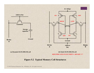
Static RAM (SRAM) cell Figure 5.2 Typical Memory Cell Structures (a) Dynamic RAM (DRAM) cell Bit line B C1 T1 T2 T3 T5 T6 T4 C2 Bit line B Bit line B Transistor Ground Storage capacitor © 2016 Pearson Education, Inc., Hoboken, NJ. All rights reserved. HIGH LOW OFF OFF ON ON RED INDICATES STATE WHEN A BINARY “1”
7.
+ Static RAM (SRAM) Digital device
that uses the same logic elements used in the processor Binary values are stored using traditional flip-flop logic gate configurations Will hold its data as long as power is supplied to it © 2016 Pearson Education, Inc., Hoboken, NJ. All rights reserved.
8.
+ SRAM versus DRAM Both
volatile Power must be continuously supplied to the memory to preserve the bit values Dynamic cell Simpler to build, smaller More dense (smaller cells = more cells per unit area) Less expensive Requires the supporting refresh circuitry Tend to be favored for large memory requirements Used for main memory Static Faster Used for cache memory (both on and off chip) SRAM DRAM © 2016 Pearson Education, Inc., Hoboken, NJ. All rights reserved.
9.
+ Read Only Memory
(ROM) Contains a permanent pattern of data that cannot be changed or added to No power source is required to maintain the bit values in memory Data or program is permanently in main memory and never needs to be loaded from a secondary storage device Data is actually wired into the chip as part of the fabrication process Disadvantages of this: No room for error, if one bit is wrong the whole batch of ROMs must be thrown out Data insertion step includes a relatively large fixed cost © 2016 Pearson Education, Inc., Hoboken, NJ. All rights reserved.
10.
+ Programmable ROM (PROM) Less
expensive alternative Nonvolatile and may be written into only once Writing process is performed electrically and may be performed by supplier or customer at a time later than the original chip fabrication Special equipment is required for the writing process Provides flexibility and convenience Attractive for high volume production runs © 2016 Pearson Education, Inc., Hoboken, NJ. All rights reserved.
11.
Read-Mostly Memory EPROM Erasable programmable read-only
memory Erasure process can be performed repeatedly More expensive than PROM but it has the advantage of the multiple update capability EEPROM Electrically erasable programmable read-only memory Can be written into at any time without erasing prior contents Combines the advantage of non-volatility with the flexibility of being updatable in place More expensive than EPROM Flash Memory Intermediate between EPROM and EEPROM in both cost and functionality Uses an electrical erasing technology, does not provide byte-level erasure Microchip is organized so that a section of memory cells are erased in a single action or “flash” © 2016 Pearson Education, Inc., Hoboken, NJ. All rights reserved.
12.
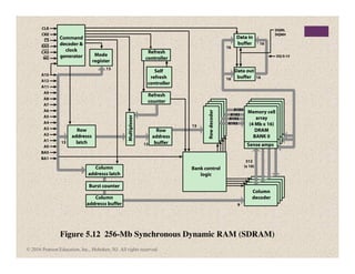
Column Decoder Refresh circuitry Memory
array (2048 2048 4) Row De- coder A0 A1 A10 Row Address Buffer Column Address Buffer Timing and Control RAS CAS WE OE MUX Refresh Counter Data Input Buffer Data Output Buffer D1 D2 D3 D4 Figure 5.3 Typical 16 Megabit DRAM (4M 4) © 2016 Pearson Education, Inc., Hoboken, NJ. All rights reserved. Organized as four square arrays of 2048 by 2048 elements. Elements of the array are connected by both horizontal (row) and vertical (column) lines. Horizontal line connects to the Select terminal of each cell in its row Vertical line connects to the Data-In/Sense terminal of each cell in its column. Refresh involves stepping through each row, reading the cells with RAS and then writing them right back.
13.
© 2016 Pearson
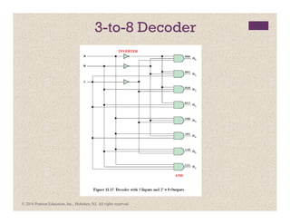
Education, Inc., Hoboken, NJ. All rights reserved. 3-to-8 Decoder INVERTER AND
14.
© 2016 Pearson
Education, Inc., Hoboken, NJ. All rights reserved. 4-Bit Multiplexer INVERTER AND OR F=D0+D1+D2+D3
15.
4M 4 24 Pin
Dip 0.6" Top View Figure 5.4 Typical Memory Package Pins and Signals 32 31 30 29 28 27 26 25 24 23 22 21 20 19 18 17 1 2 3 4 5 6 7 8 9 10 11 12 13 14 15 16 A19 A16 A15 A12 A7 A6 A5 A4 A3 A2 A1 A0 D0 D1 D2 Vss Vcc A18 A17 A14 A13 A8 A9 A11 Vpp A10 CE D7 D6 D5 D4 D3 32 Pin Dip 0.6" Top View 1M 8 24 23 22 21 20 19 18 17 16 15 14 13 1 2 3 4 5 6 7 8 9 10 11 12 Vcc D0 D1 WE RAS NC A10 A0 A1 A2 A3 Vcc Vss D3 D2 CAS OE A9 A8 A7 A6 A5 A4 Vss (a) 8 Mbit EPROM (b) 16 Mbit DRAM © 2016 Pearson Education, Inc., Hoboken, NJ. All rights reserved.
16.
512 words by 512
bits Chip #1 Memory buffer register (MBR) Figure 5.5 256-KByte Memory Organization Memory address register (MAR) Decode 1 of 512 bit-sense Decode 1 of 512 512 words by 512 bits Chip #8 Decode 1 of 512 bit-sense Decode 1 of 512 1 9 9 2 3 4 5 6 7 8 © 2016 Pearson Education, Inc., Hoboken, NJ. All rights reserved.
17.
+ © 2016 Pearson
Education, Inc., Hoboken, NJ. All rights reserved.
18.
Interleaved Memory Composed
of a collection of DRAM chips Grouped together to form a memory bank Each bank is independently able to service a memory read or write request K banks can service K requests simultaneously, increasing memory read or write rates by a factor of K If consecutive words of memory are stored in different banks, the transfer of a block of memory is speeded up © 2016 Pearson Education, Inc., Hoboken, NJ. All rights reserved.
19.
+ Error Correction Hard Failure Permanent
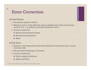
physical defect Memory cell or cells affected cannot reliably store data but become stuck at 0 or 1 or switch erratically between 0 and 1 Can be caused by: Harsh environmental abuse Manufacturing defects Wear Soft Error Random, non-destructive event that alters the contents of one or more memory cells No permanent damage to memory Can be caused by: Power supply problems Alpha particles © 2016 Pearson Education, Inc., Hoboken, NJ. All rights reserved.
20.
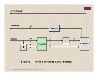
f f Compare Corrector Memory Figure 5.7 Error-Correcting
Code Function Data In Data Out Error Signal M K M M K K © 2016 Pearson Education, Inc., Hoboken, NJ. All rights reserved.
21.
1 1 1 0 0 0 (d) (c) 0 1 1 1 0 0 0 0 Figure
5.8 Hamming Error-Correcting Code 1 1 1 0 0 1 (b) (a) 0 1 A B C A B C A B C A B C 1 0 1 © 2016 Pearson Education, Inc., Hoboken, NJ. All rights reserved.
22.
Single-Error Correction Single-Error
Correction/ Double-Error Detection Data Bits Check Bits % Increase Check Bits % Increase 8 4 50 5 62.5 16 5 31.25 6 37.5 32 6 18.75 7 21.875 64 7 10.94 8 12.5 128 8 6.25 9 7.03 256 9 3.52 10 3.91 Table 5.2 Increase in Word Length with Error Correction © 2016 Pearson Education, Inc., Hoboken, NJ. All rights reserved.
23.
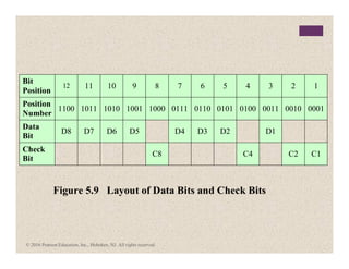
Bit Position 12 11 10
9 8 7 6 5 4 3 2 1 Position Number 1100 1011 1010 1001 1000 0111 0110 0101 0100 0011 0010 0001 Data Bit D8 D7 D6 D5 D4 D3 D2 D1 Check Bit C8 C4 C2 C1 Figure 5.9 Layout of Data Bits and Check Bits © 2016 Pearson Education, Inc., Hoboken, NJ. All rights reserved.
24.
© 2016 Pearson
Education, Inc., Hoboken, NJ. All rights reserved. C1 = D1 D2 D4 D5 D7 C2 = D1 D3 D4 D6 D7 C4 = D2 D3 D4 D8 C8 = D5 D6 D7 D8 Hamming Codes - SEC
25.
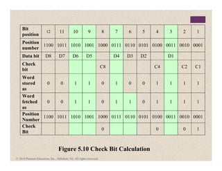
Bit position 12 11 10
9 8 7 6 5 4 3 2 1 Position number 1100 1011 1010 1001 1000 0111 0110 0101 0100 0011 0010 0001 Data bit D8 D7 D6 D5 D4 D3 D2 D1 Check bit C8 C4 C2 C1 Word stored as 0 0 1 1 0 1 0 0 1 1 1 1 Word fetched as 0 0 1 1 0 1 1 0 1 1 1 1 Position Number 1100 1011 1010 1001 1000 0111 0110 0101 0100 0011 0010 0001 Check Bit 0 0 0 1 Figure 5.10 Check Bit Calculation © 2016 Pearson Education, Inc., Hoboken, NJ. All rights reserved.
26.
1 0 0 1 1 1 (e) (d) 0 Figure 5.11
Hamming SEC-DED Code 0 0 1 1 0 1 (b) (a) 0 0 1 0 1 1 1 1 1 1 1 0 0 1 1 1 (f) 0 1 0 0 1 0 1 (c) 0 1 0 0 1 0 1 0 © 2016 Pearson Education, Inc., Hoboken, NJ. All rights reserved.
27.
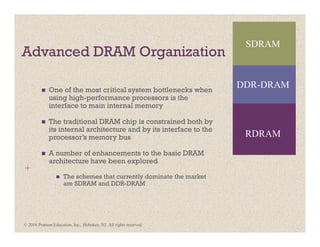
+ Advanced DRAM Organization One
of the most critical system bottlenecks when using high-performance processors is the interface to main internal memory The traditional DRAM chip is constrained both by its internal architecture and by its interface to the processor’s memory bus A number of enhancements to the basic DRAM architecture have been explored The schemes that currently dominate the market are SDRAM and DDR-DRAM SDRAM RDRAM DDR-DRAM © 2016 Pearson Education, Inc., Hoboken, NJ. All rights reserved.
28.
Synchronous DRAM (SDRAM) One
of the most widely used forms of DRAM Exchanges data with the processor synchronized to an external clock signal and running at the full speed of the processor/memory bus without imposing wait states Exchanges data with the processor synchronized to an external clock signal and running at the full speed of the processor/memory bus without imposing wait states With synchronous access the DRAM moves data in and out under control of the system clock • The processor or other master issues the instruction and address information which is latched by the DRAM • The DRAM then responds after a set number of clock cycles • Meanwhile the master can safely do other tasks while the SDRAM is processing © 2016 Pearson Education, Inc., Hoboken, NJ. All rights reserved.
29.
© 2016 Pearson
Education, Inc., Hoboken, NJ. All rights reserved.
30.
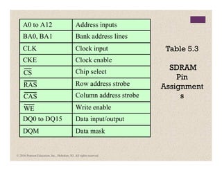
Table 5.3 SDRAM Pin Assignment s A0 to
A12 Address inputs BA0, BA1 Bank address lines CLK Clock input CKE Clock enable CS Chip select RAS Row address strobe CAS Column address strobe WE Write enable DQ0 to DQ15 Data input/output DQM Data mask © 2016 Pearson Education, Inc., Hoboken, NJ. All rights reserved.
31.
T0 CLK COMMAND Figure 5.13 SDRAM
Read Timing (Burst Length = 4, CAS latency = 2) DQs T1 T2 T3 T4 T5 T6 T7 T8 DOUT A0 DOUT A1 DOUT A2 DOUT A3 READ A NOP NOP NOP NOP NOP NOP NOP NOP © 2016 Pearson Education, Inc., Hoboken, NJ. All rights reserved.
32.
+ Double Data Rate
SDRAM (DDR SDRAM) Developed by the JEDEC Solid State Technology Association (Electronic Industries Alliance’s semiconductor-engineering- standardization body) Numerous companies make DDR chips, which are widely used in desktop computers and servers DDR achieves higher data rates in three ways: First, the data transfer is synchronized to both the rising and falling edge of the clock, rather than just the rising edge Second, DDR uses higher clock rate on the bus to increase the transfer rate Third, a buffering scheme is used © 2016 Pearson Education, Inc., Hoboken, NJ. All rights reserved.
33.
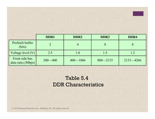
DDR1 DDR2 DDR3
DDR4 Prefetch buffer (bits) 2 4 8 8 Voltage level (V) 2.5 1.8 1.5 1.2 Front side bus data rates (Mbps) 200—400 400—1066 800—2133 2133—4266 Table 5.4 DDR Characteristics © 2016 Pearson Education, Inc., Hoboken, NJ. All rights reserved.
34.
© 2016 Pearson
Education, Inc., Hoboken, NJ. All rights reserved.
35.
© 2016 Pearson
Education, Inc., Hoboken, NJ. All rights reserved.
36.
© 2016 Pearson
Education, Inc., Hoboken, NJ. All rights reserved.
37.
© 2016 Pearson
Education, Inc., Hoboken, NJ. All rights reserved.
38.
© 2016 Pearson
Education, Inc., Hoboken, NJ. All rights reserved.
39.
© 2016 Pearson
Education, Inc., Hoboken, NJ. All rights reserved.
40.
+ Flash Memory Used both
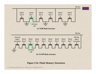
for internal memory and external memory applications First introduced in the mid-1980’s Is intermediate between EPROM and EEPROM in both cost and functionality Uses an electrical erasing technology like EEPROM It is possible to erase just blocks of memory rather than an entire chip Gets its name because the microchip is organized so that a section of memory cells are erased in a single action Does not provide byte-level erasure Uses only one transistor per bit so it achieves the high density of EPROM © 2016 Pearson Education, Inc., Hoboken, NJ. All rights reserved.
41.
Figure 5.15 Flash
Memory Operation (a) Transistor structure (b) Flash memory cell in one state (c) Flash memory cell in zero state Control Gate N+ Drain N+ Source P-substrate Control Gate N+ Drain N+ Source Floating Gate P-substrate Control Gate + + + + + + N+ Drain N+ Source P-substrate – – – – – – © 2016 Pearson Education, Inc., Hoboken, NJ. All rights reserved.
42.
© 2016 Pearson
Education, Inc., Hoboken, NJ. All rights reserved.
43.
(a) NOR Figure 5.17
Kiviat Graphs for Flash Memory Cost per bit File storage use Code execution Capacity Write speed Read speed Active power Low Low Low Easy Easy Standby power High High High High High High Hard Hard Low Low Low (b) NAND Cost per bit File storage use Code execution Capacity Write speed Read speed Active power Low Low Low Easy Easy Standby power High High High High High High Hard Hard Low Low Low © 2016 Pearson Education, Inc., Hoboken, NJ. All rights reserved.
44.
Figure 5.18 Nonvolatile
RAM within the Memory Hierarchy SRAM STT-RAM PCRAM ReRAM Increasing performance and endurance Decreasing cost per bit, increasing capacity or density DRAM NAND FLASH HARD DISK © 2016 Pearson Education, Inc., Hoboken, NJ. All rights reserved.
45.
Figure 5.19 Nonvolatile
RAM Technologies (a) STT-RAM (b) PCRAM Bit line Free layer Reference layer Base electrode Interface layer Direction of magnetization Electric current binary 0 Interface layer Insulating layer Perpendicular magnetic layer Perpendicular magnetic layer Bit line Free layer Reference layer Base electrode Interface layer Direction of magnetization Electric current binary 1 Interface layer Insulating layer Perpendicular magnetic layer Perpendicular magnetic layer Top electrode Bottom electrode Polycrystaline chalcogenide Heater Insulator Filament Metal oxide Insulator Metal oxide Insulator (c) ReRAM Top electrode Bottom electrode Filament Oxidation: high resistance Reduction: low resistance Top electrode Bottom electrode Top electrode Bottom electrode Polycrystaline chalcogenide Amorphous chalcogenide Heater Insulator © 2016 Pearson Education, Inc., Hoboken, NJ. All rights reserved.
46.
+ Summary Semiconductor main
memory Organization DRAM and SRAM Types of ROM Chip logic Chip packaging Module organization Interleaved memory Error correction DDR DRAM Synchronous DRAM DDR SDRAM Flash memory Operation NOR and NAND flash memory Newer nonvolatile solid-state memory technologies Chapter 5 Internal Memory © 2016 Pearson Education, Inc., Hoboken, NJ. All rights reserved.
Download