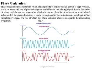
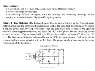
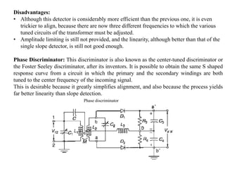
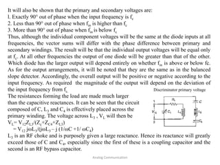
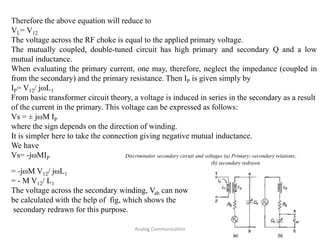
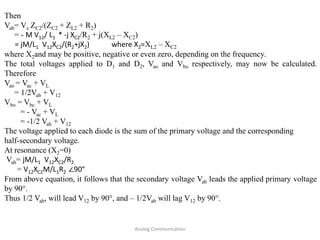
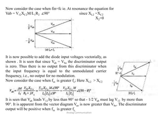
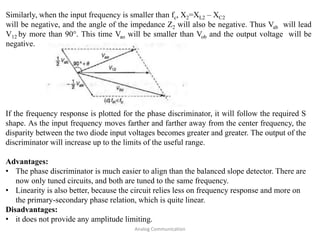
The document covers the principles of angle modulation in analog communication, focusing on frequency modulation (FM) and phase modulation (PM) signals, their mathematical representations, and the relationship between modulation techniques and signal characteristics. It details the generation, implementation, and key parameters of FM and PM systems, including deviation ratios and modulation indices, as well as problem-solving examples involving these concepts. Additionally, it discusses methods for generating FM and PM through direct and indirect means.
![Analog Communication
Semester V[ETC/ECE 5.6]
Analog Communication](https://image.slidesharecdn.com/anglemodulationunit2-240724093851-fbf588ee/85/Angle-Modulation-Frequency-Modulation-and-Phase-Modulation-pptx-1-320.jpg)
![Analog Communication
Semester V[ETC/ECE 5.6]
Analog Communication](https://image.slidesharecdn.com/anglemodulationunit2-240724093851-fbf588ee/75/Angle-Modulation-Frequency-Modulation-and-Phase-Modulation-pptx-1-2048.jpg)
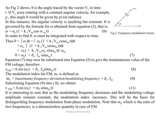
![Analog Communication
Mathematical Representation of FM:
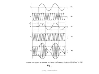
From Fig.1.c , it is seen that the instantaneous frequency of the frequency modulated wave is
given by
f = fc( 1+ k f Vmcos ωm t ) (2)
where fc is unmodulated (or average) carrier frequency,
k f is proportionality constant expressed in Hz/volt
Vmcosωm t is instantaneous modulating voltage.
The maximum deviation for this signal will occur when the cosine term, has its maximum
value, ± 1. Under these conditions, the instantaneous frequency will be
f = fc (1 ± k f Vm) , (3)
so that the maximum deviation 𝛿f will be given by
𝛿f = k f Vm fc (4)
The instantaneous amplitude of the FM signal will be given by a formula of the form
vFM=Asin[f(ωc ,ωm )] =Asinθ (5)
where f(ωc , ωm ) is some function of the carrier and modulating frequencies. This function
represents an angle and will be called θ for convenience.](https://image.slidesharecdn.com/anglemodulationunit2-240724093851-fbf588ee/85/Angle-Modulation-Frequency-Modulation-and-Phase-Modulation-pptx-6-320.jpg)