Am modulator and demodulator for school project.pptx
1.
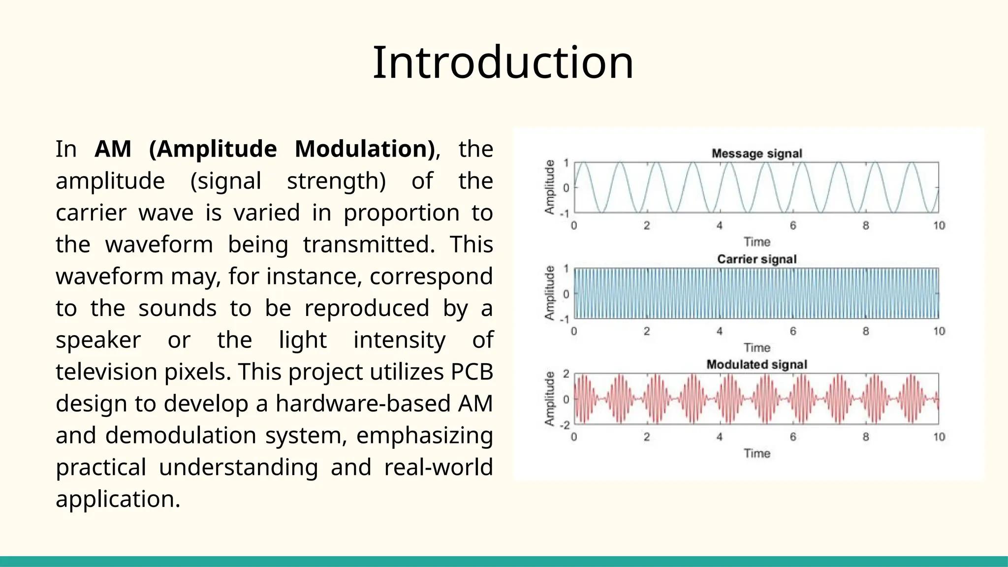
In AM (AmplitudeModulation), the
amplitude (signal strength) of the
carrier wave is varied in proportion to
the waveform being transmitted. This
waveform may, for instance, correspond
to the sounds to be reproduced by a
speaker or the light intensity of
television pixels. This project utilizes PCB
design to develop a hardware-based AM
and demodulation system, emphasizing
practical understanding and real-world
application.
Introduction
2.
Objectives:
1. Design andfabricate a PCB for Amplitude modulation and
demodulation.
2. Perform etching, soldering, and connection testing.
3. Establish reliable connections and verify them
4. Modulate a carrier signal with an analogue input.
5. Recover the original signal via demodulation.
6. Ensure high efficiency and minimal distortion.
3.
Printed Circuit Board
1.Two Single Layer Copper Clad
Boards
2. FeCl3 solution (for etching)
3. One Hand Saw
4. Mini Drill Machine
5. Soldering Iron
6. Lead Solder
7. Nail Polish and Remover (for
drawing the circuit)
Apparatus
Methodology
1. Circuit Design:Draft and verify schematics.
2. PCB Design: Manually draw circuit layout.
3. Etching: Use FeCl3 solution to remove excess copper.
4. Component Assembly: Solder components onto PCB.
5. Connection Checking: Verify continuity using
multimeter.
6. Testing: Test modulation and demodulation using
input signals.
7.
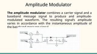
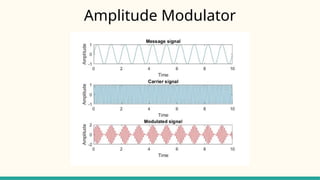
Amplitude Modulator
The amplitudemodulator combines a carrier signal and a
baseband message signal to produce and amplitude-
modulated waveform. The resulting signal’s amplitude
varies in accordance with the instantaneous amplitude of
the baseband message signal
8.
Amplitude Modulator
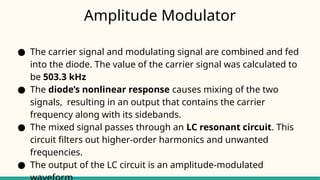
● Thecarrier signal and modulating signal are combined and fed
into the diode. The value of the carrier signal was calculated to
be 503.3 kHz
● The diode’s nonlinear response causes mixing of the two
signals, resulting in an output that contains the carrier
frequency along with its sidebands.
● The mixed signal passes through an LC resonant circuit. This
circuit filters out higher-order harmonics and unwanted
frequencies.
● The output of the LC circuit is an amplitude-modulated
Amplitude Modulator
Problems DuringImplementation:
● Carrier Leakage: The carrier signal appeared in the output
without proper modulation. This was mainly due to a poor
balance in the modulator circuit and mismatched
components. To solve this, we correctly calculated the carrier
frequency and used the right components.
● Noise and interference: High-frequency noise or external
interference distorted the modulated signal. To solve this, we
properly grounded the PCB.
11.
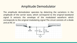
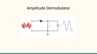
Amplitude Demodulator
The amplitudedemodulator operates by detecting the variations in the
amplitude of the carrier wave, which correspond to the original baseband
signal It extracts the envelope of the modulated waveform which
corresponds to the original modulating signal The circuit consists of a diode
and an RC circuit component
12.
Amplitude Demodulator
● TheAM signal is applied to the diode, which rectifies the signal,
producing a waveform where only the positive peaks of the
carrier wave remain.
● The rectified signal is passed through the RC low-pass filter. The
capacitor in this circuit smooths the rapid variations, and the
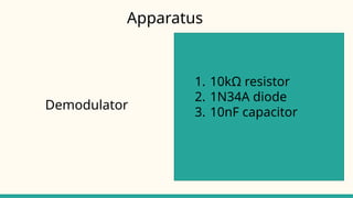
resistor determines the cutoff frequency. We used a 10nF
Capacitor and a 10kΩ resistor. So, the cutoff frequency is 1.5 kHz.
● The smooth signal still contains a DC offset from before. A
capacitor in series removes this offset, leaving only the baseband
signal.
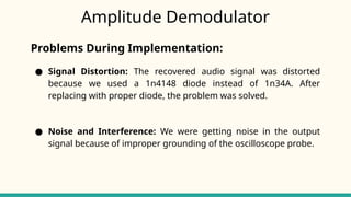
Amplitude Demodulator
Problems DuringImplementation:
● Signal Distortion: The recovered audio signal was distorted
because we used a 1n4148 diode instead of 1n34A. After
replacing with proper diode, the problem was solved.
● Noise and Interference: We were getting noise in the output
signal because of improper grounding of the oscilloscope probe.