Recommended

Recommended
More Related Content
What's hot
What's hot (20)
Similar to A Wide Band Low-Power Variable Gain Lna for Multi-Standard Applications
Similar to A Wide Band Low-Power Variable Gain Lna for Multi-Standard Applications (20)
More from RFIC-IUMA
More from RFIC-IUMA (20)
Recently uploaded
Recently uploaded (20)
A Wide Band Low-Power Variable Gain Lna for Multi-Standard Applications
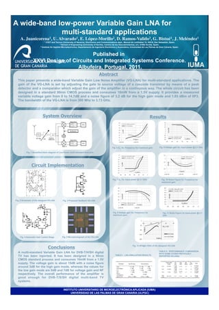
- 1. A wide-band low-power Variable Gain LNA for multi-standard applications A. Juanicorena1, U. Alvarado1, E. López-Morillo2, D. Ramos-Valido3, G. Bistué1, J. Meléndez1 1 1CEIT and Tecnun (University of Navarra), Electronics and Communications dept., Manuel de Lardizábal 15, 20018, San Sebastián, Spain. 2 School of Engineering (University of Sevilla), Camino de los Descubrimientos, s/n, 41092 Sevilla, Spain. 3 Institute for Applied Microelectronics, Departamento de Ingeniería Electrónica y Automática, Universidad de Las Palmas de Gran Canaria, Spain. Published in XXVI Design of Circuits and Integrated Systems Conference. Albufeira, Portugal, 2011. Abstract This paper presents a wide-band Variable Gain Low Noise Amplifier (VG-LNA) for multi-standard applications. The gain of the VG-LNA is set by adjusting the gate to source voltage of a cascode transistor by means of a peak detector and a comparator which adjust the gain of the amplifier in a continuous way. The whole circuit has been designed in a standard 90nm CMOS process and consumes 10mW from a 1.5V supply. It provides a measured variable voltage gain from 0 to 14.7dB and a noise figure of 3.2 dB for the high gain mode and 1.85 dBm of IIP3. The bandwidth of the VG-LNA is from 300 Mhz to 3.73 GHz. System Overview Results 0 Fig. 6 S11 Vs. Frequency for maximum gain Fig. 9 Voltage gain Vs. Input power @ 2.1 GHz Fig. 1 Simplified block diagram of Low-Power multi-standard front-end. Circuit Implementation Fig. 7 S11 Vs. Input power @ 2.1 GHz Fig. 10 Noise Figure Vs. Frequency for maximum gain 0 Fig. 2 Schematic of the designed VG-LNA Fig. 3 Proposed feedback VG-LNA Fig. 8 Voltage gain Vs. Frequency for Fig. 11 Noise Figure Vs.input power @ 2.1 maximum gain. GHz Fig. 4 Automatic Gain Control Stage Fig. 5 Microphotograph of the VG-LNA Conclusions Fig. 12 IIP3@2.1GHz of the designed VG-LNA TABLE II. PERFORMANCE COMPARISON A multi-standard Variable Gain LNA for DVB-T/H/SH digital WITH SOME OTHER PREVIOUSLY TABLE I. LNA SIMULATION RESULTS TV has been reported. It has been designed in a 90nm REPORTED VG-LNAs CMOS standard process and consumes 10mW from a 1.5V supply. The voltage gain is about 15dB with a noise figure around 3dB for the high gain mode, whereas the values for the low gain mode are 0dB and 7dB for voltage gain and NF respectively. The overall performance of the amplifier is good enough for DVB-T/S/SH digital multi-band TV systems. INSTITUTO UNIVERSITARIO DE MICROELECTRÓNICA APLICADA (IUMA) UNIVERSIDAD DE LAS PALMAS DE GRAN CANARIA (ULPGC)