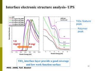
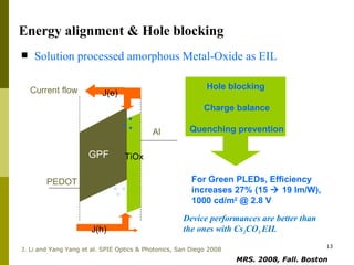
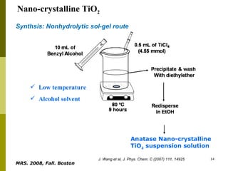
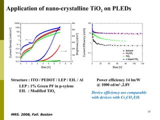
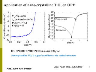
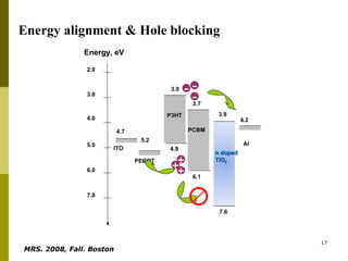
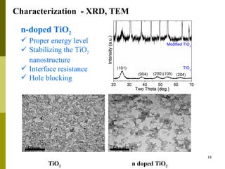
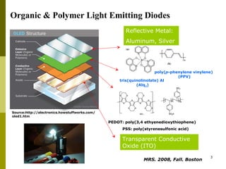
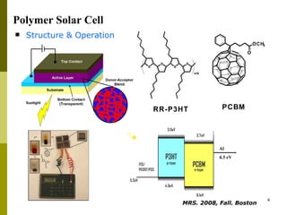
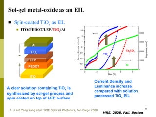
The Application of Titanium Oxide on Organic Optoelectronic Devices by Sol-Gel Process   Juo-hao Li, MiHyae Park and Yang Yang Department of Materials Science and Engineering University of California – Los Angeles, California MRS. 2008, Fall. Boston
Outline Introduction / Motivation Printed electronics & solution process Amorphous titanium oxide  Solution processed electron injection layer  PLEDs using TiO X  as the ETL Nano-crystalline titanium oxide Sol-gel processed Nano-crystalline TiO 2   The application on PLEDs & Organic Solar Cell Summary MRS. 2008, Fall. Boston
Organic & Polymer Light Emitting Diodes Source:http://electronics.howstuffworks.com/oled1.htm Reflective Metal: Aluminum, Silver tris(quinolinolate) Al (Alq 3 ) poly( p -phenylene vinylene)  (PPV) PSS: poly(styrenesulfonic acid) PEDOT: poly(3,4 ethyenedioxythiophene) Transparent Conductive Oxide (ITO) MRS. 2008, Fall. Boston
Polymer Solar Cell Structure & Operation Al 4.3 eV RR-P3HT PCBM MRS. 2008, Fall. Boston
Roll to Roll process Printing Process Inkjej printing Ink-transfer Printed electronics & solution process Franky So, Junji Kido, and Paul Burrows, MRS BULLETIN • VOLUME 33 • JULY 2008 Low cost High throughput Flexible M. BERGGREN, D. NILSSON AND N. D. ROBINSON, nature materials, 6, p1-5, 2007 MRS. 2008, Fall. Boston
Solution processed interfacial layer OLEDs architecture & charge injection layer Cathode HIL/HTL Anode/ Substrate Emissive layer - + EIL/ETL - + - - + + Increase injection and luminance efficiency  Reduce the barrier energy Help charge transport Avoid the quenching effect Quantum confinement Charge injection & Charge balance MRS. 2008, Fall. Boston   + -
Challenges of solution processed interfacial layer Thin film deposition Easy processing & comparability with other organic layer Energy level alignment  Quantum confinement Thickness control Charge balance Interface morphology  Stability Thermal stability & degradation MRS. 2008, Fall. Boston
Spin-coated Cs 2 CO 3  as EIL   ITO/PEDOT/LEP/ Cs 2 CO 3 /Al ITO PEDOT LEP Al  Cs 2 CO 3 + - The solvent used to dissolve Cs 2 CO 3  would not wash out the underneath LEP layer all solution process J. Huang et al.  Adv. Funct. Mater. 2007, 17, 1966–1973 Cs 2 CO 3  (Sol.) Cs 2 CO 3  (Evap.) Cs/Al Solution Processed Cs 2 CO 3  layer MRS. 2008, Fall. Boston
Spin-coated TiO x  as EIL   ITO/PEDOT/LEP/ TiO x /Al Sol-gel metal-oxide as an EIL ITO PEDOT LEP Al  TiO x + - Current Density and Luminance increase compared with solution processed TiO x  EIL   A clear solution containing TiO X  is synthesized by sol-gel process and spin coated on top of LEP surface   J. Li and Yang Yang et al.  SPIE Optics & Photonics, San Diego 2008 MRS. 2008, Fall. Boston
Charge injection ability Photovoltaic measurement – Built-in potential   Devices with TiO x  EIL have similar built-in potential compared with the devices with Ca & Cs 2 CO 3  layer Low injection barrier High current density MRS. 2008, Fall. Boston
Concentration  dependence 2.97 6.04 17.3 6.4 1.0 mg/ml * Measured at the brightness of 1000 cd/m 2 13.52 18.98 3.67 Power Efficiency* [lm/W] 14.21 7.76 3.3 0.5 mg/ml 16.92 6.27 2.8 0.2 mg/ml 5.84 16.67 5.0 0.1 mg/ml Current* efficiency [cd/A]  J* [mA/cm 2 ] Volt* [V] TiO X Conc.
Interface electronic structure analysis- UPS TiO X  interface layer provide a good coverage and low work function surface 0 mg/ml 1.0 mg/ml TiOx feature peak Polymer peak MRS. 2008, Fall. Boston
Solution processed amorphous Metal-Oxide as EIL GPF TiOx J(h) J(e) PEDOT Al ● ○ ○ ○ ● ● Current flow For Green PLEDs, Efficiency increases 27% (15    19 lm/W), 1000 cd/m 2  @ 2.8 V  Hole blocking  Charge balance Quenching prevention J. Li and Yang Yang et al.  SPIE Optics & Photonics, San Diego 2008 Energy alignment & Hole blocking MRS. 2008, Fall. Boston   Device performances are better than  the ones with Cs 2 CO 3  EIL
Nano - crystalline TiO 2 J. Wang et al, J. Phys. Chem. C (2007) 111, 14925 Synthsis:  Nonhydrolytic sol-gel route  Low temperature Alcohol solvent Anatase Nano-crystalline TiO 2  suspension solution MRS. 2008, Fall. Boston
Structure : ITO / PEDOT / LEP / EIL / Al LEP : 1% Green PF in p-xylene EIL  : Modified TiO 2   Application of nano-crystalline  TiO 2  on PLEDs Device efficiency are comparable  with devices with Cs 2 CO 3  EIL Power efficiency 14 lm/W @ 1000 cd/m 2,  ,2.8V MRS. 2008, Fall. Boston
Nanocrystalline TiO 2   is a good candidate as the cathode structure Application of nano - crystalline  TiO 2  on OPV V oc  (V) = 0.58 J sc  (mA/cm 2 ) = 10.76 PCE (%) = 4.2 FF(%) = 67 ITO / PEDOT / P3HT:PCBM/n doped TiO 2 / Al MRS. 2008, Fall. Boston   Adv. Funt. Mat. submitted
Energy alignment & Hole blocking - - - + + + MRS. 2008, Fall. Boston   Energy, eV PCBM 4.9 3.7 6.1 PEDOT ITO 5.2 4.7 n doped TiO 2 3.9 7.6 4.2 Al 4.0 2.0 7.0 6.0 5.0 3.0 P3HT 3.0
Characterization  -  XRD,  TEM   n-doped TiO 2 Proper energy level Stabilizing the TiO 2  nanostructure Interface resistance Hole blocking TiO 2 n doped  TiO 2 50nm 50nm
Summary Solution processed   interfacial layer  can be applied in the process of  printed electronics  and act as charge injection layer to improve the interface and device performance  Sol-gel  processed  amorphous titanium oxide  is demonstrated to be a good electron injection layer used for efficient PLEDs.  Sol-gel processed  nano-crystalline titanium oxide  can be employed as the EIL in both OPV and PLEDs  MRS. 2008, Fall. Boston
Prof. Yang Yang’s gourp members Dr.  Jianhui Hou , Solarmer Inc. Funding Agencies, CDA, Air Fource, ONR, NSF Acknowledgement Thank you for your attention MRS. 2008, Fall. Boston

Mrs 2008 Fall Walker

  • 1.
    The Application ofTitanium Oxide on Organic Optoelectronic Devices by Sol-Gel Process Juo-hao Li, MiHyae Park and Yang Yang Department of Materials Science and Engineering University of California – Los Angeles, California MRS. 2008, Fall. Boston
  • 2.
    Outline Introduction /Motivation Printed electronics & solution process Amorphous titanium oxide Solution processed electron injection layer PLEDs using TiO X as the ETL Nano-crystalline titanium oxide Sol-gel processed Nano-crystalline TiO 2 The application on PLEDs & Organic Solar Cell Summary MRS. 2008, Fall. Boston
  • 3.
    Organic & PolymerLight Emitting Diodes Source:http://electronics.howstuffworks.com/oled1.htm Reflective Metal: Aluminum, Silver tris(quinolinolate) Al (Alq 3 ) poly( p -phenylene vinylene) (PPV) PSS: poly(styrenesulfonic acid) PEDOT: poly(3,4 ethyenedioxythiophene) Transparent Conductive Oxide (ITO) MRS. 2008, Fall. Boston
  • 4.
    Polymer Solar CellStructure & Operation Al 4.3 eV RR-P3HT PCBM MRS. 2008, Fall. Boston
  • 5.
    Roll to Rollprocess Printing Process Inkjej printing Ink-transfer Printed electronics & solution process Franky So, Junji Kido, and Paul Burrows, MRS BULLETIN • VOLUME 33 • JULY 2008 Low cost High throughput Flexible M. BERGGREN, D. NILSSON AND N. D. ROBINSON, nature materials, 6, p1-5, 2007 MRS. 2008, Fall. Boston
  • 6.
    Solution processed interfaciallayer OLEDs architecture & charge injection layer Cathode HIL/HTL Anode/ Substrate Emissive layer - + EIL/ETL - + - - + + Increase injection and luminance efficiency Reduce the barrier energy Help charge transport Avoid the quenching effect Quantum confinement Charge injection & Charge balance MRS. 2008, Fall. Boston + -
  • 7.
    Challenges of solutionprocessed interfacial layer Thin film deposition Easy processing & comparability with other organic layer Energy level alignment Quantum confinement Thickness control Charge balance Interface morphology Stability Thermal stability & degradation MRS. 2008, Fall. Boston
  • 8.
    Spin-coated Cs 2CO 3 as EIL ITO/PEDOT/LEP/ Cs 2 CO 3 /Al ITO PEDOT LEP Al Cs 2 CO 3 + - The solvent used to dissolve Cs 2 CO 3 would not wash out the underneath LEP layer all solution process J. Huang et al. Adv. Funct. Mater. 2007, 17, 1966–1973 Cs 2 CO 3 (Sol.) Cs 2 CO 3 (Evap.) Cs/Al Solution Processed Cs 2 CO 3 layer MRS. 2008, Fall. Boston
  • 9.
    Spin-coated TiO x as EIL ITO/PEDOT/LEP/ TiO x /Al Sol-gel metal-oxide as an EIL ITO PEDOT LEP Al TiO x + - Current Density and Luminance increase compared with solution processed TiO x EIL A clear solution containing TiO X is synthesized by sol-gel process and spin coated on top of LEP surface J. Li and Yang Yang et al. SPIE Optics & Photonics, San Diego 2008 MRS. 2008, Fall. Boston
  • 10.
    Charge injection abilityPhotovoltaic measurement – Built-in potential Devices with TiO x EIL have similar built-in potential compared with the devices with Ca & Cs 2 CO 3 layer Low injection barrier High current density MRS. 2008, Fall. Boston
  • 11.
    Concentration dependence2.97 6.04 17.3 6.4 1.0 mg/ml * Measured at the brightness of 1000 cd/m 2 13.52 18.98 3.67 Power Efficiency* [lm/W] 14.21 7.76 3.3 0.5 mg/ml 16.92 6.27 2.8 0.2 mg/ml 5.84 16.67 5.0 0.1 mg/ml Current* efficiency [cd/A] J* [mA/cm 2 ] Volt* [V] TiO X Conc.
  • 12.
    Interface electronic structureanalysis- UPS TiO X interface layer provide a good coverage and low work function surface 0 mg/ml 1.0 mg/ml TiOx feature peak Polymer peak MRS. 2008, Fall. Boston
  • 13.
    Solution processed amorphousMetal-Oxide as EIL GPF TiOx J(h) J(e) PEDOT Al ● ○ ○ ○ ● ● Current flow For Green PLEDs, Efficiency increases 27% (15  19 lm/W), 1000 cd/m 2 @ 2.8 V Hole blocking Charge balance Quenching prevention J. Li and Yang Yang et al. SPIE Optics & Photonics, San Diego 2008 Energy alignment & Hole blocking MRS. 2008, Fall. Boston Device performances are better than the ones with Cs 2 CO 3 EIL
  • 14.
    Nano - crystallineTiO 2 J. Wang et al, J. Phys. Chem. C (2007) 111, 14925 Synthsis: Nonhydrolytic sol-gel route Low temperature Alcohol solvent Anatase Nano-crystalline TiO 2 suspension solution MRS. 2008, Fall. Boston
  • 15.
    Structure : ITO/ PEDOT / LEP / EIL / Al LEP : 1% Green PF in p-xylene EIL : Modified TiO 2 Application of nano-crystalline TiO 2 on PLEDs Device efficiency are comparable with devices with Cs 2 CO 3 EIL Power efficiency 14 lm/W @ 1000 cd/m 2, ,2.8V MRS. 2008, Fall. Boston
  • 16.
    Nanocrystalline TiO 2 is a good candidate as the cathode structure Application of nano - crystalline TiO 2 on OPV V oc (V) = 0.58 J sc (mA/cm 2 ) = 10.76 PCE (%) = 4.2 FF(%) = 67 ITO / PEDOT / P3HT:PCBM/n doped TiO 2 / Al MRS. 2008, Fall. Boston Adv. Funt. Mat. submitted
  • 17.
    Energy alignment &Hole blocking - - - + + + MRS. 2008, Fall. Boston Energy, eV PCBM 4.9 3.7 6.1 PEDOT ITO 5.2 4.7 n doped TiO 2 3.9 7.6 4.2 Al 4.0 2.0 7.0 6.0 5.0 3.0 P3HT 3.0
  • 18.
    Characterization - XRD, TEM n-doped TiO 2 Proper energy level Stabilizing the TiO 2 nanostructure Interface resistance Hole blocking TiO 2 n doped TiO 2 50nm 50nm
  • 19.
    Summary Solution processed interfacial layer can be applied in the process of printed electronics and act as charge injection layer to improve the interface and device performance Sol-gel processed amorphous titanium oxide is demonstrated to be a good electron injection layer used for efficient PLEDs. Sol-gel processed nano-crystalline titanium oxide can be employed as the EIL in both OPV and PLEDs MRS. 2008, Fall. Boston
  • 20.
    Prof. Yang Yang’sgourp members Dr. Jianhui Hou , Solarmer Inc. Funding Agencies, CDA, Air Fource, ONR, NSF Acknowledgement Thank you for your attention MRS. 2008, Fall. Boston