
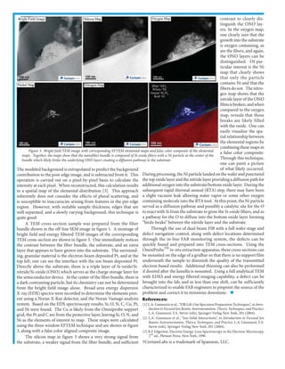
The document describes using transmission electron microscopy (TEM) and energy-filtered transmission electron microscopy (EFTEM) to characterize nanofiber bundles detected as defects in a semiconductor fabrication facility (FAB). A dual-beam focused ion beam was used to prepare a TEM cross-section sample of one of the fiber bundles. EFTEM elemental mapping revealed that the fibers are composed of silicon oxide and originate from a nickel particle, which likely broke the underlying silicon oxide-silicon nitride-silicon oxide layers during processing, providing a pathway for oxygen diffusion and fiber growth. The technique allows pinpointing the source of defects to minimize downtime in the FAB.