SlideShare a Scribd company logo
1 of 16
Download to read offline
Cloud IT Solution Page 424
Logic gate
Logic gates are the basic building blocks of any digital system. It is an electronic circuit
having one or more than one input and only one output.
Types
 AND Gate
 OR Gate
 NOT Gate
 NAND Gate
 NOR Gate
 XOR Gate
AND Gate
A circuit which performs an AND operation is shown in figure. It has n input (n >= 2) and
one output.
 Logic diagram
Truth Table
Digital Logic Circuit
Cloud IT Solution Page 425
OR Gate
A circuit which performs an OR operation is shown in figure. It has n input (n >= 2) and one
output.
Logic diagram
Truth Table
NOT Gate
NOT gate is also known as Inverter. It has one input A and one output Y.
 Logic diagram
Cloud IT Solution Page 426
Truth Table
NAND Gate
A NOT-AND operation is known as NAND operation. It has n input (n >= 2) and one output.
Logic diagram
Truth Table
NOR Gate
A NOT-OR operation is known as NOR operation. It has n input (n >= 2) and one output.
Cloud IT Solution Page 427
Logic diagram
Truth Table
XOR Gate
XOR or Ex-OR gate is a special type of gate. It can be used in the half adder, full adder and
subtractor. The exclusive-OR gate is abbreviated as EX-OR gate or sometime as X-OR gate.
It has n input (n >= 2) and one output.
Logic diagram
Truth Table
Cloud IT Solution Page 428
XNOR Gate
XNOR gate is a special type of gate. It can be used in the half adder, full adder and subtractor.
The exclusive-NOR gate is abbreviated as EX-NOR gate or sometime as X-NOR gate. It has
n input (n >= 2) and one output
Logic diagram
Truth Table
NAND and NOR Universal Gate
 NAND and NOR are called universal gates because all the other gates like
and,or,not,xor and xnor can be derived from it.
 Any basic gate can be implemented using NAND and NOR.
Cloud IT Solution Page 429
De Morgan's Theorems
 De Morgan has suggested two theorems which are extremely useful in
Boolean Algebra.
Theorem 1
 The left hand side (LHS) of this theorem represents a NAND gate with inputs A and
B, whereas the right hand side (RHS) of the theorem represents an OR gate with
inverted inputs.
Cloud IT Solution Page 430
This OR gate is called as Bubbled OR.
Table showing verification of the De Morgan's first theorem –
Theorem 2
The LHS of this theorem represents a NOR gate with inputs A and B, whereas the RHS
represents an AND gate with inverted inputs.
Cloud IT Solution Page 431
his AND gate is called as Bubbled AND.
Table showing verification of the De Morgan's second theorem –
Half Adder
Half adder is a combinational logic circuit with two inputs and two outputs. The half adder
circuit is designed to add two single bit binary number A and B. It is the basic building block
for addition of two single bit numbers. This circuit has two outputs carry and sum.
Cloud IT Solution Page 432
Truth Table
Circuit Diagram
Full Adder
Full adder is developed to overcome the drawback of Half Adder circuit. It can add two one-
bit numbers A and B, and carry c. The full adder is a three input and two output
combinational circuit.
Truth Table
Cloud IT Solution Page 433
Circuit Diagram
Full adder using two half adder
K-map
Karnaugh introduced a method for simplification of Boolean functions in an easy way. This
method is known as Karnaugh map method or K-map method. It is a graphical method, which
consists of 2n cells for ‘n’ variables.
Variable K-Map
Cloud IT Solution Page 434
Variable K-Map
Variable K-Map
Example
Let us simplify the following Boolean function, f(W, X, Y, Z)= WX’Y’ + WY + W’YZ’
using K-map.
Cloud IT Solution Page 435
Simplified Boolean function is: f= WX’ + WY + YZ’
Example
Let us simplify the following Boolean function, f(X,Y,Z)=∏M(0,1,2,4) using K-map.
Simplified Boolean function is: f=(X+Y).(Y+Z).(Z+X)
Cloud IT Solution Page 436
Latch
There are two types of memory elements based on the type of triggering that is suitable to
operate it.
1. Latches
2. Flip-flops
 Latches operate with enable signal, which is level sensitive. Whereas, flip-flops
are edge sensitive. We will discuss about flip-flops in next chapter. Now, let us
discuss about SR Latch & D Latch one by one.
 SR latch example
Flip-flops
 A flip-flop or latch is a circuit that has two stable states and can be used to store state
information. A flip-flop is a bistable multivibrator. The circuit can be made to change
state by signals applied to one or more control inputs and will have one or two
outputs. It is the basic storage element in sequential logic. Flip-flops and latches are
fundamental building blocks of digital electronics systems used in computers,
communications, and many other types of systems
 There are mainly four types of flip flops that are used in electronic circuits. They are
1. The basic Flip Flop or S-R Flip Flop
2. Delay Flip Flop [D Flip Flop]
3. J-K Flip Flop
4. T Flip Flop
S-R Flip Flop
 The SET-RESET flip flop is not designed with the help of two NOR gates and also
two NAND gates. These flip flops are also called S-R Latch.
Cloud IT Solution Page 437
S-R Flip Flop using NOR Gate
S-R Flip Flop using NAND Gate
Cloud IT Solution Page 438
J-K Flip Flop
Difference between CISC and RISC
CISC RISC
It is prominent on Hardware It is prominent on the software
It has high cycles per second It has low cycles per second
It has transistors used for storing Instructions
which are complex
More transistors are used for storing memory
LOAD and STORE memory to memory is
induced in instructions
LOAD and STORE register to register are
independent
It has multi-clock It has single-clock
Cloud IT Solution Page 439
1. The output of an AND gate with three inputs, A, B, and C, is HIGH when ________.
A) A = 1, B = 1, C = 0 B)A = 0, B = 0, C = 0 C)A = 1, B = 1, C = 1 D)A = 1, B = 0, C = 1
2. If a 3-input NOR gate has eight input possibilities, how many of those possibilities will
result in a HIGH output?
A. 1 B. 2 C. 7 D. 8
3. If a signal passing through a gate is inhibited by sending a LOW into one of the inputs,
and the output is HIGH, the gate is a(n):
A. AND B. NAND C. NOR D. OR
4. A device used to display one or more digital signals so that they can be compared to
expected timing diagrams for the signals is a:
A. DMM B. spectrum analyzer C. logic analyzer D. frequency counter
5. When used with an IC, what does the term QUAD indicate?
A. 2 circuits B. 4 circuits C. 6 circuits D. 8 circuits
6. The output of an OR gate with three inputs, A, B, and C, is LOW when ________.
A) A = 0, B = 0, C = 0 B) A = 0, B = 0, C = 1 C) A = 0, B = 1, C = 1 D) all of the above
7. Which of the following logical operations is represented by the + sign in Boolean algebra?
A. inversion B. AND C. OR D. complementation
8. Output will be a LOW for any case when one or more inputs are zero for a(n):
A. OR gate B. NOT gate C. AND gate D. NOR gate
9. How many pins does the 4049 IC have?
A. 14 B. 16 C. 18 D. 20
10. Which of the following choices meets the minimum requirement needed to create
specialized waveforms that are used in digital control and sequencing circuits?
A. basic gates, a clock oscillator, and a repetitive waveform generator
B. basic gates, a clock oscillator, and a Johnson shift counter
C. basic gates, a clock oscillator, and a DeMorgan pulse generator
D. basic gates, a clock oscillator, a repetitive waveform generator, and a Johnson shift counter
1 2 3 4 5 6 7 8 9 10
C A B C B A C C B A
Model Test Answer
Model Test

More Related Content

Similar to 12.Digital Logic.pdf

Combinational logic circuits design and implementation
Combinational logic circuits design and implementationCombinational logic circuits design and implementation
Combinational logic circuits design and implementationssuserca5764
 
Find all hazards in this circuit. Redesign the circuit as a three-le.pdf
Find all hazards in this circuit.  Redesign the circuit as a three-le.pdfFind all hazards in this circuit.  Redesign the circuit as a three-le.pdf
Find all hazards in this circuit. Redesign the circuit as a three-le.pdfArrowdeepak
 
Digital electronics nandhini kusuma
Digital electronics nandhini kusumaDigital electronics nandhini kusuma
Digital electronics nandhini kusumakusuma11
 
Digital electronics nandhini kusuma
Digital electronics nandhini kusumaDigital electronics nandhini kusuma
Digital electronics nandhini kusumakusuma11
 
Digital electronics nandhini kusuma
Digital electronics nandhini kusumaDigital electronics nandhini kusuma
Digital electronics nandhini kusumakusuma11
 
A review on reversible logic gates and their implementation
A review on reversible logic gates and their implementationA review on reversible logic gates and their implementation
A review on reversible logic gates and their implementationDebraj Maji
 
Boolean algebra
Boolean algebraBoolean algebra
Boolean algebraAswiniT3
 
Implementation of Reversable Logic Based Design using Submicron Technology
Implementation of Reversable Logic Based Design using Submicron TechnologyImplementation of Reversable Logic Based Design using Submicron Technology
Implementation of Reversable Logic Based Design using Submicron TechnologySai Viswanath
 
Digital systems logicgates-booleanalgebra
Digital systems logicgates-booleanalgebraDigital systems logicgates-booleanalgebra
Digital systems logicgates-booleanalgebraelfeds916
 
Sequential and combinational alu
Sequential and combinational alu Sequential and combinational alu
Sequential and combinational alu Piyush Rochwani
 
Bt0064 logic design1
Bt0064 logic design1Bt0064 logic design1
Bt0064 logic design1Techglyphs
 

Similar to 12.Digital Logic.pdf (20)

e CAD lab manual
e CAD lab manuale CAD lab manual
e CAD lab manual
 
Combinational logic circuits design and implementation
Combinational logic circuits design and implementationCombinational logic circuits design and implementation
Combinational logic circuits design and implementation
 
Find all hazards in this circuit. Redesign the circuit as a three-le.pdf
Find all hazards in this circuit.  Redesign the circuit as a three-le.pdfFind all hazards in this circuit.  Redesign the circuit as a three-le.pdf
Find all hazards in this circuit. Redesign the circuit as a three-le.pdf
 
C046051216
C046051216C046051216
C046051216
 
De lab manual
De lab manualDe lab manual
De lab manual
 
Digital electronics nandhini kusuma
Digital electronics nandhini kusumaDigital electronics nandhini kusuma
Digital electronics nandhini kusuma
 
Digital electronics nandhini kusuma
Digital electronics nandhini kusumaDigital electronics nandhini kusuma
Digital electronics nandhini kusuma
 
Digital electronics nandhini kusuma
Digital electronics nandhini kusumaDigital electronics nandhini kusuma
Digital electronics nandhini kusuma
 
A review on reversible logic gates and their implementation
A review on reversible logic gates and their implementationA review on reversible logic gates and their implementation
A review on reversible logic gates and their implementation
 
Assignment#1a
Assignment#1aAssignment#1a
Assignment#1a
 
Coa presentation2
Coa presentation2Coa presentation2
Coa presentation2
 
Boolean algebra
Boolean algebraBoolean algebra
Boolean algebra
 
Unit 07
Unit 07Unit 07
Unit 07
 
Implementation of Reversable Logic Based Design using Submicron Technology
Implementation of Reversable Logic Based Design using Submicron TechnologyImplementation of Reversable Logic Based Design using Submicron Technology
Implementation of Reversable Logic Based Design using Submicron Technology
 
STLD-Combinational logic design
STLD-Combinational  logic design STLD-Combinational  logic design
STLD-Combinational logic design
 
Cse
CseCse
Cse
 
9525.ppt
9525.ppt9525.ppt
9525.ppt
 
Digital systems logicgates-booleanalgebra
Digital systems logicgates-booleanalgebraDigital systems logicgates-booleanalgebra
Digital systems logicgates-booleanalgebra
 
Sequential and combinational alu
Sequential and combinational alu Sequential and combinational alu
Sequential and combinational alu
 
Bt0064 logic design1
Bt0064 logic design1Bt0064 logic design1
Bt0064 logic design1
 

More from Export Promotion Bureau (20)

Advance Technology
Advance TechnologyAdvance Technology
Advance Technology
 
16.psc.pdf
16.psc.pdf16.psc.pdf
16.psc.pdf
 
Advance Technology
Advance TechnologyAdvance Technology
Advance Technology
 
8.Information Security
8.Information Security8.Information Security
8.Information Security
 
14.Linux Command
14.Linux Command14.Linux Command
14.Linux Command
 
11.Object Oriented Programming.pdf
11.Object Oriented Programming.pdf11.Object Oriented Programming.pdf
11.Object Oriented Programming.pdf
 
9.C Programming
9.C Programming9.C Programming
9.C Programming
 
4.Database Management System.pdf
4.Database Management System.pdf4.Database Management System.pdf
4.Database Management System.pdf
 
Lab Question
Lab QuestionLab Question
Lab Question
 
DMZ
DMZDMZ
DMZ
 
loopback address
loopback addressloopback address
loopback address
 
Race Condition
Race Condition Race Condition
Race Condition
 
BCS (WRITTEN) EXAMINATION.pptx
BCS (WRITTEN) EXAMINATION.pptxBCS (WRITTEN) EXAMINATION.pptx
BCS (WRITTEN) EXAMINATION.pptx
 
Nothi_update.pptx
Nothi_update.pptxNothi_update.pptx
Nothi_update.pptx
 
word_power_point_update.pptx
word_power_point_update.pptxword_power_point_update.pptx
word_power_point_update.pptx
 
ICT-Cell.pptx
ICT-Cell.pptxICT-Cell.pptx
ICT-Cell.pptx
 
Incoterms.pptx
Incoterms.pptxIncoterms.pptx
Incoterms.pptx
 
EPB-Flow-Chart.pptx
EPB-Flow-Chart.pptxEPB-Flow-Chart.pptx
EPB-Flow-Chart.pptx
 
Subnetting.pptx
Subnetting.pptxSubnetting.pptx
Subnetting.pptx
 
Software-Development.pptx
Software-Development.pptxSoftware-Development.pptx
Software-Development.pptx
 

Recently uploaded

Sanyam Choudhary Chemistry practical.pdf
Sanyam Choudhary Chemistry practical.pdfSanyam Choudhary Chemistry practical.pdf
Sanyam Choudhary Chemistry practical.pdfsanyamsingh5019
 
Employee wellbeing at the workplace.pptx
Employee wellbeing at the workplace.pptxEmployee wellbeing at the workplace.pptx
Employee wellbeing at the workplace.pptxNirmalaLoungPoorunde1
 
Alper Gobel In Media Res Media Component
Alper Gobel In Media Res Media ComponentAlper Gobel In Media Res Media Component
Alper Gobel In Media Res Media ComponentInMediaRes1
 
Solving Puzzles Benefits Everyone (English).pptx
Solving Puzzles Benefits Everyone (English).pptxSolving Puzzles Benefits Everyone (English).pptx
Solving Puzzles Benefits Everyone (English).pptxOH TEIK BIN
 
ECONOMIC CONTEXT - LONG FORM TV DRAMA - PPT
ECONOMIC CONTEXT - LONG FORM TV DRAMA - PPTECONOMIC CONTEXT - LONG FORM TV DRAMA - PPT
ECONOMIC CONTEXT - LONG FORM TV DRAMA - PPTiammrhaywood
 
How to Make a Pirate ship Primary Education.pptx
How to Make a Pirate ship Primary Education.pptxHow to Make a Pirate ship Primary Education.pptx
How to Make a Pirate ship Primary Education.pptxmanuelaromero2013
 
Introduction to ArtificiaI Intelligence in Higher Education
Introduction to ArtificiaI Intelligence in Higher EducationIntroduction to ArtificiaI Intelligence in Higher Education
Introduction to ArtificiaI Intelligence in Higher Educationpboyjonauth
 
CARE OF CHILD IN INCUBATOR..........pptx
CARE OF CHILD IN INCUBATOR..........pptxCARE OF CHILD IN INCUBATOR..........pptx
CARE OF CHILD IN INCUBATOR..........pptxGaneshChakor2
 
Class 11 Legal Studies Ch-1 Concept of State .pdf
Class 11 Legal Studies Ch-1 Concept of State .pdfClass 11 Legal Studies Ch-1 Concept of State .pdf
Class 11 Legal Studies Ch-1 Concept of State .pdfakmcokerachita
 
BASLIQ CURRENT LOOKBOOK LOOKBOOK(1) (1).pdf
BASLIQ CURRENT LOOKBOOK  LOOKBOOK(1) (1).pdfBASLIQ CURRENT LOOKBOOK  LOOKBOOK(1) (1).pdf
BASLIQ CURRENT LOOKBOOK LOOKBOOK(1) (1).pdfSoniaTolstoy
 
A Critique of the Proposed National Education Policy Reform
A Critique of the Proposed National Education Policy ReformA Critique of the Proposed National Education Policy Reform
A Critique of the Proposed National Education Policy ReformChameera Dedduwage
 
Introduction to AI in Higher Education_draft.pptx
Introduction to AI in Higher Education_draft.pptxIntroduction to AI in Higher Education_draft.pptx
Introduction to AI in Higher Education_draft.pptxpboyjonauth
 
call girls in Kamla Market (DELHI) 🔝 >༒9953330565🔝 genuine Escort Service 🔝✔️✔️
call girls in Kamla Market (DELHI) 🔝 >༒9953330565🔝 genuine Escort Service 🔝✔️✔️call girls in Kamla Market (DELHI) 🔝 >༒9953330565🔝 genuine Escort Service 🔝✔️✔️
call girls in Kamla Market (DELHI) 🔝 >༒9953330565🔝 genuine Escort Service 🔝✔️✔️9953056974 Low Rate Call Girls In Saket, Delhi NCR
 
Accessible design: Minimum effort, maximum impact
Accessible design: Minimum effort, maximum impactAccessible design: Minimum effort, maximum impact
Accessible design: Minimum effort, maximum impactdawncurless
 
Software Engineering Methodologies (overview)
Software Engineering Methodologies (overview)Software Engineering Methodologies (overview)
Software Engineering Methodologies (overview)eniolaolutunde
 
Mastering the Unannounced Regulatory Inspection
Mastering the Unannounced Regulatory InspectionMastering the Unannounced Regulatory Inspection
Mastering the Unannounced Regulatory InspectionSafetyChain Software
 

Recently uploaded (20)

Sanyam Choudhary Chemistry practical.pdf
Sanyam Choudhary Chemistry practical.pdfSanyam Choudhary Chemistry practical.pdf
Sanyam Choudhary Chemistry practical.pdf
 
Employee wellbeing at the workplace.pptx
Employee wellbeing at the workplace.pptxEmployee wellbeing at the workplace.pptx
Employee wellbeing at the workplace.pptx
 
Alper Gobel In Media Res Media Component
Alper Gobel In Media Res Media ComponentAlper Gobel In Media Res Media Component
Alper Gobel In Media Res Media Component
 
Solving Puzzles Benefits Everyone (English).pptx
Solving Puzzles Benefits Everyone (English).pptxSolving Puzzles Benefits Everyone (English).pptx
Solving Puzzles Benefits Everyone (English).pptx
 
Código Creativo y Arte de Software | Unidad 1
Código Creativo y Arte de Software | Unidad 1Código Creativo y Arte de Software | Unidad 1
Código Creativo y Arte de Software | Unidad 1
 
ECONOMIC CONTEXT - LONG FORM TV DRAMA - PPT
ECONOMIC CONTEXT - LONG FORM TV DRAMA - PPTECONOMIC CONTEXT - LONG FORM TV DRAMA - PPT
ECONOMIC CONTEXT - LONG FORM TV DRAMA - PPT
 
How to Make a Pirate ship Primary Education.pptx
How to Make a Pirate ship Primary Education.pptxHow to Make a Pirate ship Primary Education.pptx
How to Make a Pirate ship Primary Education.pptx
 
Introduction to ArtificiaI Intelligence in Higher Education
Introduction to ArtificiaI Intelligence in Higher EducationIntroduction to ArtificiaI Intelligence in Higher Education
Introduction to ArtificiaI Intelligence in Higher Education
 
CARE OF CHILD IN INCUBATOR..........pptx
CARE OF CHILD IN INCUBATOR..........pptxCARE OF CHILD IN INCUBATOR..........pptx
CARE OF CHILD IN INCUBATOR..........pptx
 
Class 11 Legal Studies Ch-1 Concept of State .pdf
Class 11 Legal Studies Ch-1 Concept of State .pdfClass 11 Legal Studies Ch-1 Concept of State .pdf
Class 11 Legal Studies Ch-1 Concept of State .pdf
 
BASLIQ CURRENT LOOKBOOK LOOKBOOK(1) (1).pdf
BASLIQ CURRENT LOOKBOOK  LOOKBOOK(1) (1).pdfBASLIQ CURRENT LOOKBOOK  LOOKBOOK(1) (1).pdf
BASLIQ CURRENT LOOKBOOK LOOKBOOK(1) (1).pdf
 
A Critique of the Proposed National Education Policy Reform
A Critique of the Proposed National Education Policy ReformA Critique of the Proposed National Education Policy Reform
A Critique of the Proposed National Education Policy Reform
 
Introduction to AI in Higher Education_draft.pptx
Introduction to AI in Higher Education_draft.pptxIntroduction to AI in Higher Education_draft.pptx
Introduction to AI in Higher Education_draft.pptx
 
call girls in Kamla Market (DELHI) 🔝 >༒9953330565🔝 genuine Escort Service 🔝✔️✔️
call girls in Kamla Market (DELHI) 🔝 >༒9953330565🔝 genuine Escort Service 🔝✔️✔️call girls in Kamla Market (DELHI) 🔝 >༒9953330565🔝 genuine Escort Service 🔝✔️✔️
call girls in Kamla Market (DELHI) 🔝 >༒9953330565🔝 genuine Escort Service 🔝✔️✔️
 
Staff of Color (SOC) Retention Efforts DDSD
Staff of Color (SOC) Retention Efforts DDSDStaff of Color (SOC) Retention Efforts DDSD
Staff of Color (SOC) Retention Efforts DDSD
 
Model Call Girl in Tilak Nagar Delhi reach out to us at 🔝9953056974🔝
Model Call Girl in Tilak Nagar Delhi reach out to us at 🔝9953056974🔝Model Call Girl in Tilak Nagar Delhi reach out to us at 🔝9953056974🔝
Model Call Girl in Tilak Nagar Delhi reach out to us at 🔝9953056974🔝
 
Accessible design: Minimum effort, maximum impact
Accessible design: Minimum effort, maximum impactAccessible design: Minimum effort, maximum impact
Accessible design: Minimum effort, maximum impact
 
Software Engineering Methodologies (overview)
Software Engineering Methodologies (overview)Software Engineering Methodologies (overview)
Software Engineering Methodologies (overview)
 
Mastering the Unannounced Regulatory Inspection
Mastering the Unannounced Regulatory InspectionMastering the Unannounced Regulatory Inspection
Mastering the Unannounced Regulatory Inspection
 
9953330565 Low Rate Call Girls In Rohini Delhi NCR
9953330565 Low Rate Call Girls In Rohini  Delhi NCR9953330565 Low Rate Call Girls In Rohini  Delhi NCR
9953330565 Low Rate Call Girls In Rohini Delhi NCR
 

12.Digital Logic.pdf

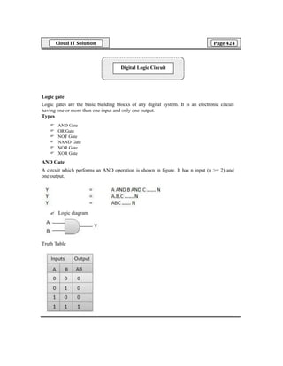
  • 1. Cloud IT Solution Page 424 Logic gate Logic gates are the basic building blocks of any digital system. It is an electronic circuit having one or more than one input and only one output. Types  AND Gate  OR Gate  NOT Gate  NAND Gate  NOR Gate  XOR Gate AND Gate A circuit which performs an AND operation is shown in figure. It has n input (n >= 2) and one output.  Logic diagram Truth Table Digital Logic Circuit
  • 2. Cloud IT Solution Page 425 OR Gate A circuit which performs an OR operation is shown in figure. It has n input (n >= 2) and one output. Logic diagram Truth Table NOT Gate NOT gate is also known as Inverter. It has one input A and one output Y.  Logic diagram
  • 3. Cloud IT Solution Page 426 Truth Table NAND Gate A NOT-AND operation is known as NAND operation. It has n input (n >= 2) and one output. Logic diagram Truth Table NOR Gate A NOT-OR operation is known as NOR operation. It has n input (n >= 2) and one output.
  • 4. Cloud IT Solution Page 427 Logic diagram Truth Table XOR Gate XOR or Ex-OR gate is a special type of gate. It can be used in the half adder, full adder and subtractor. The exclusive-OR gate is abbreviated as EX-OR gate or sometime as X-OR gate. It has n input (n >= 2) and one output. Logic diagram Truth Table
  • 5. Cloud IT Solution Page 428 XNOR Gate XNOR gate is a special type of gate. It can be used in the half adder, full adder and subtractor. The exclusive-NOR gate is abbreviated as EX-NOR gate or sometime as X-NOR gate. It has n input (n >= 2) and one output Logic diagram Truth Table NAND and NOR Universal Gate  NAND and NOR are called universal gates because all the other gates like and,or,not,xor and xnor can be derived from it.  Any basic gate can be implemented using NAND and NOR.
  • 6. Cloud IT Solution Page 429 De Morgan's Theorems  De Morgan has suggested two theorems which are extremely useful in Boolean Algebra. Theorem 1  The left hand side (LHS) of this theorem represents a NAND gate with inputs A and B, whereas the right hand side (RHS) of the theorem represents an OR gate with inverted inputs.
  • 7. Cloud IT Solution Page 430 This OR gate is called as Bubbled OR. Table showing verification of the De Morgan's first theorem – Theorem 2 The LHS of this theorem represents a NOR gate with inputs A and B, whereas the RHS represents an AND gate with inverted inputs.
  • 8. Cloud IT Solution Page 431 his AND gate is called as Bubbled AND. Table showing verification of the De Morgan's second theorem – Half Adder Half adder is a combinational logic circuit with two inputs and two outputs. The half adder circuit is designed to add two single bit binary number A and B. It is the basic building block for addition of two single bit numbers. This circuit has two outputs carry and sum.
  • 9. Cloud IT Solution Page 432 Truth Table Circuit Diagram Full Adder Full adder is developed to overcome the drawback of Half Adder circuit. It can add two one- bit numbers A and B, and carry c. The full adder is a three input and two output combinational circuit. Truth Table
  • 10. Cloud IT Solution Page 433 Circuit Diagram Full adder using two half adder K-map Karnaugh introduced a method for simplification of Boolean functions in an easy way. This method is known as Karnaugh map method or K-map method. It is a graphical method, which consists of 2n cells for ‘n’ variables. Variable K-Map
  • 11. Cloud IT Solution Page 434 Variable K-Map Variable K-Map Example Let us simplify the following Boolean function, f(W, X, Y, Z)= WX’Y’ + WY + W’YZ’ using K-map.
  • 12. Cloud IT Solution Page 435 Simplified Boolean function is: f= WX’ + WY + YZ’ Example Let us simplify the following Boolean function, f(X,Y,Z)=∏M(0,1,2,4) using K-map. Simplified Boolean function is: f=(X+Y).(Y+Z).(Z+X)
  • 13. Cloud IT Solution Page 436 Latch There are two types of memory elements based on the type of triggering that is suitable to operate it. 1. Latches 2. Flip-flops  Latches operate with enable signal, which is level sensitive. Whereas, flip-flops are edge sensitive. We will discuss about flip-flops in next chapter. Now, let us discuss about SR Latch & D Latch one by one.  SR latch example Flip-flops  A flip-flop or latch is a circuit that has two stable states and can be used to store state information. A flip-flop is a bistable multivibrator. The circuit can be made to change state by signals applied to one or more control inputs and will have one or two outputs. It is the basic storage element in sequential logic. Flip-flops and latches are fundamental building blocks of digital electronics systems used in computers, communications, and many other types of systems  There are mainly four types of flip flops that are used in electronic circuits. They are 1. The basic Flip Flop or S-R Flip Flop 2. Delay Flip Flop [D Flip Flop] 3. J-K Flip Flop 4. T Flip Flop S-R Flip Flop  The SET-RESET flip flop is not designed with the help of two NOR gates and also two NAND gates. These flip flops are also called S-R Latch.
  • 14. Cloud IT Solution Page 437 S-R Flip Flop using NOR Gate S-R Flip Flop using NAND Gate
  • 15. Cloud IT Solution Page 438 J-K Flip Flop Difference between CISC and RISC CISC RISC It is prominent on Hardware It is prominent on the software It has high cycles per second It has low cycles per second It has transistors used for storing Instructions which are complex More transistors are used for storing memory LOAD and STORE memory to memory is induced in instructions LOAD and STORE register to register are independent It has multi-clock It has single-clock
  • 16. Cloud IT Solution Page 439 1. The output of an AND gate with three inputs, A, B, and C, is HIGH when ________. A) A = 1, B = 1, C = 0 B)A = 0, B = 0, C = 0 C)A = 1, B = 1, C = 1 D)A = 1, B = 0, C = 1 2. If a 3-input NOR gate has eight input possibilities, how many of those possibilities will result in a HIGH output? A. 1 B. 2 C. 7 D. 8 3. If a signal passing through a gate is inhibited by sending a LOW into one of the inputs, and the output is HIGH, the gate is a(n): A. AND B. NAND C. NOR D. OR 4. A device used to display one or more digital signals so that they can be compared to expected timing diagrams for the signals is a: A. DMM B. spectrum analyzer C. logic analyzer D. frequency counter 5. When used with an IC, what does the term QUAD indicate? A. 2 circuits B. 4 circuits C. 6 circuits D. 8 circuits 6. The output of an OR gate with three inputs, A, B, and C, is LOW when ________. A) A = 0, B = 0, C = 0 B) A = 0, B = 0, C = 1 C) A = 0, B = 1, C = 1 D) all of the above 7. Which of the following logical operations is represented by the + sign in Boolean algebra? A. inversion B. AND C. OR D. complementation 8. Output will be a LOW for any case when one or more inputs are zero for a(n): A. OR gate B. NOT gate C. AND gate D. NOR gate 9. How many pins does the 4049 IC have? A. 14 B. 16 C. 18 D. 20 10. Which of the following choices meets the minimum requirement needed to create specialized waveforms that are used in digital control and sequencing circuits? A. basic gates, a clock oscillator, and a repetitive waveform generator B. basic gates, a clock oscillator, and a Johnson shift counter C. basic gates, a clock oscillator, and a DeMorgan pulse generator D. basic gates, a clock oscillator, a repetitive waveform generator, and a Johnson shift counter 1 2 3 4 5 6 7 8 9 10 C A B C B A C C B A Model Test Answer Model Test